Production Performance of the ATLAS Semiconductor Tracker Readout System
Abstract
The ATLAS Semiconductor Tracker (SCT) together with the pixel and the transition radiation detectors will form the tracking system of the ATLAS experiment at LHC. It will consist of 20 000 single-sided silicon microstrip sensors assembled back-to-back into modules mounted on four concentric barrels and two end-cap detectors formed by nine disks each. The SCT module production and testing has finished while the macro-assembly is well under way. After an overview of the layout and the operating environment of the SCT, a description of the readout electronics design and operation requirements will be given. The quality control procedure and the DAQ software for assuring the electrical functionality of hybrids and modules will be discussed. The focus will be on the electrical performance results obtained during the assembly and testing of the end-cap SCT modules.
Index Terms:
ATLAS, data acquisition, quality control, silicon radiation detectors.I Introduction
The ATLAS detector [1] is one of the two general-purpose experiments currently under construction for the Large Hadron Collider (LHC) at CERN. LHC is a proton-proton collider with a 14-TeV centre-of-mass energy and a design luminosity of . ATLAS consists of the Inner Detector (ID), the electromagnetic and the hadronic calorimeters, and the muon spectrometer. The ID [2] is a system designed for tracking, particle identification and vertex reconstruction, operating in a 2-T superconducting solenoid. The Semiconductor Tracker (SCT) forms the middle layer of the ID between the pixel detector and the transition radiation detector.
The SCT system [2, 3], depicted in Fig. 1, comprises a barrel made of four nested cylinders and two end-caps of nine disks each. The cylinders together carry 2112 detector units (modules) while 1976 end-cap modules are mounted on the disks in total. The whole SCT occupies a cylinder of 5.6 m in length and 56 cm in radius with the innermost layer at a radius of 27 cm. It provides a pseudorapidity coverage of up to .

The silicon modules [4] consist of one or two pairs of single-sided p-in-n microstrip sensors glued back-to-back at a 40-mrad stereo angle to provide two-dimensional track reconstruction. The 285- thick sensors [5] have 768 AC-coupled strips with an pitch for the barrel and a 57– pitch for the end-cap modules. Between the sensor pairs there is a highly thermally conductive baseboard. Barrel modules follow one common design, while for the forward ones four different types exist based on their position in the detector.
The readout of the module is based on 12 ABCD3TA ASICs manufactured in the radiation-hard DMILL process mounted on a copper/kapton hybrid [6]. The ABCD3TA chip [7] features a 128-channel analog front end consisting of amplifiers and comparators and a digital readout circuit operating at a frequency of 40.08 MHz. This ASIC utilizes the binary scheme where the signals from the silicon detector are amplified, compared to a threshold and only the result of the comparison enters the input register and the digital pipeline. The clock and command signals as well as the data are transferred from and to the off-detector electronics through optical links.
The ID volume will be subject to a fluence of charged and neutral particles from the collision point and from back-scattered neutrons from the calorimeters. An estimated fluence at the innermost part of the SCT is 1-MeV-neutrons (or equivalently 24-GeV-protons) in ten years of operation. The SCT has been designed to be able to withstand these fluences [8] and its performance has been extensively studied in beam tests using irradiated SCT modules [9].
II Electrical requirements
The LHC operating conditions demand challenging electrical performance specifications for the SCT modules and the limitations [10] mainly concern the accepted noise occupancy level, the tracking efficiency, the timing and the power consumption. The most important requirements the SCT module needs to fulfil follow.
II-1 Noise performance
The total effective noise of the modules results from two principal contributions; the front-end electronics and the channel-to-channel threshold matching. The former is the Equivalent Noise Charge ( ENC) for the front-end system including the silicon strip detector. It is specified to be less than 1500 ENC before irradiation and 1800 ENC after the full dose of 24-GeV-equivalent-protons. The noise hit rate needs to be significantly less than the real hit occupancy to ensure that it does not affect the data transmission rate, the pattern recognition and the track reconstruction. The foreseen limit of per strip requires the discrimination level in the front-end electronics to be set to 3.3 times the noise charge. To achieve this condition at the ATLAS operating threshold of 1 fC, the total equivalent noise charge should never be greater than 1900 ENC. Assuming a 3.3-fC median signal at full depletion that corresponds to a median signal-to-noise ratio of 10:1.
II-2 Tracking efficiency
In general the tracking performance of a particle detector depends on various parameters: the radial space available in the cavity, which limits the lever arm, the strength of the magnetic field, and the intrinsic precision and efficiency of the detector elements. To this respect a starting requirement is a low number of dead readout channels, specified to be less than 16 for each module to assure at least 99% of working channels. Furthermore no more than eight consecutive faulty channels are accepted in a module.
II-3 Timing requirements
For a correct track reconstruction, every hit has to be associated to a specific bunch crossing. That is translated to a demand for a time-walk of less than 16 ns, where the time-walk is defined as the maximum time variation in the crossing of the comparator threshold at 1 fC over a signal range of 1.25 to 10 fC. The fraction of output signals shifted to the wrong beam crossing is required to be less than 1%.
II-4 Power consumption
The nominal values for the power supplies of the ASICs are set as follows:
- •
Analogue power supply: .
- •
Digital power supply: .
- •
Detector-bias: high voltage of up to 500 V can be delivered by the ASICs.
The nominal power consumption of a fully loaded module is 4.75 W during operation at 1 fC threshold with nominal occupancy (1%) and 100 kHz trigger rate (L1 rate). Including the optical readout, the maximal power dissipation should be 7.0 W for the hybrid and the heat generated in the detectors just before thermal run-away should be 2.6 W for outer module wafers and 1.6 W for inner ones.
II-5 Double pulse resolution
The double pulse resolution directly affects the efficiency. It is required to be 50 ns to ensure less than 1% data loss at the highest design occupancy.
Standard DAQ system and electrical tests, described in the following sections, aim at verifying the hybrid and detector functionality after the module assembly and at demonstrating the module performance with respect to the required electrical specifications.
III Data acquisition system
In all the measurements performed, the ASICs are powered and read out electrically via the standard SCT DAQ system which contains the following VME modules:
- •
CLOAC (CLOck And Control): This module generates the clock, fast trigger and reset commands for the SCT modules in the absence of the timing, trigger and control system.
- •
SLOG (SLOw command Generator): It allows the generation of slow commands for the control and configuration of SCT front-end chips for up to six modules. It fans out clock and fast commands from an external source (CLOAC). Alternatively an internal clock may be selected, allowing SLOG to generate clock and commands in stand-alone mode.
- •
MuSTARD (Multichannel Semiconductor Tracker ABCD Readout Device): A unit designed to receive, store and decode the data from multiple SCT module systems. Up to 12 data streams (six modules) can be read out from one MuSTARD.
- •
SCTHV: A prototype high voltage unit providing detector bias to four modules.
- •
SCTLV: A custom-designed low voltage power supply for two silicon modules.
The software package SCTDAQ [11] has been developed for testing both the bare hybrids and the modules using the aforementioned VME units. It consists of a C++ dynamically linked library (STDLL) and a set of ROOT [12] macros which analyze the raw data obtained in each test and stores the results in a database [14]. A schematic diagram of the SCTDAQ is shown in Fig. 2.

IV Characterization tests

Every module is characterized to check the functionality and performance stability and to verify that the specifications are met. Using the internal calibration circuit to inject charge of adjustable amplitude in the preamplifier of each channel, the front-end parameters such as gain, noise and channel-to-channel threshold spread are measured. The characterization sequence [13] includes the following steps:
- •
Digital tests are executed to identify chip or hybrid damage. These include tests of the redundancy links, the chip by-pass functionality and the 128-cell pipeline circuit.
- •
Optimization of the delay between calibration signal and clock (strobe delay) is performed on a chip-to-chip basis.
- •
To minimize the impact of the threshold non-uniformity across the channels on the noise occupancy, the ABCD3TA design foresees the possibility to adjust the discriminator offset. A threshold correction using a digital-to-analog converter (Trim DAC) per channel with four selectable ranges (different for each chip) has been implemented in the ASICs. The trimming procedure allows an improved matching of the comparators thresholds; this is an important issue for the irradiated modules due to the increase of threshold spread with radiation dose.
- •
The gain and electronic noise are obtained channel by channel with threshold scans performed for ten different values of injected charge ranging from 0.5 to 8 fC (Response Curve procedure; see Fig. 4). For each charge injected the corresponding value in mV is extracted as the 50% point () of the threshold scan fitted with a complementary error function (-curve). The gain, input noise and offset are deduced from the correlation of the voltage output in mV versus the injected charge in fC.
- •
A threshold scan without any charge injection is performed to yield a direct measurement of the noise occupancy at 1 fC, as shown in Fig. 3. The adjusted discriminator offset is applied to ensure a uniform measurement across the channels.
- •
A dedicated scan is also executed to determine the time-walk. Setting the comparator threshold to 1 fC for each value of injected charge ranging from 1.25 to 10 fC a complementary error function is fitted to the falling edge of a plot of efficiency versus the setting of the strobe delay to determine the 50%-efficiency point. The time-walk is given by the difference between delays calculated for 1.25 fC and for 10 fC injected charge.

As part of the quality assurance test, a long-term test with electrical readout is also performed. The ASICs are powered, clocked and triggered during at least 18 hours while the module bias voltage is kept at 150 V and its thermistor temperature is . The bias voltage, chip currents, hybrid temperature, the leakage current and the noise occupancy are recorded every 15 min, as shown in Fig. 5. Moreover, every two hours a test verifying correct functionality of the module is performed.

A final measurement of the detector leakage current as a function of the bias voltage ( curve) is also performed at to assure that the current drawn by the whole module is low enough for the safe operation of the detector. The current values at 150 and 350 V are recorded and compared with those of previous curve measurements before and after the module sub-assembly.
During the electrical tests the modules are mounted in a light-tight aluminum box which supports the modules at the two cooling blocks of the baseboard. The test box includes a cooling channel connected to a liquid coolant system of adjustable temperature. The operating temperature is monitored by thermistors (one for the end-cap and two for the barrel hybrid) mounted on the hybrid. The box also provides a connector for dry air circulation. Subsequently, the module test box is placed inside an environmental chamber and it is electrically connected to the readout system and VME crate. Up to six modules can be tested simultaneously with this configuration. The grounding and shielding scheme of the setup is of crucial importance, therefore a careful optimization is necessary. The tests are carried out at a detector bias of 150 V and at an operating temperature of .
V Production modules performance
All production modules have to pass successfully the aforementioned tests —long-term test, characterization and leakage current measurement— as a part of their quality assurance plan. The hybrids are also tested before assembly using the same setup and software package. The results presented here correspond to the end-cap production modules that qualified for assembly onto disks, which amount to (including spares) representing about half of the total number of SCT modules.
In Fig. 6 the average gain per module is shown for all qualified forward modules. The average gain value is about 57 mV/fC at a discriminator threshold of 2 fC and it is of the same level as the one obtained from system tests.

The noise level per module is shown in Fig. 7. The two distinct contributions reflect the difference between short modules (inner and short middle) and long ones (long middle and outer). The former consist on only one pair of sensors having a strip length of around 6 cm, while the latter have two detector pairs with a total length of 12 cm, resulting in higher strip resistance.


An average of 1550 with an r.m.s. of about has been attained for the long modules. The noise occupancy at a comparator threshold of 1 fC is measured to be on average, i.e. twenty times lower than the requirement of per strip, as illustrated in Fig. 8. These values are compatible with the ones acquired from non-irradiated prototype modules [15], which also showed that after irradiation the noise levels although higher do not compromise the overall detector performance. It should be stressed that the acquired noise measurements largely depend on the degree of the setup optimization which generally varies across the testing sites, resulting in a higher than actual measured value of the module noise. The noise also depends on the temperature on the hybrid increasing by per degree Celsius. Since under standard conditions at the LHC the modules will operate with a thermistor temperature near , a lower noise level than the one obtained during quality control tests is expected during running.
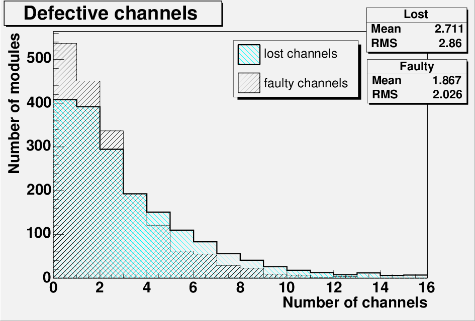
Another aspect of the readout requirements is the number of defective channels per module. As shown in Fig. 9, on average less than three channels per module are lost, i.e., have to be masked, which represents a fraction of . This category includes dead, stuck, noisy channels, as well as channels that have not been wire-bonded to the strips and channels that cannot be trimmed. Other channels exhibit less critical defects such as low or high gain (or offset) with respect to the chip-average. These faulty channels amount to less than two per module (). Their presence is due either to chip defects or defective detector strips (e.g. punch-through or short-circuited channels).
As far as the final curves are concerned, the full statistics results verify the good behavior of the sensors at a high bias voltage. The very few cases where a problem was observed was either due to detector damage after assembly or to a defective bias voltage connection on the hybrid. In the latter case the hybrids were reworked to re-establish the connection.
To recapitulate, only a fraction of about 2.4% of the tested modules does not pass at least one electrical characterization test. Most of these modules exhibit a high number of consecutive faulty channels due to minor damage (scratch) of module components such as the sensors or the fan-ins.11 1 The fan-ins are designed to provide electrical connection between the ABCD chips and the silicon strips and mechanical support between the hybrid and the sensors. They are made out of metal tracks deposited on top of a glass substrate. The high yield of the electrical tests performed on the production modules reflects the strict quality control criteria set during the ASICs and the hybrids selection.
VI Conclusion
The results of the systematic electrical tests performed in all SCT forward production modules demonstrate that they are well within specifications. The attained gain and the noise performance are compatible with the ones obtained in several system tests involving detector and electronics prototypes. The fraction of defective channels per module is kept well below 1%. The production of the silicon modules has finished and their mounting onto large structures (cylinders and disks) is well under way. The whole SCT is expected to be ready for installation in the ATLAS cavern at the LHC —together with the transition radiation detector— in spring 2006.
Acknowledgment
The author would like to thank Carlos Lacasta and Joe Foster for their help in retrieving the data presented here from the corresponding database and for useful comments during the preparation of this contribution.
References
- [1] ATLAS Collaboration, ATLAS Technical Proposal, CERN/LHCC/94-43 (1994); http://atlas.web.cern.ch/Atlas/
- [2] ATLAS Collaboration, Inner Detector Technical Design Report vol. I & II, CERN/LHCC/97-16 & CERN/LHCC/97-17 (1997).
- [3] For a recent review see: J. N. Jackson [ATLAS SCT Collaboration], Nucl. Instrum. Meth. A 541 (2005) 89.
- [4] C. Lacasta, Nucl. Instrum. Meth. A 512 (2003) 157.
- [5] D. Robinson et al., Nucl. Instrum. Meth. A 485 (2002) 84.
- [6] C. Ketterer, IEEE Trans. Nucl. Sci. 51 (2004) 1134.
- [7] W. Dabrowski, Nucl. Instrum. Meth. A 501 (2003) 167.
- [8]
I. Mandic [ATLAS SCT Collaboration],
IEEE Trans. Nucl. Sci. 49 (2002) 2888;
P. J. Dervan [ATLAS SCT Collaboration], Nucl. Instrum. Meth. A 514 (2003) 163;
P. K. Teng et al., Nucl. Instrum. Meth. A 497 (2003) 294;
L. S. Hou, P. K. Teng, M. L. Chu, S. C. Lee and D. S. Su, Nucl. Instrum. Meth. A 539 (2005) 105. - [9]
Y. Unno et al.,
IEEE Trans. Nucl. Sci. 49 (2002) 1868;
F. Campabadal et al., Nucl. Instrum. Meth. A 538 (2005) 384. - [10] C. Lacasta, “Electrical specifications and expected performance of the end-cap module,” ATLAS Project Document, ATL-IS-EN-0008 (2002), https://edms.cern.ch/document/316205/1
- [11] http://sct-testdaq.home.cern.ch/sct-testdaq/sctdaq/sctdaq.html
- [12] http://root.cern.ch
- [13] P. W. Phillips and L. Eklund, “Electrical tests of SCT hybrids and modules,” ATLAS internal document, http://hepwww.rl.ac.uk/atlas-sct/documents/Electrical_Tests.htm
- [14] C. Lacasta, F. Anghinolfi, J. Kaplon, R. Szczygiel, W. Dabrowski, P. Demierre and D. Ferrere, “Production database for the ATLAS-SCT front end ASICs,” Proc. 6th Workshop on Electronic for LHC Experiments, Cracow, Poland, 11-15 Sep 2000 [CERN-2000-010] (2000).
- [15]
C. Lacasta et al., “Electrical results from
prototype modules,” ATLAS Project Document, ATL-IS-TR-0001 (2002),
https://edms.cern.ch/document/316209/1;
P. W. Phillips [ATLAS SCT Collaboration], “System performance of ATLAS SCT detector modules,” Proc. 8th Workshop on Electronics for LHC Experiments, Colmar, France, 9-13 Sep 2002 [CERN-2002-003], p. 100–104 (2002).