physics/0604199
D0 Note CONF-5085 (2006)
Alignment of the Central DØ Detector** * Presented at the workshop on Tracking In high Multiplicity Environments, TIME’05, Zurich, October 3-7, 2005. Proceedings Nucl. Inst. Methods A.
André Sopczak
on behalf of the DØ Collaboration
Lancaster University
Abstract
1 Introduction
The alignment of the DØ tracking detectors is crucial for many physics analyses. The precision determination of the detector element positions improves the track reconstruction and the precision measurements at the interaction point. This is particularly important for Higgs, top and B-physics, and for an impact parameter trigger. A general overview of the DØ detector [1] and operation [2] has recently been given. Figure 1 shows the central DØ detector, Fig. 2 gives the positions of the barrel wafers and F-disk wedges, and Fig. 3 displays a side-view of the SMT with barrels, F-disks and H-disks.

2 Method and alignment procedure
The basic method to align the wafers is to minimize axial-residuals and z-residuals (Fig. 4). In the SMT, there are 432 barrel wafers, 144 F-disk wedges, and 96 H-disk wedges. The CFT encompasses 304 ribbons (each with 256 parallel scintillating fibers, 1.6 or 2.5 m long). In total 976 elements require alignment. The initial position of the sensitive barrel elements were determined from metrology measurements.
The alignment procedure is as follows: a track is fitted with all hits, except the hit from the sensitive element to be aligned. Then, axial-residuals and z-residuals of the hit on the wafer to be aligned, are determined. The pull (residual/error) is calculated and the corresponding as a sum of pulls from all tracks on the wafer are determined. The is minimized as a function of the wafer position (three space coordinates and three angles). All wafer positions are determined and these positions serve as input geometry for the next iterative step. The iterative process continues until a convergence criterion is reached. A wafer is considered aligned if the shift divided by its uncertainty of a sensitive element between two iterations is less than a certain value. This value is called the ‘shift limit’.


For the barrel, Fig. 5 shows a histogram of the number of hits per wafer for 50,000 events, and shows the shifts of each wafer between two consecutive iterations for the first and last iteration, illustrating the convergence. The corresponding plots for the F-disk and CFT are shown in Figs. 6 and 7. The number of tracks per event and the per degree of freedom for the track reconstruction show an improvement after alignment (Fig. 8). A shift limit of 0.07 is applied.


3 Residuals
For the barrel, the axial residuals before and after alignment are shown for all wafers, and for each individual wafer (Fig. 9). Figure 10 shows the corresponding plots for the F-disks. The residuals in the z-direction are given in Figs. 11 and 12.


4 Optimization of convergence
In order to improve the alignment process, the convergence speed, the accuracy and the dependence on the number of input events have been studied. Figure 13 shows the number of wafers to be aligned as a function of the iteration number for a shift limit of 0.05. For this shift limit value no convergence is obtained. The required numbers of iterations for convergence with larger shift limits is also shown.
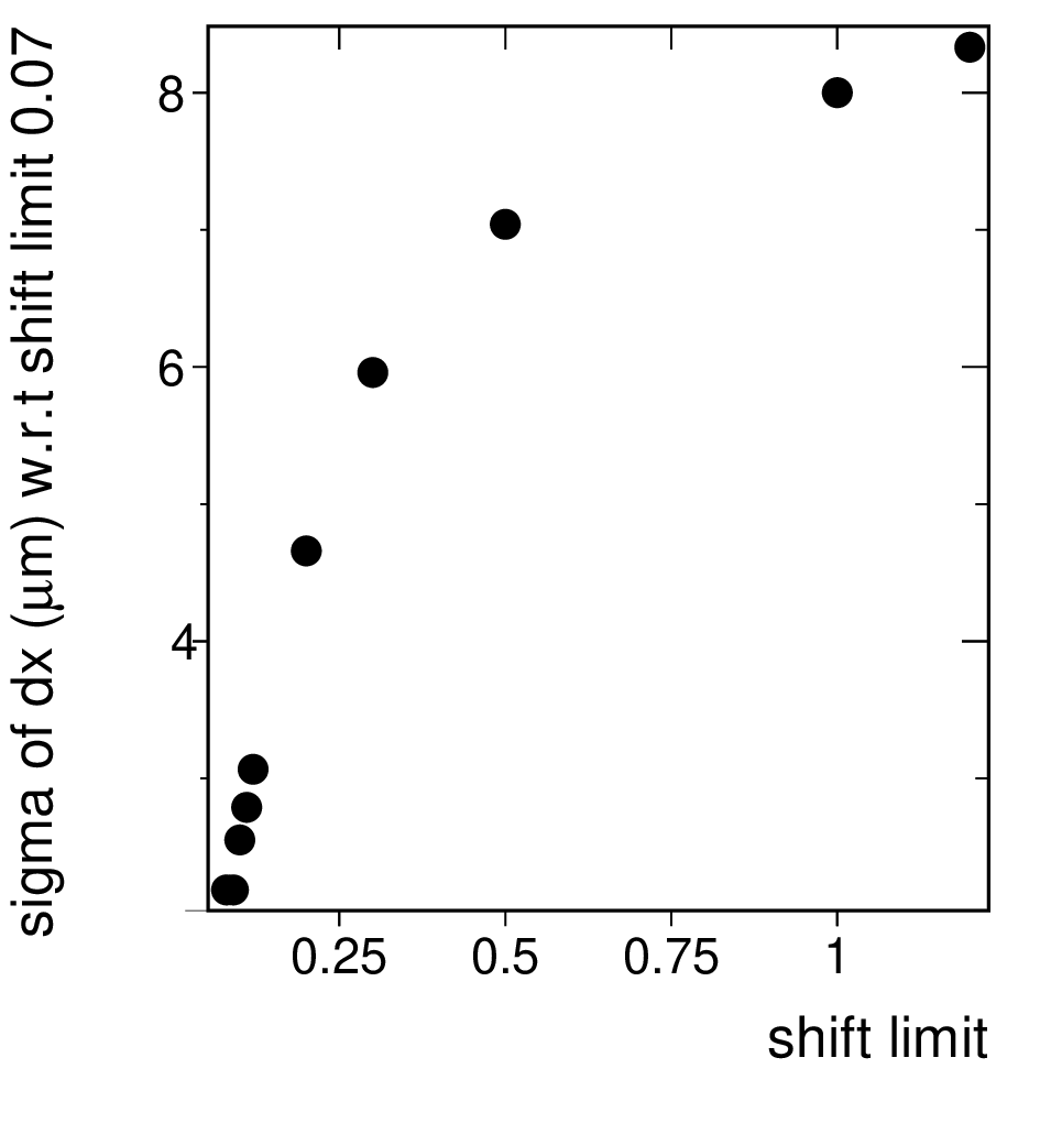
The variation between two aligned geometries for the same data and two different shift limits has been studied. The differences in x and y-directions between two barrel geometries for one geometry produced for shift limit 0.07, and the second one for 0.08 are shown in Figs. 14 and 15. The differences in x-direction between geometries produced with different shift limits are also shown in Fig. 14 as a function of the shift limit. For small shift limits the variation is below m. While a very good precision of the relative wafer positions is obtained, a larger shift of the entire SMT position is possible even for a small variation of the shift limit parameter. The example in Fig. 15 shows a relative shift in y-direction of the SMT wafers with m, a very similar value as in the x-direction. However, the entire SMT is shifted between the two geometries by about 9m. This corresponds to an oscillating behaviour of the axial shift as a function of the wafer id.




In addition, the dependence of the wafer positions on the number of input events has been studied (Fig. 16). Variations of the wafer positions in the aligned geometries below m are expected for more than 30,000 data input events. In a first step the shift limit has been reduced from 0.07 to 0.05, and in a further step it has been reduced from 0.05 to 0.04. Convergence was achieved by using the aligned 0.05 geometry as starting geometry for the 0.04 run. The convergence is illustrated in Fig. 17.


5 Uncertainties from procedure variations
In order to determine the uncertainty in the alignment procedure the CFT geometries are compared for two cases a) when SMT and CFT were aligned simultaneously, and b) when the SMT was aligned first, and then the CFT was aligned. No significant effect on the alignment was observed (Fig. 18).


6 Single wafer re-alignment precision
Furthermore, in order to test the re-alignability and the corresponding systematic uncertainty, one wafer was misaligned by 50m w.r.t. the original aligned geometry, and subsequently re-aligned. Remarkably, in the first iteration of the re-alignment 432 elements were shifted. After re-alignment all elements were within m of the original position. The geometries before and after re-alignment are compared to the original geometry (Fig. 19).

7 Longevity / variation of active elements
Figure 20 shows the variation of the number of disabled elements with time. During each data-taking shutdown several disabled elements were repaired.

8 Single wafer alignment in data rerun
After data-taking shutdowns some additional wafers become operational and require alignment. Figure 21 shows an example of residuals for a single wafer (mean value of the fitted Gaussian) before and after alignment.
| high | low | |
|---|---|---|
| 16.0 | 13.3 | |
| 3.6 | 0.1 |

9 Alignability of wafers from different runs
As some wafers are non-operational depending on the time period of data-taking, the combination of data from different time periods improves the overall alignment. Table 1 summarizes the numbers of aligned wafers for different data-taking periods.
| Period | dates | alignable wafers |
|---|---|---|
| B1 | Oct. 24, 2002 | 827 |
| B2 | Oct. 24, 2002 | 827 |
| A | April 20, 2003 | 813 |
| C | Aug. 10, 2003 | 794 |
| A+B1+B2+C | mixed | 843 |
10 Time stability of detector alignment
The detector alignment has been performed for different time periods. In order to determine the alignment precision two aligned geometries from different time periods are compared. An example is given in Fig. 22 for period 1 and 5. The time stability of the detector for various time periods between April 2002 and December 2004 has been studied and no significant variation is observed (Fig. 23).
| Period | dates |
|---|---|
| 1 (B1,B2) | Oct. 24, 2002 |
| 2 (A) | April 20, 2003 |
| 3 (C) | Aug. 10, 2003 |
| 4 (D) | Jan. 18, 2004 |
| 5 (E) | Aug. 17, 2004 |
| 6 (F) | Dec. 18, 2004 |


11 Local alignment: metrology
In addition to the previously described global alignment, where wafers are considered ideal planes with no structure, the local alignment has been investigated. Local alignment refers to the alignment on a given sensitive element. As an example, the wafer geometry and the separation in z-direction is shown in Fig. 25. Figure 24 illustrates the positions of the fiducial points on the wafers. This is particulary interesting as some wafers are made of two independent silicon plates. The precision in the distance of two fiducial points for detector elements made of the two sensors is given in Fig. 26 from metrology. No indication of a shift in the survey between these plates is observed and variations are within m.


12 Influence on physics results
In order to determine the resolution of the Distance of Closest Approach, DCA, the position of the beamspot has been determined. A displaced beamspot position in the r- plane corresponds to a sine dependance of the DCA as a function of the track direction . It is parametrized like and this function is fitted to the data as shown in Fig. 27. The figure shows also the DCA resolution. The DCA resolution depends on the transverse momentum of the track and Table 2 gives the DCA resolutions for different ranges. The DCA resolution consists of the beam-spot size convoluted with the Impact Parameter (IP) resolution. The beam-spot size is approximately 30-40m and depends on the machine optics.
The impact parameter resolution is crucial for the Silicon Track Trigger (STT). The beamspot determination of the previous run is used. The resulting impact parameter resolution is shown in Fig. 28.
| (GeV) | 0.2-0.5 | 0.5-1 | 1-3 | 3-5 | 5-10 | 10-20 | 20-50 |
|---|---|---|---|---|---|---|---|
| DCA res. (m) | 203 | 118 | 77 | 60 | 55 | 53 | 50 |
The impact parameter measurement is also an important aspect for b-quark tagging. Its resolution after alignment in the offline analysis together with the Monte Carlo prediction is shown in Fig. 29. Multiple scattering is the dominant source of resolution degradation at small values. The figure shows also the b-quark tagging efficiency versus the light quark mistag rate.
The alignment uncertainty contributes to the systematic errors in several physics analyses. The effect of the alignment uncertainty has been studied, for example, by assuming a constant shift of 10m in radial direction outward (Fig. 30) in order to estimate the impact on B-meson lifetime measurements. Only a small contribution to the systematic uncertainty from alignment in B-meson lifetime measurements is observed (Table 3).


| (m) | |
|---|---|
| Alignment | 2 |
| vertex | 3 |
| Model for resolution | 3 |
| Background | 4 |
| Total | 6 |
As examples of physics analyses where the detector alignment is crucial, results from lifetime measurements are shown in Figs. 31 and 32. The signal (shaded region) is clearly visible over the background (dotted line).


13 Conclusions and outlook
About 850 sensitive elements have been aligned. The alignment precision is close to design value (e.g. residuals: data m, simulation m). Some alignment parameters have been optimized. Systematic uncertainties of the alignment procedure are less than about m. The monitoring of the detector stability showed no significant movement. The alignment ensures excellent on-line and off-line b-tagging, and lifetime measurements, and is therefore crucial for Higgs, top, and B-physics. In spring 2006, a new inner layer [3], Layer-0, at 1.6 cm from the interaction point will be installed inside the current vertex detector, which will significantly improve the impact parameter resolution, as illustrated in Fig. 33.

References
- [1] DØ Collaboration, physics/0507191, submitted to Nucl. Inst. Methods A, “The Upgraded DØ Detector”.
- [2] R. Lipton, “DØ Tracking – From the Inside Looking Out”, these proceedings.
- [3] M. Weber, “A New Inner Layer Silicon Strip Detector for DØ”, these proceedings.
Acknowledgements
I would like to thank the organizers of the TIME’05 conference for their kind hospitality, and Tim Brodbeck, Aran Garcia-Bellido, Mike Hildreth, Alex Melnitchouk, Ulrich Straumann, Mike Strauss and Rick van Kooten for comments on the manuscript. Contributions from Guennadi Borrisov and Brian Davies are particularly acknowledged.