The Measurement of AM noise of Oscillators
![[Uncaptioned image]](0512082v1/logo-femto-st.png) Affiliation: [0.5em]
FEMTO-ST Institute
Affiliation: [-0.5ex]
CNRS and Université de Franche Comté,
Besançon, France
Affiliation: [1.5em]
Affiliation: [0.5em]
FEMTO-ST Institute
Affiliation: [-0.5ex]
CNRS and Université de Franche Comté,
Besançon, France
Affiliation: [1.5em]
Abstract
The close-in AM noise is often neglected, under the assumption that it is a minor problem as compared to phase noise. With the progress of technology and of experimental science, this assumption is no longer true. Yet, information in the literature is scarce or absent.
This report describes the measurement of the AM noise of rf/microwave sources in terms of , i.e., the power spectrum density of the fractional amplitude fluctuation . The proposed schemes make use of commercial power detectors based on Schottky and tunnel diodes, in single-channel and correlation configuration.
There follow the analysis of the front-end amplifier at the detector output, the analysis of the methods for the measurement of the power-detector noise, and a digression about the calibration procedures.
The measurement methods are extended to the relative intensity noise (RIN) of optical beams, and to the AM noise of the rf/microwave modulation in photonic systems.
Some rf/microwave synthesizers and oscillators have been measured, using correlation and moderate averaging. As an example, the flicker noise of a low-noise quartz oscillator (Wenzel 501-04623E) is , which is equivalent to an Allan deviation of . The measurement systems described exhibit the world-record lowest background noise.
| Symbol list | |
| , as in | average, or dc component [of the signal ] |
| , as in | ac component [of the signal ] |
| system bandwidth | |
| statistical expectation | |
| Fourier frequency (near dc) | |
| voltage gain (thus, the power gain is ) | |
| J/Hz, Planck constant | |
| coefficient of the power-law representation of noise, | |
| , | current, dc current |
| , | optical intensity (Sections 9–10) |
| J/K, Boltzmann constant | |
| detector gain, V/W. Also , , | |
| in cross-spectrum measurements, no. of averaged spectra | |
| modulation index (Sections 9–10) | |
| , | carrier power. Also , , , etc. |
| C, electron charge | |
| resistance | |
| characteristic resistance. Often | |
| rms | root mean square value |
| , | single-sided power spectrum density (of the quantity ) |
| time | |
| , | absolute temperature, reference temperature ( K) |
| (voltage) signal, as a funtion of time | |
| peak carrier voltage (not accounting for noise) | |
| thermal voltage. mV at 25 | |
| fractional amplitude fluctuation | |
| , as in | random fluctuation (of the quantity ) |
| , as in | deterministic fluctuation (of the quantity ) |
| diode technical parameter [Eq .(15)], | |
| photodetector quantum efficiency (Sections 9–10) | |
| wavelength | |
| , as in | in a subscript, means ‘light’ (as opposed to ‘microwave’) |
| , as in | in a subscript, means ‘microwave’ (as opposed to ‘light’) |
| , | frequency, carrier frequency |
| photodetector responsivity, A/W (Sections 9–10) | |
| Allan deviation of the quantity | |
| , as in | measurement time |
| phase fluctuation | |
1 Basics
A quasi-perfect rf/microwave sinusoidal signal can be written as
| (1) |
where is the fractional amplitude fluctuation, and is the phase fluctuation. Equation (1) defines and . In low noise conditions, that is, and , Eq. (1) is equivalent to
| (2) | |||
We make the following assumptions about , in agreement with actual cases of interest:
- 1.
The expectation of the amplitude is . Thus .
- 2.
The expectation of the frequency is . Thus .
- 3.
Low noise. and .
- 4.
Narrow band. The bandwidth of and is and .
It is often convenient to describe the close-in noise in terms of the single-side11 1 Most experimentalists prefer the single-side power spectrum density because all instruments work in this way. This is because the power can be calculated as , which is far more straightforward than integrating over positive and (to some extent, misterious) negative frequencies. power spectrum density , as a function of the Fourier frequency . A model that has been found useful to describe is the power-law . In the case of amplitiude noise, generally the spectrum contains only the white noise , the flicker noise , and the random walk . Accordingly,
| (3) |
Random walk and higher-slope phenomena, like drift, are often induced by the environment. It is up to the experimentalist to judge the effect of environment.
The spectrum density can be converted into Allan variance using the formulae of Table 2.
| noise type | Spectrum density | Allan variance |
|---|---|---|
| white | ||
| flicker | ||
| random walk |
The signal power is
| (4) | ||||
| thus | ||||
| (5) | ||||
It is convenient to rewrite as , with
| (6) |
The amplitude fluctuations are measured through the measurement of the power fluctuation ,
| (7) |
and of its power spectrum density,
| (8) |
The measurement of a two-port device, like an amplifier, is made easy by the availability of the reference signal sent to the device input. In this case, the bridge (interferometric) method [RG02] enables the measurement of amplitude noise and phase noise with outstanding sensitivity. Yet, the bridge method can not be exploited for the measurement of the AM noise of oscillators, synthesizers and other signal sources. Other methods are needed, based on power detectors and on suitable signal processing techniques.
2 Single channel measurement


Figure 1 shows the basic scheme for the measurement of AM noise. The detector characteristics (Sec. 4) is , hence the ac component of the detected signal is . The detected voltage is related to by , that is,
| (9) |
Turning voltages into spectra, the above becomes
| (10) |
Therefore, the spectrum of can be measured using
| (11) |
Due to linearity of the network that precedes the detector (directional couplers, cables, etc.), the fractional power fluctuation is the same in all the circuit, thus is the same. As a consequence, the separate measurement of the oscillator power and of the attenuation from the oscillator to the detector is not necessary. The straightforward way to use Eq. (10), or (11), is to refer at detector input, and at the detector output.
Interestingly, phase noise has virtually no effect on the measurement. This happens because the bandwidth of the detector is much larger than the maximum frequency of the Fourier analysis, hence no memory effect takes place.
In single-channel measurements, the background noise can only be assessed by measuring a low-noise source22 2 The reader familiar with phase noise measurements is used to measure the instrument noise by removing the device under test. This is not possible in the case of the AM noise of the oscillator.. Of course, this measurement gives the total noise of the source and of the instrument, which can not be divided. The additional hypothesis is therefore required, that the amplitude noise of the source is lower than the instrument background. Unfortunately, a trusted source will be hardly available in practice.
Calibration is needed, which consists of the measurement of the product . See Section 11.
3 Dual channel (correlation) measurement


Figure 2 shows the scheme for the correlation measurement of AM noise. The signal is split into two branches, and measured by two separate power detectors and amplifiers. Under the assumption that the two channels are independent, the cross spectrum is proportional to . In fact, the two dc signals are and . The cross spectrum is
| (12) |
from which
| (13) |
Averaging over spectra, the noise of the individual channels is rejected by a factor (Fig. 3), for the sensitivity can be significantly increased. A further advantage of the correlation method is that the measurement of is validated by the simultaneous measurement of the instrument noise limit, that is, the single-channel noise divided by . This solves one of the major problems of the single-channel measurement, i.e., the need of a trusted low-noise source.
Larger is the power delivered by the source under test, larger is the instrument gain. This applies to single-channel measurements, where the gain is [Eq. (10)], and to correlation measurements, where the gain is [Eq. (12)]. Yet in a correlation system the total power is split into the two channels, for . Hence, switching from single-channel to correlation the gain drops by a factor ( dB). Let us now compare a correlation system to a single-channel system under the simplified hypothesis that the background noise referred at the detector output is unchanged. This happens if the noise of the dc preamplifier is dominant. In such cases, the background noise referred to the instrument input, thus to , is multiplied by a factor . The numerator “4” arises from the reduced gain, while the denominator is due to averaging. Accordingly, it must be for the correlation scheme to be advantageous in terms of sensitivity. On the other hand, if the power of the source under test is large enough for the system to work at full gain in both cases, the dual-channel system exhibits higher sensitivity even at .
Calibration is about the same as for the single-channel measurements. See Section 11.
In laboratory practice, the availability of a dual-channel FFT analyzer is the most frequent critical point. If this instrument is available, the experimentalist will prefer the correlation scheme in virtually all cases.
4 Schottky and tunnel diode power detectors
A rf/microwave power detector uses the nonlinear response of a diode to turn the input power into a dc voltage . The transfer function is
| (14) |
which defines the detector gain . The physical dimension of is . The technical unit often used in data sheets is mV/mW, equivalent to . The diodes can only work at low input level. Beyond a threshold power, the output voltage differs smoothly from Eq. (14). The actual response depends on the diode type.

Figure 4 shows the scheme of actual power detectors. The input resistor matches the high input impedance of the diode network to the standard value over the bandwidth and over the power range. The value depends on the specific detector. The output capacitor filters the video33 3 From the early time of electronics, the term ‘video’ is used (as opposed to ‘audio’) to emphasize the large bandwidth of the demodulated signal, regardless of the real purposes. signal, eliminating carrier from the output. A low capacitance makes the detector fast. On the other hand, a higher capacitance is needed if the detector is used to demodulate a low-frequency carrier. The two-diode configuration provides larger output voltage and some temperature compensation.
| manufacturer | web site |
|---|---|
| Aeroflex/Metelics | aeroflex-metelics.com |
| Agilent Technologies | agilent.com |
| Advanced Control Components | advanced-control.com |
| Advanced Microwave | advancedmicrowaveinc.com |
| Eclipse | eclipsemicrowave.com |
| Herotek | herotek.com |
| Microphase | microphase.com/military/detectors.shtml |
| Omniyig | omniyig.com |
| RLC Electronics | rlcelectronics.com/detectors.htm |
| S-Team | s-team.sk |
Power detectors are available off-the-shelf from numerous manufacturers, some of which are listed on Table 3. Agilent Technologies provides a series of useful application notes [Agi03] about the measurement of rf/microwave power.
Two types of diode are used in practice, Schottky and tunnel. Their typical characteristics are shown in Table 4.
| Schottky | tunnel | |
| input bandwidth | up to 4 decades | 1–3 octaves |
| 10 MHz to 20 GHz | up to 40 GHz | |
| vsvr max. | 1.5:1 | 3.5:1 |
| max. input power (spec.) | dBm | dBm |
| absolute max. input power | 20 dBm or more | 20 dBm |
| output resistance | 1–10 k | 50–200 |
| output capacitance | 20–200 pF | 10–50 pF |
| gain | 300 V/W | 1000 V/W |
| cryogenic temperature | no | yes |
Schottky detectors are the most common ones. The relatively high output resistance and capacitance makes the detector suitable to low-frequency carriers, starting from some 10 MHz (typical). In this condition the current flowing through the diode is small, and the input matching to is provided by a low value resistor. Thus, the VSWR is close to 1:1 in a wide frequency range. Most of the input power is dissipated in the input resistance, which reduces the risk of damage in case of overload. A strong preference for negative output voltage seems to derive from the lower noise of P type Schottky diodes, as compared to N type ones, in conjunction with practical issues of mechanical layout. Figure 5 shows the response of a two-diode Schottky power detector. The quadratic response [Eq. (14)] derives from the diode resistance , which is related to the saturation current by
| (15) |
where is a parameter that derives from the junction technology; mV at room temperature is the thermal voltage. At higher input level, becomes too small and the detector response turns smoothly from quadratic to linear, like the response of the common AM demodulators and power rectifiers.


| detector gain, | ||
| load resistance, | DZR124AA | DT8012 |
| (Schottky) | (tunnel) | |
| 35 | 292 | |
| 98 | 505 | |
| 217 | 652 | |
| 374 | 724 | |
| 494 | 750 | |
| conditions: power to dBm | ||
Tunnel detectors are actually backward detectors. The backward diode is a tunnel diode in which the negative resistance in the forward-bias region is made negligible by appropriate doping, and used in the reverse-bias region. Most of the work on such detectors dates back to the sixties [Bur63, Gab67, Hal60]. Tunnel detectors exhibit fast switching and higher gain than the Schottky counterpart. A low output resistance is necessary, which affects the input impedance. Input impedance matching is therefore poor. In the measurement of AM noise, as in other applications in which fast response is not relevant, the output resistance can be higher than the recommended value, and limited only by noise considerations. At higher output resistance the gain further increases. Tunnel diodes also work in cryogenic environment, provided the package tolerates the mechanical stress of the thermal contraction.
Figures 6–7 and Table 5 show the conversion gain of two detectors, measured at the FEMTO-ST Institute. As expected, the Schottky detector leaves smoothly the quadratic law (true power detection) at some dBm, where it becomes a peak voltage detector. The response of the tunnel detector is quadratic up to a maximum power lower than that of the Schottky diode. This is due to the lower threshold of the tunnel effect. The output voltage shows a maximum at some 0 dBm, then decreases. This is ascribed to the tunnel-diode conduction in the forward region.
At the FEMTO-ST Institute, I routinely use the Herotek DZR124AA (Schottky) and DT8012 (tunnel). At the JPL, I have sometimes used the pair HP432A, and more recently the same Herotek types that I use at the LPMO. The old HP432A pair available shows an asymmetry of almost 10 dB in flickering, which causes experimental difficulties. This asymmetry might be a defect of the specific sample.
5 The double balanced mixer


Some articles from the NIST [NNW94]44 4 Fred Walls published some articles in the FCS Proceedings. Craig Nelson showed the method in his tutorial given at the 2003 FCS. suggest the use of a double balanced mixer as the power detector in AM noise measurements, with a configuration similar to that of Fig. 8. Higher sensitivity is obtained with cross-spectrum measurements, using two mixers. The double balanced mixer is operated in the following conditions:
- 1.
Both RF and LO inputs are not saturated.
- 2.
The RF and LO signals are in-phase.
At low frequencies the in-phase condition may be hard wired, omitting the variable phase shifter.
However useful, the available articles do not explain the diode operation in terms of electrical parameters. One can expect that the background noise of the mixer used as the AM detector can not be lower than that of a Schottky-diode power detector for the simple reason that the mixer contains a ring of Schottky diodes. One could guess that the use of the mixer for AM noise measurements originates from having had mixers and phase shifter on hand for a long time at the NIST department of phase noise.
6 Power detector noise
Two fundamental types of noise are present in a power detector, shot noise and thermal noise [Gab67, Sec. V]. In addition, detectors show flicker noise. The latter is not explained theoretically, for the detector characterization relies on experimental parameters. Some useful pieces of information are available in [Eng61].
Owing to the shot effect, the average current flowing in the diode junction is affected by a fluctuation of power spectral density
| (16) |
Using the Ohm law across the load resistor , the noise voltage at the detector output is
| (17) |
Then, the shot noise is referred to the input-power noise using . Thus, at the operating power it holds that
| (18) |
The thermal noise across load resistance has the power spectral density
| (19) |
which turns into
| (20) |
referred to the detector input. An additional thermal-noise contribution comes from the dissipative resistance of the diodes. This can be accounted for by increasing the value of in Equations (19) and (20). It should be remarked that diode differential resistance is not a dissipative phenomenon, for there is no thermal noise associated to it.

Figure 9 shows the equivalent input noise as a function of power. The shot noise is equal to the thermal noise, , at the critical power
| (21) |
It turns out that the power detector is always used in the low power region (), where shot noise is negligible. In fact, taking the data of Table 5 as typical of actual detectors, spans from dBm to dBm for the Schottky diodes (), and from dBm to dBm for the tunnel diodes (), depending on the load resistance. On the other hand, the detector turns from the quadratic (power) response to the linear (voltage) response at a significantly lower power. This can be seen on Figure 6 and 7.
Looking at the specifications of commercial power detectors, information about noise is scarce. Some manufacturers give the NEP (Noise Equivalent Power) parameter, i.e., the power at the detector input that produces a video output equal to that of the device noise. In no case is said whether the NEP increases or not in the presence of a strong input signal, which is related to precision. Even worse, no data about flickering is found in the literature or in the data sheets. Only one manufacturer (Herotek) claims the low flicker feature of its tunnel diodes, yet without providing any data.
The power detector is always connected to some kind of amplifier, which is noisy. Denoting with and the white and flicker noise coefficients of the amplifier, the spectrum density referred at the input is
| (22) |
The amplifier noise coefficient is connected to the noise figure by . Yet we prefer not to use the noise figure because in general the amplifier noise results from voltage noise and current noise, which depends on . Equation (22) is rewritten in terms of amplitude noise using [Eq. (7)]. Thus,
| (23) |
After the first term of Eq. (22), the critical power becomes
| (24) |
This reinforces the conclusion that in actual conditions the shot noise is negligible.
7 Design of the front-end amplifier
For optimum design, one should account for the detector noise and for the noise of the amplifier, and find the most appropriate amplifier and operating conditions. Yet, the optimum design relies upon the detailed knowledge of the power-detector noise, which is one of our targets (Sec. 8). Thus, we provisionally neglect the excess noise of the power detector. The first design is based on the available data, i.e., thermal noise and the noise of the amplifier. Operational amplifiers or other types of impedance-mismatched amplifiers are often used in practice. As a consequence, a single parameter, i.e., the noise figure or the noise temperature, is not sufficient to describe the amplifier noise. Voltage and current fluctuations must be treated separately, according to the popular Rothe-Dahlke model [RD56] (Fig. 10). The amplifier noise contains white and flicker, thus
| (25) | ||||
| (26) |
The design can be corrected afterwards, accounting for the flicker noise of the detector.

Single-channel systems
Accounting for shot and thermal noise, and for the noise of the amplifier, the noise spectrum density is
| (27) |
at the amplifier input, and
| (28) |
referred to the rf input. The detector gain depends on , thus the residual can not be arbitrarily reduced by decreasing . Instead, there is an optimum at which the system noise is at its minimum.
Correlation-and-averaging systems

The noise contribution of the amplifier can be reduced by measuring the cross spectrum at the output of two amplifiers connected to the power detector, provided that the noise of the amplifiers is independent. For this to be true, the optimum design of the front-end amplifier changes radically. Figure 11 points out the problem. The current noise of each amplifier turns into a random voltage fluctuation across the load resistance . Focusing only on the amplifier noise, the voltage at the two outputs is
The terms and are independent, for their contribution to the cross spectrum density is reduced by a factor , where is the number of averaged spectra. Conversely, a term
is present at the two outputs. This term is exactly the same, thus it can not be reduced by correlation and averaging. Consequently, the lowest current noise is the most important parameter, even if this is obtained at expense of a larger voltage noise. Yet, the rejection of larger voltage noise requires large , for some tradeoff may be necessary.
Examples
This section shows some design attempts, aimed at the lowest white and flicker noise at low Fourier frequencies, up to 0.1–1 MHz, where operational amplifiers can be exploited in a simple way.
A preliminary analysis reveals that, at the low resistance values required by the detector, BJT amplifiers perform lower noise than field-effect transistors. On the other hand, the noise rejection by correlation and average requires low current noise, for JFET amplifiers are the best choice. In fact, BJTs can not be used because of the current noise, while MOSFETs show noise significantly larger (10 dB or more) than JFETs.
| voltage | current | ||||
| type | white | flicker | white | flicker | notes |
| AD743 | 2.9 | 18 | 6.9 | jfet op-amp | |
| LT1028 | 0.9 | 1.7 | 1000 | 16 | bjt op-amp |
| MAT02 | 0.9 | 1.6 | 900 | 1.6 | npn bjt matched pair |
| MAT03 | 0.7 | 1.2 | 1200 | 11 | pnp bjt matched pair |
| OP27 | 3.0 | 4.3 | 400 | 4.7 | bjt op-amp |
| OP177 | 10 | 8.0 | 125 | 1.6 | bjt op-amp |
| OP1177 | 8.0 | 8.3 | 200 | 1.5 | bjt op-amp |
| OPA627 | 4.5 | 45 | 2.5 | jfet op-amp | |
| unit | |||||
Using two detectors (DZR124AA and DT8012), we try the operational amplifiers and transistor pairs listed on Table 6. These amplifiers are selected with the criterion that each one is a low-noise choice in its category.
- AD743 and OPA627
-
are general-purpose precision JFET amplifiers, which exhibit low bias current, hence low current noise. They are intended for correlation-and-averaging schemes (Fig. 11). The OP625 is similar to the OP627 but for the frequency compensation, which enables unity-gain operations, yet at expenses of speed. It is used successfully in the measurement of the excess noised of semiconductors, where large averaging size is necessary in order to rid of the amplifier noise [SFF99].
- LT1028
-
is a fast BJT amplifier with high bias current in the differential input stage. This feature makes it suitable to low-noise applications in which the source resistance is low. In fact, the optimum noise resistance is of 900 for white noise, and of 105 for flicker. These values are in the preferred range for proper operation of the power detectors.
- MAT02 and MAT03
-
are bipolar matched pairs. They exhibit lower noise than operational amplifiers, and they are suitable to the design for low resistance of the source, like the LT1028. The MAT03 was successfully employed in the design of a low-noise amplifier optimized for 50 sources [RLV04].
- OP27 and OP37
-
are popular general-purpose precision BJT amplifiers, most often used in low-noise applications. Their noise characteristics are about identical. The OP27 is fully compensated, for it is stable at closed-loop gain of one. The OP37 is only partially compensated, which requires a minimum closed-loop gain of five for stable operation. Of course, lower compensation increases bandwidth and speed.
- OP177 and OP1177
-
are general-purpose precision BJT amplifiers with low bias current in the differential input stage, thus they exhibit lower current noise than other BJT amplifiers. They can be an alternative if the design based on JFET amplifier fails.
In the try-and-error process, we take into account shot noise, thermal noise, amplifier voltage noise, and amplifier current noise. The total white noise is the sum of all them
| (29) | ||||||
| The total flicker accounts for the voltage and current of the amplifier | ||||||
| (30) | ||||||
| The correlated noise spectrum is equal to the total noise minus the voltage noise spectrum of the amplifier, which is independent | ||||||
| (31) | ||||||
| (32) | ||||||
The flicker noise of the detector, still not available, is to be added to Equations (30) and (32).


white noise
flicker noise
correlated white noise
correlated flicker noise ( only)
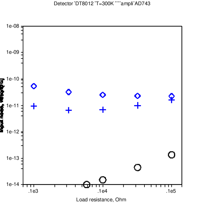


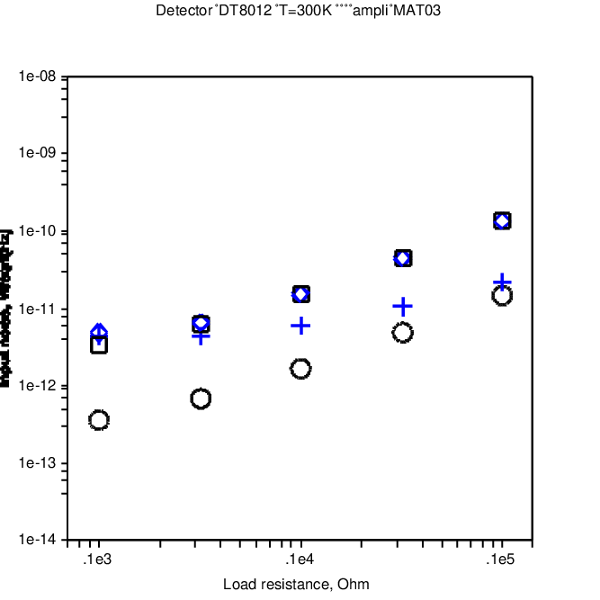


white noise
flicker noise
correlated white noise
correlated flicker noise ( only)
After evaluation, we discard the OP177 because the OP1177 exhibits superior performances in all noise parameters. Similarly, we discard the OP627 in favour of the AD743. The lower current noise of the OP627 can be exploited only at very large number of averages, which is impractical. On the other hand, the lower voltage noise of the AD743 helps to keep the number of averages reasonable. Figures 12 and 13 show a summary of the expected noise as a function of the load resistance . The symbols , , , have the same meaning in Equations (29)–(32) and in Figures 12 and 13. Analyzing the noise plots we restrict our attention to the detector-amplifier pairs of Table 7, in which we identify the following interesting configurations.
| Equivalent input noise | |||||||
|---|---|---|---|---|---|---|---|
| detector and amplifier | noise type | load resistance | unit | ||||
| 100 | 320 | 1000 | 3200 | 10000 | |||
| DZR124AA and AD743 | white | 99.2 | 39.5 | 22.8 | 19.6 | 24.5 | |
| flicker | 541 | 186 | 80.8 | 44.8 | 33.3 | ||
| correl. white | 0.050 | 0.042 | 0.052 | 0.089 | 0.205 | ||
| correl. flicker | – | – | – | – | – | ||
| DZR124AA and MAT02 | white | 54.7 | 27.5 | 19.6 | 19.8 | 29.2 | |
| flicker | 48.6 | 17.7 | 10.4 | 13.5 | 29.9 | ||
| correl. white | 4.06 | 3.45 | 4.24 | 7.28 | 16.7 | ||
| correl. flicker | 7.22 | 6.13 | 7.54 | 12.9 | 29.8 | ||
| DZR124AA and OP27 | white | 102 | 40.3 | 23.1 | 20.0 | 25.6 | |
| flicker | 131 | 48.0 | 29.4 | 39.5 | 87.8 | ||
| correl. white | 1.80 | 1.53 | 1.88 | 3.23 | 7.44 | ||
| correl. flicker | 21.2 | 18.0 | 22.1 | 38.0 | 87.4 | ||
| DT8012 and AD743 | white | 9.86 | 6.77 | 7.00 | 10.0 | 16.2 | |
| flicker | 53.7 | 32.0 | 24.8 | 22.8 | 22.1 | ||
| correl. white | 0.005 | 0.007 | 0.016 | 0.045 | 0.135 | ||
| correl. flicker | – | – | – | – | – | ||
| DT8012 and LT1028 | white | 5.44 | 4.72 | 6.06 | 10.2 | 20.1 | |
| flicker | 8.78 | 10.9 | 23.3 | 66.0 | 197 | ||
| correl. white | 0.448 | 0.657 | 1.45 | 4.12 | 12.3 | ||
| correl. flicker | 7.17 | 10.5 | 23.2 | 66.0 | 197 | ||
| DT8012 and MAT02 | white | 5.43 | 4.72 | 6.02 | 10.1 | 19.3 | |
| flicker | 4.83 | 3.03 | 3.20 | 6.90 | 19.8 | ||
| correl. white | 0.403 | 0.591 | 1.30 | 3.71 | 11.1 | ||
| correl. flicker | 0.717 | 1.05 | 2.32 | 6.60 | 19.7 | ||
| White and shot noise, plus white and flicker noise of the amplifier. | |||||||
| The flicker noise of the power detector is not accounted for. | |||||||
Detector DZR124AA (Schottky)
- AD743 and 3.2 k.
-
Best design for a correlation-and-averaging system. In principle, lower white noise can be achieved with lower load resistance, yet only with .
- MAT02 and 1 k.
-
Lowest flicker in real-time measurements (single-channel).
- OP27 and 1 k.
-
Simple nearly-optimum design if one is interested to white noise. In fact, the white noise is 1.5 dB higher than that of the two above configurations; this gap increases only at if the AD743 (jfet) is used. On the other hand, the flicker noise is high and can not reduced by correlation.
Detector DT8012 (tunnel)
- AD743 and 1 k.
-
Best design for a correlation-and-averaging system. Slightly lower white noise can be obtained at lower , yet at expenses of larger and of larger flicker noise.
- LT1028 and 100 .
-
Simple nearly-optimum design for real-time (single channel) systems. This configuration, as compared to the best one (MAT02 with 320 load) shows white noise 1.2 dB higher, and flicker noise 9 dB higher.
- MAT02 and 320 .
-
Lowest white and flicker noise in real-time measurements (single-channel).
- MAT02 and 100 .
-
Close to the lowest white and flicker noise in real-time measurements (single-channel). Fairly good for correlation at moderate averaging, up to for white noise, and for flicker.
Remark.
Generally, tunnel detectors show higher gain than Schottky detectors. The fact that they exhibit lower noise is a consequence. On the other hand, the Schottky detectors are often preferred because of wider bandwidth, and because of higher tolerance to electrical stress and to experimental errors.

8 The measurement of the power detector noise
A detector alone can be measured only if a reference source is available whose AM noise is lower than the detector noise, and if the amplifier noise can be made negligible. These are unrealistic requirements.
It useful to compare two detectors, as in Fig. 14 A. The trick is to measure a differential signal , which is not affected by the power fluctuation of the source. The lock-in helps in making the output independent of the power fluctuations. Some residual PM noise has no effect on the detected voltage.
One problem with the scheme of Fig. 14 A is that the measured noise is the sum of the noise of the two detectors, for the result relies upon the assumption that the two detectors are about equal. This is fixed with the correlation scheme of Fig. 14 B). The detector c is the device under test, while the two other detectors are used to cancel the fluctuations of the input power. Thus
After rejecting the single-channel noise by correlation and averaging, there results the noise of the detector C.

Another problem with the schemes of Fig. 14 is that the noise of the amplifier is taken in. This is fixed by using two independent amplifiers at the output of the power detector, as in Fig. 15. In order to reject the current noise, these amplifier must be of the JFET type. In the three detector scheme of Fig. 14 B, it is convenient to use BJT amplifiers in the reference branches (A and B), and a JFET amplifier in the branch C. The reason for this choice is the lower noise of the BJTs, which improves the measurement speed by reducing the minimum needed for a given sensitivity.
9 AM noise in optical systems
Equation (1) also describes a quasi-perfect optical signal, under the same hypotheses 1–4 of page 1. The voltage is replaced with the electric field. Yet, the preferred physical quantity used to describe the AM noise is the Relative Intensity Noise (RIN), defined as
| (33) |
that is, the power spectrum density of the normalized intensity fluctuation
| (34) |
The RIN includes both fluctuation of power and the fluctuation of the power cross-section distribution. If the cross-section distribution is constant in time, the optical intensity is proportional to power
| (35) |
In optical-fiber system, where the detector collects all the beam power, the term RIN is improperly used for the relative power fluctuation. Reference [SSL90] analyzes on the origin of RIN in semiconductor lasers, while References [Joi92, OS00] provide information on some topics of measurement.
In low-noise conditions, , and assuming that the cross-section distribution is constant, the power fluctuations are related to the fractional amplitude noise by
| (36) |
thus
| (37) |
Generally laser sources show a noise spectrum of the form
| (38) |
in which the flicker noise can be hidden by the random walk. Additional fluctuations induced by the environment may be present.

Figure 16 shows two measurement schemes. The output signal of the photodetector is a current proportional to the photon flux. Accordingly, the gain parameter is the detector responsivity , defined by
| (39) |
where
| (40) |
is the photocurrent, thus
| (41) |
10 AM noise in microwave photonic systems
Microwave and rf photonics is being progressively recognized as an emerging domain of technology [Cha02, SJMN06]. It is therefore natural to investigate in noise in these systems.
The power55 5 In this section we use the subscript for ‘light’ and for ‘microwave’. of the optical signal is sinusoidally modulated in intensity at the microwave frequency is
| (42) |
where is the modulation index66 6 We use the symbol for the modulation index, as in the general literature. There is no ambiguity because the number of averages () is not used in this section.. Eq. (42) is similar to the traditional AM of radio broadcasting, but optical power is modulated instead of RF voltage. In the presence of a distorted (nonlinear) modulation, we take the fundamental microwave frequency . The detector photocurrent is
| (43) |
where the quantum efficiency of the photodetector. The oscillation term of Eq. (43) contributes to the microwave signal, the term “1” does not. The microwave power fed into the load resistance is , hence
| (44) |
The discrete nature of photons leads to the shot noise of power spectral density [W/Hz] at the detector output. By virtue of Eq. (43),
| (45) |
In addition, there is the equivalent input noise of the amplifier loaded by , whose power spectrum is
| (46) |
where is the noise figure of the amplifier, if any, at the output of the photodetector. The white noise turns into a noise floor
| (47) |
Using (44), (45) and (46), the floor is
| (48) |
Interestingly, the noise floor is proportional to at low power, and to above the threshold power
| (49) |
For example, taking THz (wavelength m), , (noise-free amplifier), and , we get a threshold power W, which sets the noise floor at ( ).

Figure 17 shows the scheme of a correlation system for the measurement of the microwave AM noise. It may be necessary to add a microwave amplifier at the output of each photodetector. Eq. (48) holds for one arm of Fig. 17. As there are two independent arms, the noise power is multiplied by two.
Finally, it is to be pointed out that the results of this section concern only the white noise of the photodetector and of the microwave amplifier at the photodetector output. Experimental method and some data in the close-in microwave flickering of the high-speed photodetectors is available in Reference [RSYM06]. The noise of the microwave power detector and of its amplifier is still to be added, according to Section 6.
11 Calibration
For small variations around a power , the detector gain is replaced by the differential gain
| (50) |
which can be rewritten as
| (51) |
Equations (10)–(11), which are used to get from the spectrum of the output voltage in single-channel measurements, rely upon the knowledge of the calibration factor . The separate knowledge of and is not necessary because only the product enters in Eq. (10)–(11). Therefore we can get from
| (52) |
This is a fortunate outcome for the following reasons
- •
A variable attenuator inserted in series to the oscillator under test sets a static that is the same in all the circuit; this is a consequence of linearity. For reference,
step, dB 0.1 0.5 1 - •
A power ratio can be measured (or set) more accurately than an absolute power.

Some strategies can be followed (Fig. 18), depending on the available instrumentation. In all cases it is recommended to
- •
make sure that the power detector works in the quadratic region (see Fig. 5) by measuring the power at the detector input.
- •
exploit the differential accuracy of the instruments that measure and , instead of the absolute accuracy. Use the “relative” function if available, and do not change input range.
- •
avoid plugging and unplugging connectors during the measurement. A directional coupler is needed not to disconnect the power detector for the measurement of .
In Fig. 18 A, the internal variable attenuator of a synthesizer is used to measure . can be measured with the power meter, or obtained from the calibration of the synthesizer internal attenuator. Some modern synthesizers have a precise attenuator that exhibit a resolution of 0.1 or 0.01 dB. In Fig. 18 B, a calibrated by-step attenuator is inserted between the source under test and the power detector. By-step attenuators can be accurate up to some 3–5 GHz. Beyond, one can use a multi-turn continuous attenuator and rely on the power meter. In the case of correlation measurements (Fig. 18 C), symmetry is exploited to measure and in a condition as close as possible to the final measurement of . Of course, it holds that .
11.1 Alternate calibration method

Another method to calibrate the power detector makes use of two synthesizers in the frequency region of interest, so that the beat note falls in the audio frequencies (Fig. 19). This scheme is inspired to the two-tone method, chiefly used to measure the deviation of the detector from the ideal law [RST+95, WCS04].
Using , and denoting the carrier and the reference sideband with and , respectively, the detected signal is
| (53) |
The low-pass function keeps the dc and the beat note at the frequency , and eliminates the terms. Thus,
| (54) |
which is split into the dc term
| (55) | ||||
| and the beat-note term | ||||
| (56) | ||||
| hence | ||||
| (57) | ||||
The dc term [Eq. (55)] makes it possible to measure from the contrast between , observed with the carrier alone, and , observed with both signals. Thus,
| (58) |
Alternatively, the ac term [Eq. (57)] yields
| (59) |
The latter is appealing because the assessment of relies only on ac measurements, which are free from offset and thermal drift. On the other hand, the two-tone measurement does not provide the straight measurement of the product .
12 Examples

| Wenzel 501-04623E (s/n 3572-0214) |
|---|
| W ( dBm) |
| A-1 with dc ampli |
| averaged spectra |
| (15.5 dB) |
| Hz-1 ( dB) |

Figure 20 show an example of AM noise measurement. The source under test is a 100 MHz quartz oscillator (Wenzel 501-04623E serial no. 3752-0214).
Calibration is done by changing the power dBm by dB. There results V/W and V/W, including the 52 dB amplifier (321 V/W and 336 V/W without amplification). The system gain is therefore (28.1 ).
The cross spectrum of Fig. 20 is ( ) at 10 Hz, of the flicker type. Averaging over spectra, the single-channel noise is rejected by (15.5 dB). The displayed flicker ( dB at 10 Hz) exceeds by only 3.8 dB the rejected single-channel noise. A correction of a factor 0.58 ( dB) is therefore necessary. The corrected flicker is ( ) extrapolated at 1 Hz. The white noise can not be obtained from Fig. 20 because of the insufficient number of averaged spectra.
As a consequence of the low amplitude noise of the oscillator, it is possible to measure the noise of single channel, which includes detector and amplifier. Accounting for the gain (28.1 ), the single-channel flicker noise of Fig. 20 at 1 Hz is ( ) for one channel, and ( ) for the other channel.
The AM flickering of the oscillator is ( ), thus . Using the conversion formula of Tab. 2 for flicker noise, the Allan variance is , which indicates an amplitude stability , independent of the measurement time .
Table 8 shows some examples of AM noise measurement. The measured spectra are in Fig. 20, 21, and 22
| source | notes | ||
|---|---|---|---|
| Anritsu MG3690A | Fig. 21 A | ||
| synthesizer (10 GHz) | dB | ||
| Marconi | 1.1 | ||
| synthesizer (5 GHz) | dB | ||
| Macom PLX 32-18 | 1.0 | Fig. 22 A | |
| GHz multiplier | dB | ||
| Omega DRV9R192-105F | Fig. 21 B | ||
| 9.2 GHz DRO | dB | bump and junks | |
| Narda DBP-0812N733 | Fig. 22 A/B | ||
| amplifier (9.9 GHz) | dB | ||
| HP 8662A no. 1 | Fig. 21 C | ||
| synthesizer (100 MHz) | dB | junks | |
| HP 8662A no. 2 | Fig. 21 D | ||
| synthesizer (100 MHz) | dB | junks | |
| Fluke 6160B | Fig. 21 E | ||
| synthesizer | dB | junks | |
| Racal Dana 9087B | Fig. 21 F | ||
| synthesizer (100 MHz) | dB | junks | |
| Wenzel 500-02789D | Fig. 20 | ||
| 100 MHz OCXO | dB | ||
| Wenzel 501-04623E no. 1 | 2.0 | ||
| 100 MHz OCXO | dB | ||
| Wenzel 501-04623E no. 2 | |||
| 100 MHz OCXO | dB |
A: Anritsu MG3690A synthesizer

B: DRO Omega DRV9R192-105F

C: HP 8662A synthesizer

D: HP 8662A synthesizer

E: Fluke 6160B synthesizer

F: Racal Dana 9087B synthesizer


All the experiments of Tab. 8 and Fig. 20, 21, and 22 were done before thinking seriously about the design of the front-end amplifier (Section 7), and before measuring the detector gain as a function of the load resistance (Table 5, and Figures 6–7). The available low-noise amplifiers, designed for other purposes, turned out to be a bad choice, far from being optimized for this application. Nonetheless, in all cases the observed cross spectrum is higher than the limit set by the average of two independent single-channel spectra. In addition, the limit set by channel isolation is significantly lower than the observed cross spectrum. These two facts indicate that the measured cross-spectrum is the true AM noise of the source. Thus Table 8 is an accurate database for a few specific cases. Of course, Table 8 also provides the order of magnitude for the AM noise of other synthesizers and oscillators employing similar technology. On the other hand, the data of Table 8 do not provide information on the detector noise.
The amplifier used in almost all the experiments is the “super-low-noise amplifier” proposed in the data sheet of the MAT03 [Pmi, Fig. 3], which is matched PNP transistor pair. For reference, the NPN version of this amplifier is discussed in [Fra97]. The input differential stage of this amplifier consists of three differential pairs connected in parallel, so that the voltage noise is the noise of a pair divided by . Yet the current noise is multiplied by . As a consequence, the amplifier is noise-matched to an impedance of some 200 for flicker noise, and to some 30 for white noise, which is too low for our purposes. The second version of the MAT03 amplifier, designed after the described experiments, was optimized for the lowest flicker when connected to a 50 source [RLV04]. This amplifier, now routinely employed for the measurement of phase noise, makes use one MAT03 instead of three. In two cases (Fig. 22) a different amplifier was used, based on the OP37 operational amplifier loaded to an input resistance of some 1 k. Interestingly, in the operating conditions of AM noise measurements, the OP37 outperforms the more sophisticated MAT03.
13 Final remarks
True quadratic detection vs. peak detection.
Beyond a threshold power, a power detector leaves the quadratic operations and works as a peak detector. The peak detection is the same operation mode of the old good detectors for AM broadcasting (which is actually an envelope modulation). This operation mode exhibits higher gain, hence it could be advantageous for the measurement of low-noise signals. The answer may depend on the diode type, Schottky or tunnel. The strong recommendation to use the diode in the quadratic region might be wrong.
Trans-resistance amplifiers.
In principle, the power detector can be used as a power-to-current converter (instead of as a power-to-voltage) converter, and connected to a trans-resistance amplifier. The advantage is that the resistor at the detector output, which is a relevant source of noise in voltage-mode measurements, is not present. This choice, suggested in [Bur63], is never found in the technical literature accompanying the detectors.
Cryogenic environment.
In principle, the tunnel diode should work at cryogenic temperatures. Yet, the laboratory could be much less smooth than the theory.
References
- [Agi03] Agilent Technologies, Inc., Paloalto, CA, Fundamentals of RF and microwave power measurements, Part 1–4, 2003.
- [Bur63] C. A. Burrus, Backward diodes for low-level millimeter-wave detection, IEEE Trans. Microw. Theory Tech. 11 (1963), no. 9, 357–362.
- [Cha02] William S. C. Chang (ed.), RF photonic technology in optical fiber links, Cambridge, Cambridge, UK, 2002.
- [Eng61] Sverre T. Eng, Low-noise properties of microwave backward diodes, IRE Trans. Microw. Theory Tech. 9 (1961), no. 5, 419–425.
- [Fra97] Sergio Franco, Design with operational amplifiers and analog integrated circuits, 2nd ed., McGraw Hill, Singapore, 1997.
- [Gab67] William F. Gabriel, Tunnel-diode low-level detection, IEEE Trans. Microw. Theory Tech. 15 (1967), no. 10, 538–553.
- [Gra96] Jerald G. Graeme, Photodiode amplifiers, McGraw Hill, Boston (MA), 1996.
- [Hal60] R. N. Hall, Tunnel diodes, IRE Trans. Electron Dev. (?) (1960), no. 9, 1–9.
- [Joi92] Irène Joindot, Measurement of relative intensity noise (RIN) in semiconductor lasers, J. Phys. III France 2 (1992), no. 9, 1591–1603.
- [NNW94] Lisa M. Nelson, Craig Nelson, and Fred L. Walls, Relationship of AM to PM noise in selected RF oscillators, IEEE Trans. Ultras. Ferroelec. and Freq. Contr. 41 (1994), no. 5, 680–684.
- [OS00] Gregory E. Obarski and Jolene D. Splett, Transfer standard for the spectral density of relative intensity noise of optical fiber sources near 1550 nm, J. Opt. Soc. Am. B - Opt. Phys. 18 (2000), no. 6, 750–761.
- [Pmi] Analog Devices (formerly Precision Monolithics Inc.), Specification of the MAT-03 low noise matched dual pnp transistor, Also available as mat03.pdf on http://www.analog.com/.
- [RD56] H. Rothe and W. Dahlke, Theory of noisy fourpoles, Proc. IRE 44 (1956), 811–818.
- [RG02] Enrico Rubiola and Vincent Giordano, Advanced interferometric phase and amplitude noise measurements, Rev. Sci. Instrum. 73 (2002), no. 6, 2445–2457, Also on arxiv.org, document arXiv:physics/0503015v1.
- [RLV04] Enrico Rubiola and Franck Lardet-Vieudrin, Low flicker-noise amplifier for 50 sources, Rev. Sci. Instrum. 75 (2004), no. 5, 1323–1326, Free preprint available on arxiv.org, document arXiv:physics/0503012v1, March 2005.
- [RST+95] Victor S. Reinhardt, Yi Chi Shih, Paul A. Toth, Samuel C. Reynolds, and Arnold L. Berman, Methods for measuring the power linearity of microwave detectors for radiometric applications, IEEE Trans. Microw. Theory Tech. 43 (1995), no. 4, 715–720.
- [RSYM06] Enrico Rubiola, Ertan Salik, Nan Yu, and Lute Maleki, Flicker noise in high-speed p-i-n photodiodes, IEEE Transact. MTT, special issue on Microwave Photonics (in press), February 2006, Free preprint available on arxiv.org, document arXiv:physics/0503022v1, March 2005.
- [SFF99] M. Sampietro, L. Fasoli, and G. Ferrari, Spectrum analyzer with noise reduction by cross-correlation technique on two channels, Rev. Sci. Instrum. 70 (1999), no. 5, 2520–2525.
- [SJMN06] Alwyn Seeds, Paul Juodawlkis, Javier Marti, and Tadao Nagatsuma (eds.), IEEE Transactions on Microwave Theory and Techniques, special issue on microwave photonics, IEEE, February 2006.
- [SSL90] C. B. Su, J. Schiafer, and R. B. Lauer, Explanation of low-frequency relative intensity noise in semiconductor lasers, Appl. Phys. Lett. 57 (1990), no. 9, 849–851.
- [WCS04] D. K. Walker, K. J. Coakley, and J. D. Splett, Nonlinear modeling of tunnel diode detectors, Proc. 2004 IEEE International Geoscience and Remote Sensing Symposium (IGARSS ’04), vol. 6, 2004, pp. 3969–3972.