Validation Studies of the ATLAS Pixel Detector Control System
Abstract
The ATLAS pixel detector consists of 1744 identical silicon pixel modules arranged in three barrel layers providing coverage for the central region, and three disk layers on either side of the primary interaction point providing coverage of the forward regions.
Once deployed into the experiment, the detector will employ optical data transfer, with the requisite powering being provided by a complex system of commercial and custom-made power supplies. However, during normal performance and production tests in the laboratory, only single modules are operated and electrical readout is used. In addition, standard laboratory power supplies are used.
In contrast to these normal tests, the data discussed here was obtained from a multi-module assembly which was powered and read out using production items: the optical data path, the final design power supply system using close to final services, and the Detector Control System (DCS).
To demonstrate the functionality of the pixel detector system a stepwise transition was made from the normal laboratory readout and power supply systems to the ones foreseen for the experiment, with validation of the data obtained at each transition.
Keywords:
ATLAS , Pixel , Detector Control System (DCS) , System Test , Power Supplies , Interlock System, , , , , , , , , , and
1 The Atlas Pixel Detector
The pixel detector of the ATLAS experiment is the innermost part of the inner detector, and will provide crucial information for precise vertex determination. It will consist of 6 disks, 3 on each side of the interaction region, and 3 barrel layers. The disks are comprised of 8 sectors, each of which is equipped with 6 detector modules. The 3 barrel layers are composed of bi-staves (each one equipped with 26 detector modules). The layer closest to the beam pipe (referred to as the B-Layer) will have 11 bi-staves, while the intermediate layer (Layer 1) and the outer layer (Layer 2) will have 19 and 26 of these bi-staves, respectivley. A bi-stave is divided into 4 half-staves, each with 6 or 7 detector modules.
In total the pixel detector will have 1744 detector modules possessing 46080 pixel cells each, resulting in a total number of just over 80 million readout channels.
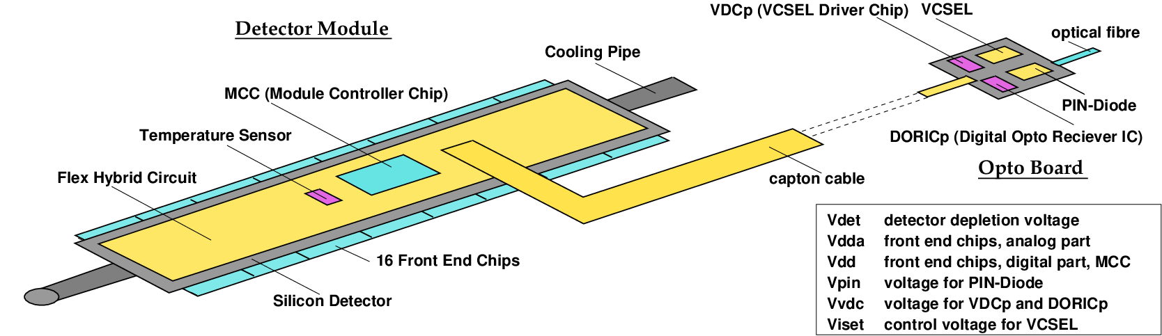
Each detector module (Figure 1) consists of 16 frontend chips which are connected to the associated sensor cells. The readout and control of the frontend chips is provided by the Module Controller Chip (MCC). The analog part of the frontend chips is separately supplied, while their digital part is supplied together with the MCC.
During operation of a detector module, it is also necessary to provide a depletion supply channel for the sensor. In addition, the detector module will have a thermistor (NTC11 1 NTC: negative temperature coefficient) which is used to provide temperature information for each detector module. This thermistor, with a related interlock circuit [1], is used to prevent damage to the hardware due to high temperatures.
2 The Read out Chain
For the data stream between the detector and the read out system an optical transfer for most of the distance of about 80 m will be used.
An opto board is used on the on-detector side to convert the electrical signal into optical signals and vice versa (Figure 2). The supply of this opto board is handled by the SC-OLink22 2 SC-OLink: Supply and Control for the OptoLink which is, like all of the supply components, placed outside the detector volume.
The control of the detector modules, the data taking, and the histogramming of the data is handled by a ROD 33 3 ROD: Readout Driver. On its back, a BOC44 4 BOC: Back of Crate card picks up the optical transmitter Tx, the receiver Rx, and the S-Link card. Inside the counting room, up to 16 ROD/BOC combinations are placed inside a VME crate together with a single board computer which handles the data stream.
3 The Embedded Local Monitor Board
The ELMB55 5 Embedded Local Monitor Board, developed by the ATLAS DCS group, is a multi purpose, low cost I/O device to monitor and control various hardware components [2]. Each ELMB provides up to 64 multiplexed ADC channels and 24 digital I/O-lines. Its CAN66 6 Controller Area Network bus interface and an OPC77 7 OLE for Process Control server provided by the ATLS DCS group allow the integration into the higher level DCS software.
One group of required channels in the pixel DCS accounts for the large number of temperature sensors that are used throughout the detector volume. The majority of those is formed by the detector module thermistors. Additionally the monitoring of the environment and of other temperature sensitive components needs more ADC channels. All devices are equipped with 10 k negative temperature coefficient thermistors and their ead out is based on the use of the ELMB. The control of our custom made DCS hardware is based on the usage of the ELMB (see below).
4 Power Supply System
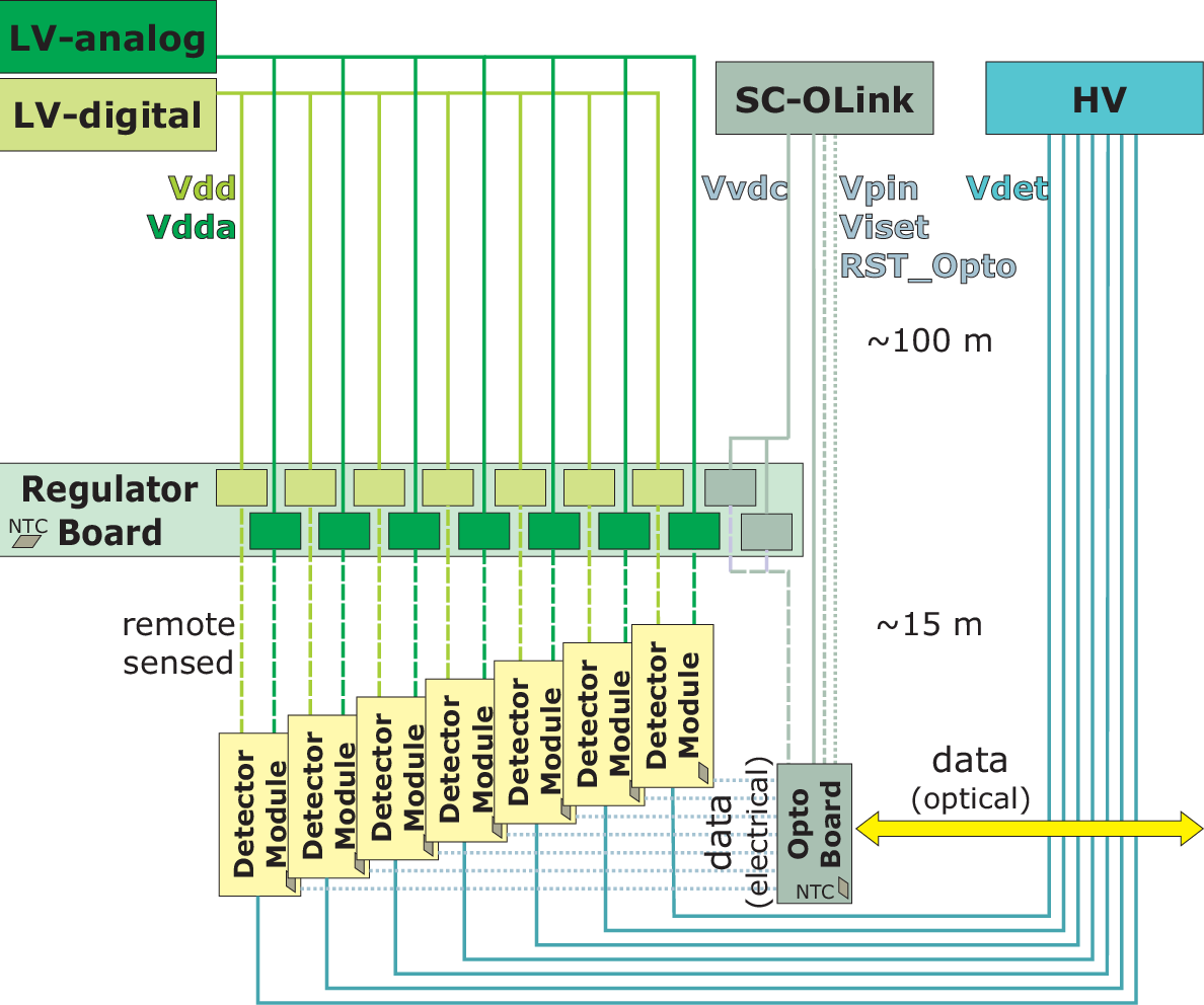
The power supply system has to provide floating channels to be compatible to the ATLAS grounding scheme. Additionaly the outputs should be adjustable over the full range. A high granularity is aimed for to keep the number of operating elements as high as possible.
To provide the supply of the detector modules, commercial power supplies will be used. They will be placed outside the detector volume (off-detector) in the ATLAS counting rooms. Therefore, the services need to be longer than 100 m, and additional devices are required to provide an regulated input for the low voltage channels with higher current to the devices (Figure 2).
To deplete the sensors an iseg88 8 Rossendorf, Germany EHQ F007n-F with 16 outputs will be used. In the beginning of the experiment one channel will supply 6 or 7 detector modules of a sector or a half-stave. In case of increased leakage current inside the sensors due to radiation damages, the modularity will be reduced during the lifetime of the experiment.
For the low voltages (analog and digital) a WIENER99
9
Burscheid,
Germany power supply will provide these, using 2 channels to supply 6 or 7
detector modules (corresponding again to a sector or a half-stave). An active
regulation station [5] inside the detector volume will be used
to regulate the 2 x 6 or 2 x 7 needed voltages for the whole
sector or half-stave using remote sensing.
4.1 The Supply and Control for the OptoLink

Supplying the opto board will be done by the SC-OLink developed by the Wuppertal DCS group [5], each opto board having its separate power supply outputs. Its design is based on the use of the ELMB whichs allows to control a high number of channels economically priced.
The SC-OLink provides two low current channels (20 V and 5 V, 20 mA
each), one 10 V 800 mA channel, and one reset signal. Each of the output
channels uses a separate transformer input to achieve a galvanic separation.
The monitoring of the voltages and currents are separated from the measurement
circuit by using linear opto couplers. The precision for the channels is
better than 8 bit for the output as well as for the monitored values. On the
digital side the used DACs1010
10
DAC: Digital Analog
Converter MAX 5122 are controlled by a
SPI1111
11
SPI: Serial Peripheral Interface,
synchronous serial bus, each one is separated through opto couplers.
The 10 V 800 mA channel does not use remote sensing, as it will be
adjusted by the regulator station using two regulators for redundancy.
4.2 The Regulator Station
To protect the frontend chips, which are fabricated in deep-submicron technology, against transients, remotely programmable regulator stations are installed as close to the detector modules as possible. This radiation hard system has been developed by the INFN Milano group[5]. The regulators compensate for the large voltage drops on the low mass cables in the detector active volume. In parallel they provide an individually adjustable control of the low voltage lines for each detector module. The core of the system is an ST regulator LHC4913 from ST Microelectronics 1212 12 Catania, Italy, which can provide a maximum current up to 3 A and accepts input voltages up to 14 V. Using digital trimmers, the output voltages can be adjusted. The control is based on an FPGA (XC4036XLA-09HQ240C) from Xilinx1313 13 San José, USA, while the communication to the outer world is established by ELMBs.
5 The Detector Control System
The DCS1414 14 DCS: Detector Control System is based on the development environment PVSS II of the Austrian company ETM1515 15 Eisenstadt, Austria and will be used in all LHC experiments to build up the SCADA1616 16 Supervisory Control And Data Acquisition systems. It enables the developer to establish all necessary connections to the supply and protection system. To give the shifters an overview over the system status, and to allow them to operate the system, the DCS provides an easy to use graphical user interface.

The core of the detector control system consists of two major parts (Figure 4): front end integration (power supplies, sensors…) and detector integration (detctor modules, half staves…). It is supplemented by the communication with the data taking system and a finite state machine to simplify the control, which is currently under development.
5.1 The Frontend Integration Tools
To establish the connection to the front end hardware, the FITs 1717 17 FIT: Frontend Integration Tool are used. Besides being the underlying layer for all other hardware DCS components, the FIT also provides panels to monitor and control the connected front end devices (functional approach). Due to the rapidly changing test conditions, especially concerning changing front end hardware, a flexible solution for the FIT was needed. This was realised by implementing a separate FIT for each frontend device like the iseg power supplies or the ELMB.
Additional FITs are being implemented to provide driver functionality for the WIENER power supplies and the regulator stations which still had to be monitored and controlled separately at the system test in 2005. Using the DDC data transfer (see below), a FIT for the BOC is currently under development.
5.2 The System Integration Tool
The mapping of the channels to the detector devices (Figure 4) is done by the SIT1818 18 SIT: System Integration Tool, which has a geographical structure. While relative small test setups only require a limited number of hardware connections (cabling), it will be impossible to manage all 35000 connections of the final detector using a functional approach. Once the physically connected hardware is connected to the DCS using the FIT, the SIT will create a virtual image of the detector inside the DCS. This image will then be used to navigate through the detector’s geographical structure and to monitor and control the relevant data. The system therefore allows for operation of the DCS without deeper knowledge of the physical cabling, which was also tested at the system test.
5.3 The DAQ-DCS Communication
During the experiment, the DAQ1919 19 DAQ: Data Ac quisition system will not only be responsible for taking physics data but also for starting and stopping of runs. On the other hand, DCS has to react correspondingly to ensure correct detector operation. Therefore it is necessary to synchronize the DAQ system with DCS.
For the synchronisation DDC2020 20 DDC: DAQ DCS Communication will be used[4]. The DCS structure will follow the DAQ hierarchy, and on the bottom of the hierarchy the connection between DAQ and DCS will be established. The existing DDC package allows for the bidirectional transfer of data, for the transfer of messages from DCS to DAQ, and for the transfer of commands from DAQ to DCS.
6 The System Test
The aim of the established system test is to validate the concept of the overall design consisting of the power supply and detector control system as well as of the data acquisition system. Interactions between the various components were investigated. Of special interest are studies concerning noise and crosstalk, which could be introduced by the power supply system, the long services, or by the common mechanical structures. It consists of a bi-stave mounted inside a cooling box to ensure controlled environment (regarding temperature and humidity) and to protect the detector modules against light.
6.1 Environmental Control
To avoid condensation on the staves, the cooling box is flushed with nitrogen. Temperature and relative humidity in the cooling box are monitored and used to determine the dewpoint which is calculated with the Magnus [6] formula. The actual dewpoint is the input of a PVSS-script based on a PID controller2121 21 PID controller: Proportional-Integral-Derivative controller, standard feedback loop component in industrial control applications. It determines the control variable dependent on the deviation from the set point, the sum of the deviations and the rate of change of the deviation. The control variable is the input current of a mass flow controller which regulates the nitrogen flow through the cooling box. The current of up to 200 mA is provided by a modified SC-OLink card operating as a current source supply.
The aim was a fast falling of the dewpoint below the setpoint. Once it is below the dewpoint it should stay there without the need of constant, manual adjustment of the nitrogen flow. Further the flow rate should be minimized to reduce the hereby introduced heat.
With the PID control and additional implemented alert handling it is now possible to operate the system test without the need of an operator.
6.2 The Power Supply System
The supply of the system test setup is based on the components introduced in chapter 4. All power supplies and the regulator station are used. Additionally one half stave is equipped with services as they will be used in the final experiment. Their characteristics, including their length, meet the properties as requested for ATLAS.
The main difficulties during the installation and test of the system were caused by ground loops. It turned out that due to the long services potential differences could be built up which made the involved electronics non-operating (Figure 8). This effect made impact on the design of the regulator station and the SC-OLink. The monitoring circuits were therefor equipped with linear opto couplers which guarantee in all conditions a floating range larger than the required 10 V.
6.3 The Read out System
The data path is also geared to the one used in the ATLAS experiment. An optical data transfer to the ead out crate is established. The DAQ software (STcontrol2222 22 STcontrol: System Test control) developed by the Bonn group is based on libraries of the ATLAS DAQ, as they are available at the moment.
6.4 Procedure of the System Test
To evaluate the performance of the whole setup, several tests for the digital and the analog part of the the frontend electronics were enforced for each detector module in several states. Starting at the assembly of a detector module down to the final state when mounted on the stave and integrated in the system test environment, all these tests together allow a rating of the detector module’s performance.
Altogether we got results from four different tests for comparison. The first two are using the well understood laboratory setup, as used during production qualification. It is based on laboratory power supplies with remote sensing, short services and an electrical read out.
- Module Assembly
-
- the individual detector module is measured directly after its assembly with the laboratory setup
- Stave Assembly
-
- after mounting all detector modules on the stave the perfomance of each detector module is verified using again the laboratory setup
The last two results, obtained in the system test (ST), are all based on the system foreseen for the final experiment, which was built up for the first time in its complexity. The power supply system and the optical ead out chain as previously described were used together with long, realistic services.
- ST separate operation
-
- each detector module of the stave is operated individually using the final setup
- ST parallel operation
-
- parallel operating of six detector modules on a stave using the final setup
6.5 Results
All data scans were performed with the configuration of the read out chips determined during the assembly tests. This avoids impacts on the results due to differences in the quality of the tuning. The disadvantage of this procedure is the temperature dependency of the results of the analog scans.
6.5.1 Digital
The digital part showed no effect to the different states, but it was never considered as the critical part sensitive to crosstalk.
6.5.2 Analog
The behaviour of the threshold (Figure 5) shows a correlated behaviour for all detector modules for each state. Obviously the threshold is also correlated to the operating temperatures (Module Assembly @ 25 ∘C, Stave Assembly @ 27 ∘C, ST separate operation @ 18 ∘C and ST parallel operation @ 20 ∘C), it raises with the temperature.

As only one configuration was used and the threshold of the pixel cells are non-uniformly temperature dependent, the threshold dispersion (Figure 6) increases with the difference between the tuning temperature and the operation temperature.

The noise (Figure 7) is only dependent on the absolute temperature of the electronics and shows no other effect as would be expected for a potential crosstalk.

7 Summary and Outlook
A system test utilizing powering and services as foreseen to be used for the ATLAS experiment has been constructed, and has provided valuable first operational experience. The detector control system successfully ensured stable operation of the system. The grounding scheme envisioned for the experiment has been studied extensively, resulting in a modified design for some components of the power supply system.
The experience gained thus far from operating the system test setup indicates that the system of power supplies foreseen for the experiment, as well as the optical readout chain, operate as desired and introduce no problematic effects to the system. This has been verified by operating single modules as well as several modules in parallel, where no deleterious influence has been observed.
The only observable influence was due to the different temperatures of operation. To compensate for the correlation of the threshold dispersion, the detector modules will be tuned again for a set of different temperatures. This should allow a direct comparison for one configuration.
Another remaining objective is to scale up the number of detector modules operated in parallel to check for crosstalk due to the additional hardware and services introduced, as well as to demonstrate the scalability of the readout system and the detector control system.
8 Acknowledgments
For building up and debugging of the system test setup, the knowledge and encouragement of all participating institutes - especially of the ATLAS pixel community - were necessary. The cooperation was highly productive. Thanks to all involved colleagues.
References
- [1] S. Kersten and P. Kind, ’Technical Description of the Interlock Box and Circuit’, ATL-IP-ES-0041, available from https://edms.cern.ch/document/326852/1.0
- [2] ATLAS DCS,’Home Page of Embedded Local Monitor Board’, http://elmb.web.cern.ch/ELMB/ELMBhome.html
- [3] T. Flick et al., ’Optical read out in a Multi-Module System Test for the ATLAS Pixel Detector’, Proc. Pixel2005, Bonn, September 2005
- [4] M. Imhäuser et al., ’First experiences with the ATLAS Pixel Detector Control System at the Combined Test Beam 2004’, Proc. Pixel2005, Bonn, September 2005
- [5] J. Schultes et al., ’The Power Supply System for the ATLAS Pixel Detector’, contribution to the IEEE NSS/MIC conference 2004, Rome, Oktober 2004
- [6] D. Sonntag und D. Heinze, ’Sättigungsdampfdruck- und Sättigungsdampfdichtetafeln für Wasser und Eis.’ (1. Aufl.), VEB Deutscher Verlag für Grundstoffindustrie, 1982
