Three-dimensional isotropic perfect lens based on LC-loaded transmission lines
Abstract
An isotropic three-dimentional perfect lens based on cubic meshes of interconnected transmission lines and bulk loads is proposed. The lens is formed by a slab of a loaded mesh placed in between two similar unloaded meshes. The dispersion equations and the characteristic impedances of the eigenwaves in the meshes are derived analytically, with an emphasis on generality. This allows designing of transmission-line meshes with desired dispersion properties. The required backward-wave mode of operation in the lens is realized with simple inductive and capacitive loads. An analytical expression for the transmission through the lens is derived and the amplification of evanescent waves is demonstrated. Factors that influence enhancement of evanescent waves in the lens are studied and the corresponding design criteria are established. A possible realization of the structure is outlined.
I Introduction
In recent literature a lot of attention has been given to systems that are able to sense electromagnetic near fields (evanescent waves) and even to “amplify” them. The superlens proposed by PendryPendry is one of such systems. His superlens is based on a Veselago mediumVeselago slab. The real parts of the permittivity and the permeability of the Veselago slab are both negative at a certain wavelength. Thus, the eigenwaves in the slab are backward waves, i.e. the wave phase and group velocities are antiparallel. This provides negative refraction and focusing of waves in a planar slab, as was outlined by Veselago.Veselago However, Pendry discovered that there was also a possibility to excite surface plasmon-polaritons on the slab surfaces and, due to that, amplify near fieldsPendry. The slab thickness can be of the order of the wavelength, so that the plasmon-polaritons excited at both sides of the slab are strongly coupled. Under certain conditions the plasmon-polariton excited at the back surface of the slab has a much stronger amplitude than that at the front surface. Such amplification of evanescent waves is the key principle in subwavelength imaging.
Known experimental realizations of volumetric artificial materials with negative parameters are highly anisotropic structures that utilize dense arrays of parallel thin conducting wires and variations of split-ring resonatorsscience. Proposed isotropic arrangements use orthogonal sets of split ringsGay and also three-dimensional arrays of wiresiso. At the same time, there have been achievements in modeling of Veselago materials (and Pendry lens) with the help of -circuits or transmission-line (TL) based structures.Eleftheriades; history; Sanada; Grbic1; Grbic2; Grbic3 These networks do not rely on resonant response from particular inclusions, and the period of the mesh can be made very small as compared with the wavelength. These features allow realization of broadband and low-loss devices, which is extremely difficult if resonant inclusions are used.
The transmission-line network approach has been successfully realized in one- and two-dimensional networks, but up to now there have been doubts if it is possible to design a three-dimensional (3D) circuit analogy of the Veselago medium. The difficulties arise from the fact that such a 3D network requires a common ground connector. Any realization of such a ground will effectively work as a dense mesh of interconnected conductors that blocks propagation of the electromagnetic waves practically the same way as a solid metal does (the structural period must be much less than the wavelength in order to realize an effectively uniform artificial material). In this paper we introduce isotropic three-dimensional transmission-line networks that overcome this difficulty.
In the TL-based networks that we study, the electromagnetic energy propagates through TL sections. The inside of every TL section is effectively screened from the inside of the other sections and from the outer space. This can be very naturally imagined with a 3D cubic-cell network of interconnected coaxial cable segments: The inner conductors of the segments are soldered at the network nodes; the same is done for the outer conductors. The whole system appears as a 3D pipe network where every pipe holds a central conductor and those conductors are crossing at the node points inside the pipes. A loaded TL network can be realized now by placing loading elements inside the “pipes”. To couple the waves propagating inside the TL sections with the free-space waves one will have to apply a kind of antenna array with every antenna feeding a particular TL segment.
When using transmission lines loaded with bulk elements we speak of waves in the meaning of discrete waves of voltages and currents defined at the loading positions. Let us note that in the TL sections as such the usual, forward waves propagate. Only because of the loading the discrete voltage and current waves appear as backward ones when appropriate loading impedances are used.
While completing this manuscript, we learned about another possible design of a 3D transmission-line analogy of a backward-wave material described in Ref. 12. That design is based on Kron’s formal representation of Maxwell’s equations as an equivalent electric circuit.Kron In Ref. 12 only 1D propagation was studied analytically and 3D properties were analyzed numerically.
II Three-dimensional transmission-line networks
The proposed structure of 3D super-resolution lens consists of two forward-wave (FW) regions and one backward-wave (BW) region. The 3D forward-wave networks can be realized with simple transmission lines and the 3D backward-wave network with inductively and capacitively loaded transmission lines. One unit cell of the BW network is shown in Fig. 1 (the unit cell enclosed by the dotted line). In the 3D structure there are impedances Z/2 and transmission lines also along the -axis (not shown in Fig. 1). In view of potential generalizations, the loads are represented by series impedances Z/2 and shunt admittances Y, although for our particular purpose to realize a backward-wave network, the loads are simple capacitances and inductances. The unit cell of the FW network is the same as in Fig. 1 but without the series impedances and shunt admittance . The equations that will be derived for these structures can be used in various implementations, but this paper will concentrate on the case when and .

III Dispersion in backward-wave and forward-wave networks
III.1 Dispersion equations
First we will derive the dispersion relation for a simplified 3D BW network, i.e. we will not take into account the transmission lines. Such approximation is possible at low frequencies. Without the transmission line segments this derivation is quite simple and can be done by summing up all the currents that flow to the node () and equating this sum with the current flowing to the ground (through admittance ), see Fig. 1. The result is
| (1) |
We look for a solution of the form (), and if we use , and , (1) can be reduced to
| (2) |
or
| (3) |
If we now insert and we get the dispersion relation for the LC-loaded network:
| (4) |
Next we want to take the transmission lines into account. The effect of the transmission lines can be derived by first evaluating a part of the three-dimensional network as the one shown in Fig. 2 and deriving the relation between the current that flows into a node and the voltages of adjacent nodes.

If current is flowing towards node () and the current that goes into node () from the left is , then using the ABCD-matrix for a transmission line we get:
| (5) |
| (6) |
where
| (7) |
in (7) is the wavenumber of waves in the transmission lines. From (5) and (6) we can solve and as functions of and :
| (8) |
| (9) |
Similarly for and we get:
| (10) |
| (11) |
Next we can derive two equations for the current flowing through the series impedance and solve from both of them:
| (12) |
| (13) |
| (14) |
| (15) |
If we let in both equations be equal, we can solve as a function of and :
| (16) |
In order to derive an equation for [the current that flows into node () from the direction of node ()] as a function of and , we insert (16) into (11) and get
| (17) |
If we use and , then . Because of the symmetry we can derive the dispersion relation exactly the same way as in (1) – (4), and for the case , the result is
| (18) |
where
| (19) |
| (20) |
III.2 Typical dispersion curves
Dispersion curves for backward-wave and forward-wave networks can be plotted if the values of the transmission line parameters and L and C are fixed. Let us choose the parameters of the TLs and the lumped components as: nH, pF, m (the period of the network), Ohm, Ohm (characteristic impedances of the TLs). See Figs. 3 and 4 for examples of dispersion curves when a -directed plane wave is considered (i.e. ). , where is the speed of light in vacuum. Notice that the BW network supports backward-waves only in the region where 0.32 GHz0.98 GHz. Above that frequency band and the following stopband, the BW network works as a normal FW network until the next stopband appears.


By tuning the capacitance (or inductance ), the stopband between the BW and FW regions shown in Fig. 3 can be closed, see Fig. 5a, where pF. As can be seen from Fig. 5b, by changing the value of from this “balanced” case, the stopband is formed either by moving the edge of the FW region up () or by moving the edge of the BW region down ().

IV The characteristic impedances of backward-wave and forward-wave networks
Next the characteristic impedance of the backward-wave network is derived. If we assume that the interface between the two networks is in the center of capacitor C (see Fig. 2, where ), then we can define the characteristic impedance as
| (24) |
First we have to express , and (or optionally ) as functions of and . We can use equations (14) – (16). If we insert (16) into (15) and (14), we find , and as functions of and . Therefore we can present , and simply as: , and .
Because for a wave moving along the -direction, the characteristic impedance can be expressed as
| (25) |
where
| (26) |
| (27) |
| (28) |
| (29) |
| (30) |
| (31) |
To derive the characteristic impedance of the forward-wave network, we can use the equations derived for the backward-wave network if we insert in them. If this condition applies, we get from (25) – (31):
| (32) |
where
| (33) |
| (34) |
| (35) |
| (36) |


and can be plotted from (25) and (32) as functions of the frequency if the transmission line parameters and L and C are fixed. Let us choose the parameters of the TLs and the lumped components as: pF, nH, m, , Ohm, Ohm (characteristic impedances of the TLs). See Figs. 6 and 7 for examples of the characteristic impedances when a -directed plane wave is considered (i.e. ). The effect of changing on the characteristic impedance can be seen in Fig. 6, and the effect of changing on the characteristic impedance is shown in Fig. 7. Notice that for the BW network the characteristic impedance is continuous only in the “balanced” case ( pF here), because in the stopbands the real part of the impedance is zero.
V Matching of forward-wave and backward-wave networks
We consider a perfect lens with axis parallel to the -axis. To have perfect imaging, the lens should support all spatial harmonics (i.e. waves with all possible transverse wavenumbers ) of the source field and for those values of , and should be equal in magnitude but opposite in sign.
From Fig. 8 we can conclude that the matching of and (which corresponds to a relative refraction index of ) can be achieved only at one frequency (depending on the parameters of the forward-wave and backward-wave networks). In Fig. 8 this frequency is GHz. At this frequency the dispersion curves of the forward-wave and backward-wave networks intersect. In the analytical form this means that
| (37) |
as can be seen from (18) and (23). The dispersion curves in Fig. 8 are plotted so that and are zero (a plane wave moving along the -axis). From Fig. 8 it is seen also that for GHz when . This means that the absolute value of the maximum wavenumber for propagating waves is approximately m-1.

In addition to matching the wavenumbers (refractive indices), to realize an ideal “perfect lens” the interfaces between the forward-wave and backward-wave networks should be also impedance-matched. If the two regions would not be matched, reflections from the interface would distort the field patterns both inside and outside the lens. As can be seen from Figs. 6 and 7, the characteristic impedances of the backward-wave network and the forward-wave network are about 40 Ohms at the frequency where the wavenumbers are matched (and when pF and Ohm). Notice that the impedances of the transmission lines in the forward-wave network have been lowered from 85 Ohm to 70 Ohm to achieve impedance matching of the forward-wave and backward-wave networks.
Next the effect of nonzero on the matching is considered (at the optimal frequency). The minimum and maximum values of can be found from and . From (18) and (23) we can plot and as functions of the transverse wavenumber () if we fix the frequency. Now and are surfaces with variables and . By comparing these surfaces, it was seen that they are practically the same for all possible values of . This happens only at the frequency GHz, where the dispersion curves of the forward-wave and backward-wave networks intersect.
Because the characteristic impedances are functions of the ABCD-matrices and (and is a function of ), we can plot and as functions of if we fix the frequency. Now and are surfaces with variables and . By comparing these surfaces, it was seen that they are almost the same (less than one percent difference) for all possible values of at GHz. See Fig. 9 for a 2D cut of relative difference between such surfaces (now and therefore ). The ideal “perfect lens” situation is achieved with Ohm, as can be seen also from Fig. 9.

When the frequency deviates from the optimal value (for which (37) is true), the wavenumbers and characteristic impedances are no longer matched. The effect of this is distortion of the image seen in the image plane of the lens.
VI Transmission of the source field through the lens
The transmission coefficient of the lens can be solved by considering the incident and reflected fields in the lens system. Let us assume that the incident field outside the lens has the unit amplitude, the reflected field outside the lens has amplitude , the incident field inside the lens has amplitude , and the reflected field inside the lens has amplitude ( is the distance from the front edge of the lens). From these values we can form the following equations (the length of the BW slab is and the transmission coefficient of the BW slab is , see Fig. 10):
| (38) |
| (39) |
| (40) |
| (41) |

The resulting equation for the transmission coefficient is:
| (42) |
The total transmission from the source plane to the image plane (see Fig. 10) is then (distance from source plane to lens is and distance from lens to image plane is )
| (43) |
The longitudinal wavenumber as a function of can be found from the dispersion relations. Let us choose and so we can plot curves instead of surfaces. as a function of can now be plotted if the frequency is fixed. Let us choose the lengths of the lens system as the following: m, m, m. Now we can choose the frequency at which we want to calculate .
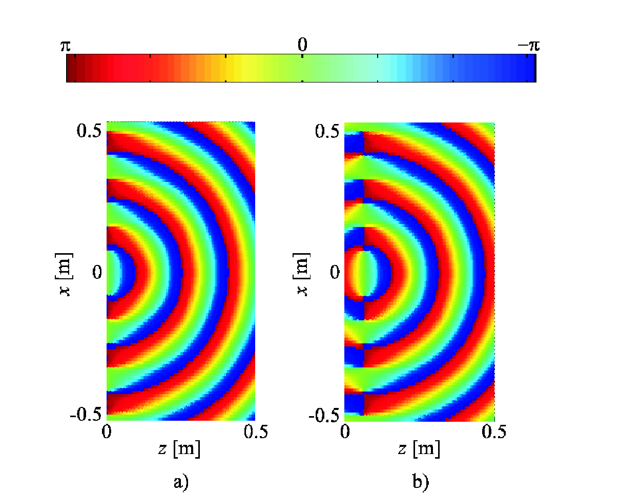
Let us study the transmission properties at the matching frequency GHz. From (42) and (43) we can plot the magnitude and phase of as a function of , see Fig. 11, case 1. From Fig. 11 it is seen that the “lens” works quite well for the propagating modes ( m m-1), see Fig. 12 for an example of phase correction in the image plane.

According to Fig. 11, for evanescent modes ( m m-1) the “lens” works only in a limited range of , where the absolute value of the transmission coefficient is greater than zero. One can notice that for evanescent modes a mismatch in affects mostly the phase of in the area of propagating waves and a mismatch in the characteristic impedances affects primarily the absolute value of . To improve the effect of evanescent waves enhancement, the characteristic impedances should be matched better in the evanescent wave area of (i.e. m m-1). There are several ways to achieve a better matching of the characteristic impedances.
First, there is of course a possibility to change the impedances of the transmission lines, but this is probably not practically realizable because it would require very accurate manufacturing (even a very small deviation from the ideal impedance values destroys the effect of growing evanescent waves). The tuning of was tested and using the exact impedance required (see Fig. 9), the transmission of evanescent waves was clearly improved. The resonance peaks in Fig. 11 were moved further away from the center and the absolute value of was larger than or equal to unity approximately for m m-1).
Second, there is a possibility to change the frequency and study if the impedance matching can be made better that way (this also means that the matching of wavenumbers is made worse which can also destroy the effect of growing evanescent waves). This was tested and the best results were obtained using frequency GHz. The region of transmitted ’s was again increased, i.e. the resonance peaks in Fig. 11 were moved further away from the center and the absolute value of was larger than or equal to unity approximately for m m-1).
The third way to enhance the growth of evanescent waves is to change the length of the “lens”. From (42) it is seen that the growth of evanescent waves is destroyed by the term in the denominator. This term can be made smaller by decreasing the length of the “lens” . See Fig. 11, case 2 ( is larger than or equal to unity approximately for m m-1) and Fig. 13, where the distances equal m, m and m. From Fig. 13 one can conclude that there is a significant growth of evanescent waves in the lens.

By using the shortened lens and at the same time tuning the frequency appropriately, it was seen that the transmission coefficient could be made practically ideal (i.e. and for all possible values of ). Using the shortened lens (same values as in Fig. 13) and frequency GHz, the absolute values of evanescent fields were indeed almost the same in the image plane and in the source plane (less than one percent difference).
VII Suggestions for a practically realizable structure
VII.1 Proposed structure
How to manufacture three-dimensional transmission line networks? The main problem is the ground plane, which should exist in all three dimensions. One solution would be to use coaxial transmission lines (regular in the forward-wave network and loaded with lumped L- and C-components in the backward-wave network) as shown in Fig. 14a. This structure is realizable, but we propose a simpler structure based on microstrip lines, as presented in Fig. 14b. The problem with microstrip lines is of course the design of intersections where the transmission lines from six directions meet. This problem can be overcome by using ground planes which have holes in them at these intersection points. This way the conducting strip can be taken through the substrate and thus connection of the vertical conducting strips becomes possible.

VII.2 Simulation results
The proposed structure (see Fig. 14b) has been simulated in Ansoft HFSS (Version 9.2.1). Due to complexity of the structure and the limited calculation power available, the three-dimensional structure was simulated only near the first lens interface of Fig. 10. The simulated model had () unit cells in the forward-wave region and unit cells in the backward-wave region. The properties of the transmission lines and lumped elements were the same as in Fig. 8. The edges of the system were terminated with matched loads to prevent reflections ( Ohm in the backward-wave region and Ohm in the forward-wave region). Different types of source fields (plane waves with different incidence angles and a point source) were tested and in all cases negative refraction was observed at the interface between the forward-wave and backward-wave networks at the expected frequency ( GHz).
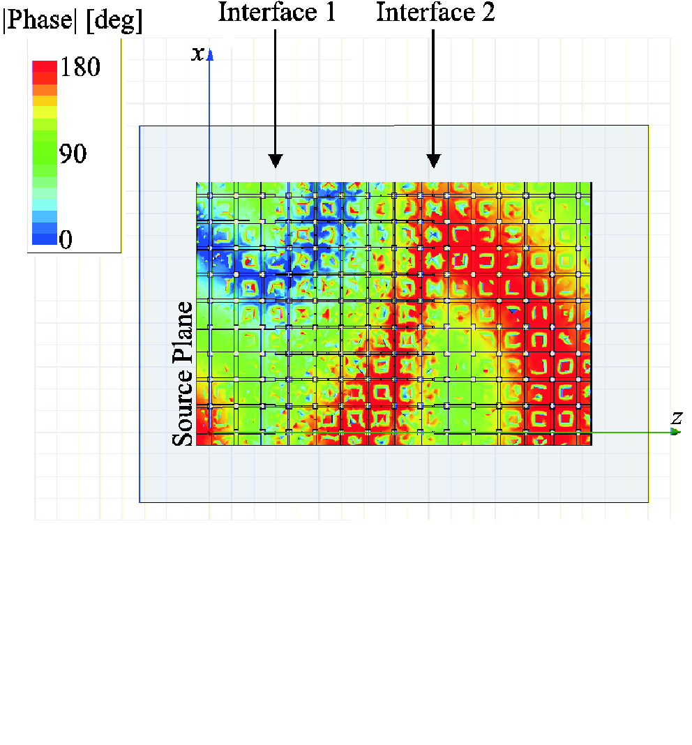
A two-dimensional cut of the proposed structure was simulated as a complete “lens” system. Again negative refraction was seen at both interfaces, and therefore also focusing of propagating waves was observed. See Fig. 15 for the plot of the phase of the electric field in the two-dimensional simulation. The source field is excited at the left edge of the system in Fig. 15. When the field magnitude is plotted and animated as a function of phase, it is clearly seen that the phase propagates to the right in the forward-wave regions and to the left in the backward-wave region. The energy of course propagates to the right in all regions.
VIII Conclusions
In this paper we have introduced and studied a three-dimensional transmission-line network which is a circuit analogy of the superlens proposed by Pendry. The structure is a 3D-network of interconnected loaded transmission lines. Choosing appropriate loads we realize forward-wave (FW) and backward-wave (BW) regions in the network. The dispersion equations and analytical expressions for the characteristic impedances for waves in FW and BW regions have been derived. A special attention has been given to the problem of impedance and refraction index matching of FW and BW regions. From the derived dispersion equations it has been seen that there exist such a frequency at which the corresponding isofrequency surfaces for FW and BW regions coincide. Theoretically this can provide distortion-less focusing of the propagating modes if the wave impedances of FW and BW regions are also well matched. Impedance matching becomes even more important when the evanescent modes are taken into account. In this paper we have shown that the wave impedances can be matched at least within 1% accuracy or better if the characteristic impedances of the transmission lines are properly tuned. However, from the practical point of view an accuracy better than 1% becomes hardly realizable. It has been shown that decreasing the thickness of the BW region reduces the negative effect of the impedance mismatch, while the amplification of the evanescent modes is preserved. We have also outlined a couple of prospective designs of the perfect lens discussed in this paper and numerically simulated their performance.
Acknowledgment
This work has been done within the frame of the Metamorphose Network of Excellence and partially funded by the Academy of Finland and TEKES through the Center-of-Excellence program. The authors would like to thank Dr. Mikhail Lapine for bringing paper Grbic4 to their attention and for helpful discussions.
References
- (1) J.B. Pendry, “Negative refraction makes a perfect lens,” Physical Review Letters, vol. 85, no. 18, pp. 3966-3969, Oct. 2000.
- (2) V.G. Veselago, “The electrodynamics of substances with simultaneously negative values of and ,” Soviet Physics Uspekhi, vol. 10, no. 4, pp. 509-514, Jan. - Feb. 1968.
- (3) R.A. Shelby, D.R. Smith, and S. Schultz, “Experimental verification of a negative index of refraction,” Science, vol. 292, pp. 77-79, Apr. 2001.
- (4) P. Gay-Balmaz and O.J.F. Martin, “Efficient isotropic magnetic resonators,” Applied Physics Letters, vol. 81, no. 5,pp. 939-941, Jul. 2002.
- (5) Th. Koschny, L. Zhang, and C.M. Soukoulis, “Isotropic three-dimensional left-handed metamaterials”, Physical Review B, vol. 71, 121103(R), 2005.
- (6) G.V. Eleftheriades, A.K. Iyer, and P.C. Kremer, “Planar negative refractive index media using periodically L-C loaded transmission lines,” IEEE Trans. Microwave Theory and Techniques, vol. 50, no. 12, pp. 2702-2712, Dec. 2002.
- (7) C. Caloz, H. Okabe, T. Iwai, and T. Itoh, “Transmission line approach of left-handed (LH) materials”, in Proc. USNC/URSI National Radio Science Meeting, San Antonio, USA, vol. 1, p. 39, June 2002.
- (8) A. Sanada, C. Caloz, and T. Itoh, “Planar distributed structures with negative refractive index,” IEEE Trans. Microwave Theory and Techniques, vol. 52, no. 4, pp. 1252-1263, Apr. 2004.
- (9) A. Grbic and G. V. Eleftheriades, “Periodic analysis of a 2-D negative refractive index transmission line structure,” IEEE Trans. Antennas and Propagation, vol. 51, no. 10, pp. 2604-2611, Oct. 2003.
- (10) A. Grbic and G.V. Eleftheriades, “Negative refraction, growing evanescent waves and sub-diffraction imaging in loaded transmission-line metamaterials,” IEEE Trans. Microwave Theory and Techniques, vol. 51, no. 12, pp. 2297-2305, Dec. 2003.
- (11) A. Grbic and G.V. Eleftheriades, “Overcoming the diffraction limit with a planar left-handed transmission-line lens,” Physical Review Letters, vol. 92, no. 11, 117403, Mar. 2004.
- (12) A. Grbic and G.V. Eleftheriades, “An isotropic three-dimensional nagative-refractive-index transmission-line metamaterial,” Journal of Applied Physics, vol. 98, 043106, 2005.
- (13) G. Kron, “Equivalent circuits to represent the electromagnetic field equations,” Physical Review, vol. 64, no. 3-4, pp. 126-128, Aug. 1943.