First principles electron transport: finite-element implementation for nanostructuresPreprint: APS/123-QED
Abstract
We have modeled transport properties of nanostructures using the Green’s function method within the framework of the density-functional theory. The scheme is computationally demanding so that numerical methods have to be chosen carefully. A typical solution to the numerical burden is to use a special basis-function set, which is tailored to the problem in question, for example, the atomic orbital basis. In this paper we present our solution to the problem. We have used the finite element method (FEM) with a hierarchical high-order polynomial basis, the so-called p-elements. This method allows the discretation error to be controlled in a systematic way. The p-elements work so efficiently that they can be used to solve interesting nanosystems described by non-local pseudopotentials.
We demonstrate the potential of the implementation with two different systems. As a test system a simple Na-atom chain between two leads is modeled and the results are compared with several previous calculations. Secondly, we consider a thin hafnium dioxide (HfO2) layer on a silicon surface as a model for a gate structure of the next generation of microelectronics.
pacs
72.10.-d, 71.15.-m, 73.40.-cI Introduction
Using small nano-scale lithographic structures, atomic aggregates and even single molecules, it is possible to fabricate new kind of electronic devices Datta 1995. The function and scale of these devices is based on quantum-mechanical phenomena, and cannot be described within the classical regime. Of particular relevance are the electron transport properties of these nanoscale devices, as this will determine their effectiveness in, for example, a new generation of transistors. As the experimental work on these devices grows, increasing emphasis is placed on developing a matching theoretical description Nitzan 2001; Nitzan and Ratner 2003. Although some efforts have included a full description of an electronic circuit Luo et al. 2002; Kim et al. 2005, current research is mainly focused to study single electronic components.
Density-functional theory (DFT) is widely used in atomistic modeling of materials properties and recently also properties and phenomena in nanostructures. The power of DFT is in its capacity to treat accurately systems with a hundreds of atoms, yet retain a full quantum-mechanical treatment. Although the full justification of use of the DFT in electron transport calculations is debated Burke et al. 2005; Thygesen and Jacobsen 2004 we adopt it as a practical scheme to describe the real systems and devices.
In the Kohn-Sham scheme of DFT the electron density is calculated using single-particle wave functions. The explicit use of the wave functions in constructing the density suffices well in two kinds of systems. Either the system has a repeating structure so that it can be modeled with periodic boundary conditions or the system is so small that it can be calculated as a whole. In nano electronics, however, a system consists usually of a small finite part, the nanostructure, which is connected to the surrounding infinite leads. If one enforces periodic boundary conditions even a large repeating super cell or calculation volume can cause finite-size effects with spurious results for electron transport.
A commonly used solution to this problem, which we have also employed, is to combine DFT with the Green’s function formalism Datta 1995. The Green’s functions are first constructed for the semi-infinite leads by using the analytically known or easily calculated wave functions. Once the Green’s function for the combined nanostructure and leads is constructed, the wave functions are no longer needed explicitly. This makes it possible to use open boundary conditions between the nanostructure and the lead. In this way we have an effectively infinite system without periodicity, making the finite-size effects small. It is also possible to calculate the electric current through the system for a finite bias voltage between the leads in a self-consistent manner with the electron density. The ensuing model for the current is analogous to the Landauer-Bütteker model Nitzan 2001. We have used non-local pseudopotentials for modeling atoms, and the ideal metal “jellium” model for the leads. The charge density in the leads can be varied according to the conducting properties of the leads we wish to model.
The use of Green’s functions instead of the explicit use of wave functions is computationally demanding. This is why special care has to be taken in choosing the numerical methods. The first implementations used tight-binding methods Sautet and Joachim 1988; Chico et al. 1996, but a more typical solution is to expand the Green’s functions in a special basis tailored for the system. Common examples are localized atomic orbitals Taylor et al. 2001; Brandbyge et al. 2002, an optimized basis Nardelli et al. 2001, a wavelet basis Thygesen et al. 2003, full-potential linearized augmented plane-waves Wortmann et al. 2002, maximally localized Wannier functions Calzolari et al. 2004, a finite-difference method Khomyakov and Brocks 2004, and linear a finite-element method Polizzi and Ben 2005. Our solution is to use the finite-element method (FEM). It allows a systematic error control which is especially important in transport problems as there are many different properties which must be monitored. For example, the pole of the Green’s function can cause numerical problems. According to our experience electronic tunneling in particular is sensitive to numerical accuracy.
Besides systematic error control, the FEM has also other good properties which makes it a natural method for transport problems. It is a flexible method which allows one to take into account the geometry of the nano device exactly. Special boundary conditions are easy to derive without mixing the model with the numerical method and their implementation is straightforward. Moreover, the local nature of the basis produces sparse matrices for which efficient solving methods exist. Varying the size of the elements can be used to reduce the number of the basis functions and, consequently, the size of the system as compared to the finite-difference method. This is especially true for the high-order -method. Finally, there exists a lot of theoretical work together with tested and reliable tools, such as mesh generators and optimized linear solvers. These are used as standard building blocks for any FEM implementation granting easy access to state-of-the-art algorithms. Using the FEM new theoretical or numerical ideas are easy to implement and test.
The structure of the paper is as follows: in Sec. II we describe the model itself in detail, including a discussion of the formalism of our implementation; in Sec. III we apply the model to two example systems, a Na atom chain and HfO2-Si interface between two leads. In Sec. IV we summarize the work. In this paper we use atomic units in all equations.
II Model
The schematic picture of our model is shown in Fig. 1. Actually, the figure present our second test case, the HfO2-Si interface between two leads. We have an atomistic nanostructure between two semi-infinite leads. The system is divided into three parts, being the calculation volume, and and are left and right leads, respectively. The boundaries are open so that electrons can penetrate through them without any reflection or refraction. We use the DFT to model electron interactions. The basic quantity, the electron density, is calculated from single-particle Green’s functions. Then we use the density to calculate the effective potential as

| (1) |
where is the external potential caused by positive background charges, local parts of the pseudopotential operators and the potential outside potential barriers. is the Coulomb Hartree interaction part, and is the exchange-correlation part which we calculate using the local-density approximation parametrized by Perdew and Zunger Ceperley and Alder 1980; Perdew and Zunger 1981. sets the boundary conditions if a bias voltage is applied. is the nonlocal part of the pseudopotential operators.
The Hartree potential is calculated from the modified Poisson equation
| (2) |
where is an adjustable parameter. does not affect the final self-consistent result, but the stability and convergence of iterations are improved Arponen et al. 1973, because the Coulomb potential due to charge redistribution between adjacent iterations is screened. The non-local pseudopotential is an operator given by
| (3) |
where and are defined using the Troullier-Martins pseudopotentials Fuchs and Scheffler 1999; Troullier and Martins 1991. Eq. (3) uses the projection of the function (arbitrary function, which in practical calculations is a basis function) on the atomic-specific function depending on the quantum numbers and corresponding to the angular momentum.
We have implemented the guaranteed-reduction-Pulay Bowler and Gillan 2000 method for the mixing of the self-consistent iterations. It uses potentials from the five previous iterations for computing a new potential in such a way that the predicted norm of the potential residue is minimized. The simplest mixing scheme in which potentials are mixed with a linear feed-back coefficient does not work well in open systems. The calculations are rather unstable so that quite a small feed-back coefficient has to be used. This is because the net charge in the calculation volume varies during the calculations.
II.1 Green’s function model
The details of the Green’s function method for electron transport in nanostructures are explained, for example, in Ref. Xue et al. 2002. Here we give only a short introduction to the equations to be solved. The retarded Green’s function is solved from the equation
| (4) |
where is the electron energy and is the DFT Hamiltonian of the system,
| (5) |
When we know we can calculate the so-called lesser Green’s function . In the equilibrium when no bias voltage is applied over the nanostructure it is obtained from
| (6) |
where are the Fermi functions of the leads. In the equilibrium, . For a finite bias voltage we take into account the bias and a more complicated equation for has to be used. To obtain it we write Eq. (4) in the form
| (7) |
where is the Hamiltonian of the isolated volume and are the so-called self-energies of the leads. We also define
| (8) |
and can solve for a finite bias voltage as
| (9) | ||||
The first and second terms correspond to electrons originating from the right- and left leads, respectively. The electron density is calculated from
| (10) |
and the tunneling probability from
| (11) | ||||
from the values of the functions at the boundaries . Finally the current is determined as
| (12) |
We use the FEM in the numerical implementation. Therefore we first cast Eq. (4) in the variational form with open boundary conditions (for the derivation, see Ref. Havu et al. 2004) as
| (13) | ||||
where the self energy-operators
| (14) | |||
Above, is the Green’s function of the semi-infinite lead in the domain with the zero-value condition on the boundary . In our implementation the leads are described by a uniform positive background charge and therefore can be calculated partly analytically. Thus our model means that the leads are of some kind of ideal generic metals. The important interface between the nanostructure, e.g. a molecule, and the actual metallic lead can be described accurately by including some lead metal atoms in the computational domain . It is also possible to use fully atomistic leads by calculating numerically for them.
Note that the Eqs. (13) and (14) are analogous to those derivations of the open boundary conditions in which truncated matrices Datta 1995 are used. In the continuum limit these two forms give the same results. However, the weak form is more natural in the FEM formulation and more suitable for theoretical purposes when analyzing nonlinear partial differential equations. It is also straightforward to use and the error control is systematic. Note that this formulation can be used with any continuous basis set, not only with the FEM. In the context of basis set methods, the weak formulation case is known as the Galerkin method. In practice the Green’s functions are approximated with respect to this basis so that
| (15) |
The coefficients can be solved from (13) by choosing and evaluating the equations.
II.2 Finite-element p-basis
In the FEM we partition the calculation volume to (in our case, tetrahedral) sub-domains called elements and the basis functions are constructed using globally continuous (but not necessarily continuously differentiable) piecewise polynomials with respect to the finite element mesh. This gives both unique flexibility of the approximating functions as well as completeness of the basis with respect to almost any norm. Each basis function has a support that is concentrated to only a few neighboring elements. This makes the basis local and results in sparse system matrices.
There are several options of how to choose the finite-element basis and one has to be careful in achieving acceptable accuracy. The simplest basis is the linear one. It is easy to implement and works well, especially in systems with rapidly varying functions. A typical improvement to this basis is to use node-based higher-order elements. These elements converge faster to a smooth solution than the linear ones. However, practically only relatively low orders, two and three, can be used because of numerical stability problems.
In this work we have used so-called hierarchical -elements. They also span higher-order polynomials, but the choice of the local basis ensures that stability problems do not appear. This is because the basis functions are chosen so that their derivatives are close to orthogonal in the -norm. The hierarchical nature also makes it easy to change the order of the basis from element to element within the same mesh.
The actual FEM implementation consists of a reference element and reference basis that are mapped separately to each of the elements of the mesh. Our reference element is a tetrahedron with nodes at the coordinates , , and . One can easily show that there exists an affine map taking the reference element to any of the tetrahedron. The order of our basis is meaning that in each element polynomials of the order of are employed. The basis is constructed hierarchically. First, there are four linear node basis functions inside the elements sharing a common node. In the reference element they are
| (16) | ||||
where and are the cartesian coordinates of the reference element. Secondly, for 1 we have edge functions. E.g. for the edge between the nodes 1 and 2
| (17) |
Here one usually sets
| (18) | ||||
Above is the Legendre polynomial of the order of . Third, we have face functions. For example for the face between the nodes 1,2, and 3 they are
| (19) | |||
Fourth, we have bubble functions, which are supported only in a single element each. These are
| (20) | |||
When -elements are used one must take care of the continuity of the basis. This is because, for example, the local basis function has an orientation on the boundary. The basis includes the function , not , which would be another possibility. This means that all the edges in the mesh have to have information about the direction. Otherwise there is very likely a continuity problem on some boundaries. In practice, for tetrahedral elements the orientation problem can be handled for arbitrary finite-element meshes using only two reference elements Ainsworth and Coyle 2003.
The benefits of selecting the basis described above are rather clear. The polynomial basis is very easy to realize and has good approximating properties. For smooth solutions the -basis is known to give exponential convergence rates with respect to the number of basis functions used. In the DFT methods the theory is typically developed to the direction that the solutions are as smooth as possible. For example, pseudopotential operators are designed so that they produce as smooth an electron potential as smooth as possible. This is because the plane-wave basis set needs smooth solutions in order to work efficiently. On the other hand, in the case of non-smooth solutions one can benefit from the piecewise nature of the FEM basis allowing one to approximate even singular solutions to some extent. Moreover, the finite element mesh can be refined in regions where solution changes rapidly. When modeling molecules there is also a lot of empty space in the calculation domain. It is then practical to use large elements in the empty space and smaller ones near atoms.
II.3 Linear algebra methods
The use of the Green’s function method is computationally demanding in comparison to explicit wave-function methods. Since the main computational burden of our method is to find a subset of the coefficients of the Green’s function in question, a special consideration must be taken when choosing the methods of linear algebra to be used. The eigenvalue problems in explicit wave-function methods are typically solved by iterative methods. In our case it is better to use direct solvers, because a set of linear equations needs to be solved. We have opted for the frontal method widely used in the solution of sparse linear systems Reid and Duff 1983; Duff 1996 and extremely suitable for finite-element matrices. The actual implementation is ME47 of the Harwell Subroutine Library (HSL) hsl (see Refs. Gupta 2000; Davis 2004; Demmel et al. 1999 for other similar approaches). In the frontal method, one first finds a permutation of the sparse matrix aiming to minimize the fill-in resulting from the factorization process. Next, a LU-decomposition (or Cholesky-decomposition for symmetric problems) of the matrix is found, and finally, two systems with triangular coefficient matrices, and (where for symmetric problems) are solved. To find all the required coefficients of the solution we must vary the right-hand side of the system.
For a three-dimensional problem the size of the linear system can grow so large that the CPU-time and memory requirements of different systems have to be addressed. The main question is how large systems can be calculated using these methods so that the calculation time for a single self-consistent iteration is not too large. Currently a system of several tens of thousands of unknowns can be solved in a commodity-CPU cluster environment.
In detail, the Green’s function method includes a computation of the elements for the inverse of a sparse matrix, so that the calculation time requirements increase relatively fast with the system size. A classical complexity result for the solution (and inversion) of a general system with a direct method is . However, for sparse systems and modern frontal methods this bound is too pessimistic George and Liu 1981. The CPU time requirement depends on the fill-in of the inversion problem. For very simple cases one can show that the key statistic of the problem, the number of non-zeros (nnz) present in the factors and , satisfies George and Liu 1981. Then the solution of each of the systems requires floating-point operations, and in the worst case we must solve these with different right-hand sides effectively giving us the inverse of the matrix , so that the total cost is . However, in modern computer systems the complexity is not the only relevant measure since the performance may be highly nonlinear (see, e.g. atl; Goto and van de Geijn 2002 for an example on BLAS-tuning).
Another topic related directly to the performance of modern computer systems is the relation between processor power and memory bandwidth. This is especially true for the computation of the Green’s function where the actual bottleneck is the lack of available memory bandwidth in commodity-based cluster systems used in calculations, not the floating-point performance of the processor itself.
It is likely that a better performance can be achieved by upgrading several parts of the algorithms. First, the current parallel solver is implemented using the Message Passing Interface (MPI) mpi. However, in Symmetric multiprocessor (SMP) systems it is likely that well-designed OpenMP ope (or similar) parallelism would reduce the need for data transfer and thus increase performance. It would also decrease the memory requirements of the problems. Second, at the moment the solution of the Green’s function is computed varying one vector on the right-hand side at a time. A better performance could be obtained if the equations could be solved for multiple right-hand sides at a time allowing the use of BLAS3 routines. Finally, it is likely that computations would benefit from a computer system having a larger memory bandwidth than our present commodity-based one.
III Example systems
III.1 Atomic wire
Using the atomic force microscope or the mechanically controlled break junction technique, a chain of atoms can be made of certain metals Agrait et al. 2003. It has been observed that the conductances of atom chains vary as a function of the number of atoms in the chain Smit et al. 2003. The conductances of these systems have been studied also theoretically in several works. In order to benchmark our results against other calculations, we use Na-atom chains as test systems. They have been simulated in several previous studies Sim et al. 2001; Lang 1997; Tsukamoto and Hirose 2002; Lee et al. 2004 using different models. According to these calculations the conductances of the wires show even-odd oscillation as a function of the number of atoms in the wire.
In our setup, the Na-atom chain is located between two leads, with the lead shape defined by a 70∘ cone angle (see Fig. 2). We consider two different connections of the atom chain to the electrodes. In model A we have just three Na atoms between the jellium leads. This resembles closely the system used in Ref. Lang 1997. In model B, there are four Na atoms at the tips of the leads in a square form. This makes the connection between the atom chain and the leads more realistic. This kind of structure is modeled also in Ref. Tsukamoto and Hirose 2002.


The conductances as a function of the number of chain atoms for systems A and B are shown in Fig. 3. In the Na-atom chain, electrons have only one conducting mode so that the conductance can be one conductance quantum at maximum. Both systems A and B exhibit conductance oscillations as a function of the number of atoms. These oscillations arise from resonance states in the atom chain. Depending on the position of the resonances relative to Fermi-level the conductance has either a maximum or minimum value, so that the maxima and minima correspond to approximately half and fully occupied resonance states, respectively. The oscillation is within the range of 0.9 - 1.0 for system A and 0.6 - 1.0 for system B. The difference between the oscillation amplitudes is due to different strengths of the connection of the chains to the leads. System B has a weaker coupling to the leads than system A. Weak connections make the resonances also sharper, as is seen in the tunneling probability in Fig. 4. In contrast to Ref. Havu et al. 2002, we do not see a strong lead-shape dependence in the conductance. The widening of the cone angle lowers the conductance as the edges of the wire become sharper.
The electron tunneling probabilities through chains of three- and four- atom systems A and B are shown in Fig. 4. The probability function is defined in Eq. (11). The conductance of the system in the zero-bias limit can be read at the Fermi-level. Here, as well as in Fig 3, we see that the conductance oscillations for systems A and B are in a different phase. This is because in system B the atom chain is effectively shorter than in A, as the first and the last chain atom are partly inside the square of the four Na atoms.
When we compare the conductance oscillations of system A (see Fig. 3) to those in Ref. Lang 1997 obtained by using semi-infinite jellium leads with planar surfaces (), we see that the even-odd oscillations in the conductance are in the same phase. In the case of system B we can directly compare the tunneling probability of Fig. 4 with those in Ref. Tsukamoto and Hirose 2002 where the atom chain is connected also through a square of four Na atoms to jellium. The phase and the amplitude of the conductance oscillations of these results are in good agreement with our values in Fig. 3. Now that we have satisfied ourselves that the method provides a good model for electron transport we can consider a more interesting and demanding example.
III.2 Thin insulating layer
The general increase in the performance of microelectronic devices in the past few decades has been made possible by continuous transistor scaling - based on a reduction in the thickness of the gate dielectric in typical metal-oxide-semiconductor field-effect transistors (MOSFET). At present the process has reached a bottleneck, as further reduction leads to a large increase in leakage current due to direct tunneling across the thin silicon dioxide (SiO2) layer. Several possible approaches to resolve this are being considered Kingon et al. 2000, but retaining conventional MOSFET design remains an economically attractive choice, and a leading option is just to replace SiO2 with another oxide of higher dielectric constant (high-). A high- oxide would provide higher effective capacitance to a comparable SiO2 layer, hence allowing thicker layers to be used to reduce losses due to tunneling. The specific choice of oxide is determined by a set of requirements Huff et al. 2003 based on both the intrinsic properties of the grown oxide and its integration into the fabrication process, and at present hafnium oxide (HfO2) remains a leading candidate.
In order to study to transport properties of thin HfO2 films we have simulated the growth of the oxide on a silicon surface via first principles molecular dynamics Hakala and Foster 2005. Here we consider three model interfaces: (i) a nonstoichiometric oxide interface (C), which is basically metallic due to Hf-Hf and Hf-Si bonds across the interface; (ii) a stoichiometric oxide interface ( D), which has a localized state in the band gap due to a few Hf-Hf bonds; (iii) a more idealistic interface (E), which remains insulating if no defects are present. The last model is based on the interface used in Ref. Fonseca et al. 2003, but slightly reduced in size to make it computationally manageable Gavartin et al. 2005. These models were calculated with periodic boundary conditions with k-points on the boundaries . The effective potentials have been calculated for systems C and D using the gamma point, and for system E, four -points. All the tunneling probabilities are calculated using four -points, which was enough to converge the probabilities to a good accuracy.
As shown in Fig. 1, the interface models are positioned between two leads. The charge density in the leads is chosen so that in the right lead (electron density ), representing a metal, and in the left one , representing doped-silicon - as in a standard MOSFET design.

The tunneling profiles of the systems are shown in Fig. 5. Here it is seen that systems C and D show clearly metallic behavior, with a large tunneling probability at the Fermi energy. Although in principle, the stoichiometric interface (D) has a much lower density of metallic bonds, it is clear that both in interfaces C and D around two channels dominate the transport. The localized defect state in the band gap of system D plays an equivalent role in transport to the metallic bonds in interface C.
As expected, the tunneling probability for the more ideal interface E is an order of magnitude smaller at the Fermi energy than those for interfaces C and D. Yet we also see that it remains significant - this is largely due to the structure of the interface itself Fonseca et al. 2003. Although bulk HfO2 is a wide-bandgap insulator, at the interface it exists as almost tetragonal HfSiO4, and the effective band gap is actually smaller than that of bulk silicon below the interface. This means that there is a negative conduction band offset between silicon and HfO2, and no real barrier for leakage. Although some of this is caused by the underestimation of the band gap in the DFT, this also reduces the silicon band gap (although the effect is not systematic).
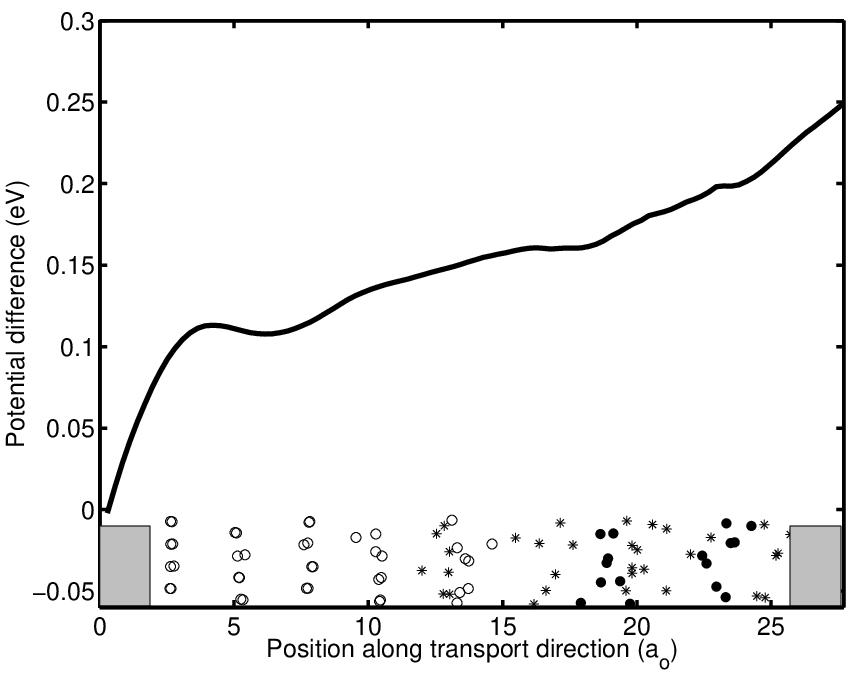
The poor performance of interface D can also be seen in its capacity for dropping the potential. Fig. 6 shows the potential change for 0.25 V applied bias voltage. The potential drop across HfO2 is less than 0.05 eV, demonstrating that the oxide hardly perturbs the electron flow from the right lead. The potential drops fastest at the right hand side of HfO2-layer where pure HfO2 exists, and much more slowly in the thin layer of SiO2 formed due to diffusion of oxygen. The large drop at the lead and silicon atoms is just an artifact of the boundary conditions of the Coulomb part of the effective potential.
In the rigid band approximation (used for example in Ref. Fonseca et al. 2003) it is assumed that the shape of the tunneling probability stays constant and is only shifted in energy so that , where is the ratio of potential drop at the other end of the nanostructure to the total drop over the nanostructure. In Fig. 7 we have studied how well this approximation works for interface D. The curves are plotted so that the zero-bias Fermi level is in the middle of the left and right Fermi levels of the biased interface. This corresponds to the symmetric case with . We see that the tunneling probability curves roughly coincide. This indicates that potential drops symmetrically over the nanostructure and the rigid-band approximation gives a rather reasonable result.

The above results show, in agreement with previous calculations Fonseca et al. 2003 that tunneling through a more ideal, insulating interface is still significant due to a negative band offset with silicon. Since the only HfO2 interfaces providing significant band offsets to silicon were built very idealistically (i.e. assuming no significant atom migration nor interfacial SiO2 growth) Fiorentini and Gulleri 2002; Peacock and Robertson 2004, this indicates that fabricating a good interface directly between silicon and HfO2 is very difficult. A more viable alternative maybe to sacrifice somewhat in dielectric constant, and grow HfO2 onto a pre-existing SiO2 layer. These possibilities will be explored in more detail in a further work Hakala and Foster 2005.
IV Conclusions
In this paper we present a finite-element implementation of the non-equilibrium Green’s function method which is combined to the density-functional theory. Although the Green’s function method is computationally demanding, we demonstrate that by using hierarchical -elements, large, physically relevant systems become tractable. More importantly, our method offers a much more rigorous control of accuracy than is usually possible in transport calculations.
We demonstrate the functionality of our implementation with two kinds of systems, the sodium atom chain wire and the silicon-HfO2 interface. For the atom chain, we show that the method reproduces the previous results of other Green’s function transport methods. This gives us confidence to apply it to the more complex system: a thin layer of hafnium oxide on a silicon substrate. Here we show that the transport properties are an even more sensitive indicator of the role of defects than the electronic structure. Comparison of stoichiometric and non-stoichiometric HfO2 oxide layers demonstrates that even one or two defects in a stoichiometric interface can result in tunneling comparable to that of a fully metallic non-stoichiometric interface.
Acknowledgements.
We are grateful to J. L. Gavartin and L. R. C. Fonseca for providing us with access to their interface structures, and for helpful discussions. We acknowledge the generous computer resources from the Center for Scientific Computing, Espoo, Finland. This research has been supported by the Academy of Finland through its Centers of Excellence Program (2000-2005). We have used the Harwell Subroutine Library in our calculations.References
- Datta (1995) S. Datta, Electronic transport in mesoscopic systems (Cambridge University Press, Cambridge, 1995).
- Nitzan (2001) A. Nitzan, Annu. Rev. Phys. Chem. 52, 681 (2001).
- Nitzan and Ratner (2003) A. Nitzan and M. A. Ratner, Science May 30, 1384 (2003).
- Luo et al. (2002) Y. Luo, C. P. Collier, J. O. Jeppesen, K. A. Nielsen, E. Delonno, G. Ho, J. Perkins, H.-R. Tseng, T. Yamamoto, J. F. Stoddart, et al., Chem. Phys. Chem. 3, 519 (2002).
- Kim et al. (2005) Y.-H. Kim, S. S. Jang, Y. H. Jang, and W. A. Goddard, Phys. Rev. Lett. 94, 156801 (2005).
- Burke et al. (2005) K. Burke, R. Car, and R. Gebauer, Phys. Rev. Lett. 94, 146803 (2005).
- Thygesen and Jacobsen (2004) K. S. Thygesen and K. W. Jacobsen, cond-mat/0411589 (2004).
- Sautet and Joachim (1988) P. Sautet and C. Joachim, Phys. Rev. B 38, 12238 (1988).
- Chico et al. (1996) L. Chico, L. X. Benedict, S. G. Louie, and M. L. Cohen, Phys. Rev. B 54, 2600 (1996).
- Taylor et al. (2001) J. Taylor, H. Guo, and J. Wang, Phys. Rev. B 63, 245407 (2001).
- Brandbyge et al. (2002) M. Brandbyge, J. L. Mozos, P. Ordejoń, J. L. Taylor, and K. Stokbro, Phys. Rev. B 65, 165401 (2002).
- Nardelli et al. (2001) M. B. Nardelli, J.-L. Fattebert, and J. Bernholc, Phys. Rev. B 64, 245423 (2001).
- Thygesen et al. (2003) K. S. Thygesen, M. V. Bollinger, and K. W. Jacobsen, Phys. Rev. B 67, 115404 (2003).
- Wortmann et al. (2002) D. Wortmann, H. Ishida, and S. Blugel, Phys. Rev. B 66, 075113 (2002).
- Calzolari et al. (2004) A. Calzolari, N. Marzari, I. Souza, and M. B. Nardelli, Phys. Rev. B 69, 035108 (2004).
- Khomyakov and Brocks (2004) P. A. Khomyakov and G. Brocks, Phys. Rev. B 70, 195402 (2004).
- Polizzi and Ben (2005) E. Polizzi and A. N. Ben, J. Comput. Phys. 202, 150 (2005).
- Ceperley and Alder (1980) D. M. Ceperley and B. J. Alder, Phys. Rev. Lett. 45, 566 (1980).
- Perdew and Zunger (1981) J. P. Perdew and A. Zunger, Phys. Rev. B 23, 5048 (1981).
- Arponen et al. (1973) J. Arponen, P. Hautojärvi, R. Nieminen, and E. Pajanne, J. Phys. F: Met. Phys. 3, 2092 (1973).
- Fuchs and Scheffler (1999) M. Fuchs and M. Scheffler, Comput. Phys. Commun. 119, 67 (1999).
- Troullier and Martins (1991) N. Troullier and J. L. Martins, Phys. Rev. B 43, 1993 (1991).
- Bowler and Gillan (2000) D. R. Bowler and M. J. Gillan, Chem. Phys. Lett. 325, 473 (2000).
- Xue et al. (2002) Y. Xue, S. Datta, and M. A. Ratner, Chem. Phys. 281, 151 (2002).
- Havu et al. (2004) P. Havu, V. Havu, M. J. Puska, and R. M. Nieminen, Phys. Rev. B 69, 115325 (2004).
- Ainsworth and Coyle (2003) M. Ainsworth and J. Coyle, International Journal of Numerical Methods in Engineering 58, 2103 (2003).
- Reid and Duff (1983) J. K. Reid and I. S. Duff, ACM Trans. on Math. Software 9, 302 (1983).
- Duff (1996) I. S. Duff, Computer Physics Communications 97, 45 (1996).
- (29) The Harwell Subroutine Library, see http://www.cse.clrc.ac.uk/nag/hsl/.
- Gupta (2000) A. Gupta, IBM Research Report, RC 21886, 98462 (2000).
- Davis (2004) T. A. Davis, ACM Trans. Math. Software 30, 353 (2004).
- Demmel et al. (1999) J. W. Demmel, S. C. Eisenstat, J. R. Gilbert, X. S. Lia, and J. W. H. Li, SIAM J. Matrix Analysis and Applications 20, 720 (1999).
- George and Liu (1981) A. George and J. W.-H. Liu, Computer solution of large sparse positive definite systems (Prentice Hall, NJ, 1981).
- (34) Automatically Tuned Linear Algebra Software (ATLAS), http://math-atlas.sourceforge.net/.
- Goto and van de Geijn (2002) K. Goto and R. van de Geijn, The University of Texas at Austin, Department of Computer Sciences. Technical Report TR-2002-55 (2002).
- (36) MPI: http://www.mpi-forum.org/.
- (37) Open MP: http://www.openmp.org/.
- Agrait et al. (2003) N. Agrait, A. L. Yeyati, and J. M. van Ruitenbeek, Phys. Rep. 377, 81 (2003).
- Smit et al. (2003) R. H. M. Smit, C. Untiedt, G. Rubio-Bollinger, R. C. Segers, and J. M. van Ruitenbeek, Phys. Rev. Lett. 91, 076805 (2003).
- Sim et al. (2001) H.-S. Sim, H.-W. Lee, and K. J. Chang, Phys. Rev. Lett. 87, 096803 (2001).
- Lang (1997) N. D. Lang, Phys. Rev. Lett. 79, 1357 (1997).
- Tsukamoto and Hirose (2002) S. Tsukamoto and K. Hirose, Phys. Rev. B 66, 161402(R) (2002).
- Lee et al. (2004) Y.-J. Lee, M. Brandbyge, M. J. Puska, J. Taylor, K. Stokbro, and R. M. Nieminen, Phys. Rev. B 69, 125409 (2004).
- Havu et al. (2002) P. Havu, T. Torsti, M. J. Puska, and R. M. Nieminen, Phys. Rev. B 66, 075401 (2002).
- Kingon et al. (2000) A. I. Kingon, J. P. Maria, and S. K. Streiffer, Nature 406, 1032 (2000).
- Huff et al. (2003) H. R. Huff, A. Hou, C. Lim, Y. Kim, J. Barnett, G. Bersuker, G. A. Brown, C. D. Young, P. M. Zeitzoff, J. Gutt, et al., Microelectron. Eng. 69, 152 (2003).
- Hakala and Foster (2005) M. H. Hakala and A. S. Foster, in preparation (2005).
- Fonseca et al. (2003) L. R. C. Fonseca, A. A. Demkov, and A. Knizhnik, Phys. Stat. Sol. (b) 239, 48 (2003).
- Gavartin et al. (2005) J. L. Gavartin, L. Fonseca, G. Bersuker, and A. L. Shluger, Microelectrinics Eng. (accepted) (2005).
- Fiorentini and Gulleri (2002) V. Fiorentini and G. Gulleri, Phys. Rev. Lett 89, 266101 (2002).
- Peacock and Robertson (2004) P. W. Peacock and J. Robertson, Phys. Rev. Lett. 92, 057601 (2004).