Advanced bridge (interferometric) phase and amplitude noise measurements
E. Rubiola, V. Giordano, “Advanced interferometric phase and amplitude noise measurements”, Review of Scientific Instruments vol. 73 no. 6 pp. 2445–2457, June 2002
Abstract
The measurement of the close-to-the-carrier noise of two-port radiofrequency and microwave devices is a relevant issue in time and frequency metrology and in some fields of electronics, physics and optics. While phase noise is the main concern, amplitude noise is often of interest. Presently the highest sensitivity is achieved with the interferometric method, that consists of the amplification and synchronous detection of the noise sidebands after suppressing the carrier by vector subtraction of an equal signal. A substantial progress in understanding the flicker noise mechanism of the interferometer results in new schemes that improve by 20–30 dB the sensitivity at low Fourier frequencies. These schemes, based on two or three nested interferometers and vector detection of noise, also feature closed-loop carrier suppression control, simplified calibration, and intrinsically high immunity to mechanical vibrations.
The paper provides the complete theory and detailed design criteria, and reports on the implementation of a prototype working at the carrier frequency of 100 MHz. In real-time measurements, a background noise of to dB has been obtained at Hz off the carrier; the white noise floor is limited by the thermal energy referred to the carrier power and by the noise figure of an amplifier. Exploiting correlation and averaging in similar conditions, the sensitivity exceeds at Hz; the white noise floor is limited by thermal uniformity rather than by the absolute temperature. A residual noise of at Hz off the carrier has been obtained, while the ultimate noise floor is still limited by the averaging capability of the correlator. This is equivalent to a ratio of with a frequency spacing of . All these results have been obtained in a relatively unclean electromagnetic environment, and without using a shielded chamber. Implememtation and experiments at that sensitivity level require skill and tricks, for which a great effort is spent in the paper.
Applications include the measurement of the properties of materials and the observation of weak flicker-type physical phenomena, out of reach for other instruments. As an example, we measured the flicker noise of a by-step attenuator ( at Hz) and of the ferrite noise of a reactive power divider ( at Hz) without need of correlation. In addition, the real-time measurements can be exploited for the dynamical noise correction of ultrastable oscillators.
1 Introduction
The output signal of a two-port device under test (DUT) driven by a sinusoidal signal of frequency can be represented as
| (1) |
where and are the random phase and the random normalized amplitude fluctuation of the DUT, respectively. Close-to-the-carrier noise is usually described in term of and , namely the phase spectrum density (PSD) of and as a function of the Fourier frequency . and originate from both additive and parametric noise contributions, the latter of which is of great interest because it brings up the signature of some physical phenomena. True random noise is locally flat () around . Conversely, parametric noise contains flicker () noise and eventually higher slope noise processes as approaches zero.
The instrument of the interferometric type, derived from early works [San68, Lab82], show the highest sensitivity; new applications for them have been reported [ITW98]. Two recent papers provide insight and new design rules for general and real-time measurements [RGG99] and give the full explanation of the white noise limit in correlation-and-averaging measurements [RG00a]. The residual flicker of these instruments turned out to be of at 1 Hz off the carrier for the real-time version, and correlating two interferometers.
The scientific motivations for further progress have not changed in the past few years. Nonetheless, we whish to stress the importance of close-to-the-carrier noise for ultrastable oscillators. First, oscillators, inherently, turns phase noise into frequency noise [Lee66], which makes the phase diverge in the long run. Then, amplitude noise affects the frequency through the the resonator sensitivity to power, as it occurs with quartz crystals [GB75] and microwave whispering gallery mode resonators [CMLB97]. Finally, the knowledge of the instantaneous value of and in real time enables additional applications, such as the dynamical noise compensation of a device, for which the statistical knowledge is insufficient.
This paper is the continuation of two previous ones [RGG99, RG00a] in this field. After them, several elements of progress have been introduced, the main of which are: 1) the flicker noise mechanism has been understood, 2) the carrier suppression adjustment has been split into coarse and fine, 3) elementary algebra has been introduced to process signals as complex vectors, 4) the carrier suppression has been treated as a complex virtual ground. This results in new design rules and in a completely new scheme that exhibit lower residual flicker and increased immunity to mechanical vibrations. Calibration is simplified by moving some issues from radiofrequency hardware to the detector output. Finally, the carrier suppression is controlled in closed-loop, which is a relevant point for at least two reasons. Firstly, the interferometer drifts, making the continuous operation of the instrument be impossible in the long run. Then, the residual carrier affects the instrument sensitivity through different mechanisms, and a sufficient suppression can only be obtained in closed-loop conditions.
2 The interferometer revisited

A digression about the interferometric noise measurement instruments is needed prior to develop the complete scheme. The starting point is the scheme of Fig. 1, which includes the major ideas of our previous papers [RGG99, RG00b, RG01, RG02], plus several unpublished ideas.
The key idea of the interferometric method is that phase noise—as well as amplitude noise—resides entirely in the sidebands, and that several advantages arise from removing the carrier signal. Thus, matching the attenuator and the phase shifter to the device under test (DUT), the carrier is suppressed at the output of the right hybrid. The DUT noise sidebands, not affected by the above equilibrium condition, are amplified and down converted to baseband by synchronous detection. Properly setting the phase , the machine detects the instantaneous value of or , or the desired combination. Basically, the interferometer is an impedance-matched null bridge; the detector can be regarded as a part of lock-in amplifier [Mea83] or of a phase-coherent receiver [LS73, Vit66].
The instruments of the first generation [RGG99] make use of continuously variable attenuators and phase shifters as and ; the dotted path, with and , is absent. A carrier rejection of some 70–80 dB can be obtained, limited by the resolution and by the stability of and ; the adjustment requires patience and some skill. Experimenting on interferometers at 10 MHz, 100 MHz and 7–10 GHz, the achievable carrier rejection turned out to be of the same order of magnitude.
The second-generation instruments [RG00a] make use of correlation and averaging to reduce the residual noise. This approach results in outstanding white noise, not limited by the thermal energy referred to the carrier power ; J/K is the Boltzmann constant, and K is the room temperature.
The third-generation instruments [RG00b, RG01, RG02] show improved sensitivity at low Fourier frequencies, where flicker is dominant. This feature is provided by and and the dashed path.
Improving the low-frequency sensitivity relies upon the following issues, which updates the previous design rules [RGG99].
Amplifier Noise.
The basic phenomenon responsable for the close-to-the-carrier flicker noise of amplifiers is the up conversion of the near-dc flickering of the bias current, due to carrier-induced nonlinearity. Interesting analyses are available for bipolar transistors [WFJ97, KB97], yet this phenomenon is general. In fact, if the carrier power is reduced to zero, the noise spectrum at the output of the amplifier is of the white type, and no noise can be present around the carrier frequency . The assumption is needed that the DUT noise sidebands be insufficient to push the amplifier out of linearity, which is certainly true with low noise DUTs.
After Friis [Fri44], it is a common practice to calculate the white noise of a system by adding up the noise contribution of each stage divided by the gain of all the preceding ones, for the first stage is the major contributor. But flicker noise behaves quite differently. Let us consider the design of a low-noise small-signal amplifier based on off-the-shelf parts. Almost unavoidably, the scheme ends up to be a chain of modules based on the same technology, with the same input and output impedance, and with the same supply voltage. Therefore, the bias current and the nonlinear coefficients are expected to be of the same order. Consequently, flicker noise tends to originate from the output stage, where the carrier is stronger, rather than from the first stage.
Interferometer Stability.
Common sense suggests that the flicker noise of the interferometer is due the mechanical instability of the variable elements and and of their contacts, rather than to the instability of the semirigid cables, connectors, couplers, etc. By-step attenuators and phase shifters are more stable than their continuously adjustable counterparts because the surface on which imperfect contacts fluctuate is nearly equipotential; that contacts flicker is a so well estabilished fact that Shockley [Sho50] uses the term ‘contact-noise’ for the noise. Even higher stability is expected from fixed-value devices, provided the carrier suppression be obtained.
Resolution of the Carrier Suppression Circuit.
An amplitude error of dB, which is half of the minimum step for off-the-shelf attenuators, results in a carrier rejection of 45 dB; accounting for a similar contribution of the phase shifter, the carrier rejection is of 42 dB in the worst case. This is actually insufficient to prevent the amplifier from flicker.
Rejection of the Oscillator Noise.
The difference in group delay between the two arms of the interferometer acts as a discriminator, for it causes a fraction of the oscillator phase noise to be taken in; the effect of this can be negligible if the DUT delay is small. Conversely, the rejection of the oscillator amplitude noise relies upon the carrier rejection at the amplifier input.
Dual Carrier Suppression.
A high carrier rejection is obtained with two nested interferometers. The inner one provides a high stability coarse adjustment of the phase and amplitude condition, while the outer one provides the fine adjustment needed to interpolate between steps. Owing to the small weight of the interpolating signal, as compared to the main one, higher noise can be tolerated. An additional advantage of the nested interferometer scheme is the increased immunity to mechanical vibrations that results from having removed the continuously adjustable elements from the critical path.
In an even more complex version of the nested interferometer, the amplifier is split in two stages, and the correction signal is injected in between [RG00b]. The game consists of the gain-linearity tradeoff, so that the residual carrier due to the by-step adjustment is insufficient to push the amplifier out of linearity. A residual flicker has been obtained. Experimenting on both the configuration similar residual noise has been obtained [RG01, RG02].
Hybrid couplers and power splitters.
Basically, a reactive power splitter is a hybrid coupler internally terminated at one port (when the termination has not a relevant role, we let it implicit using a simpler symbol). The choice between Wilkinson power splitters, 180∘ hybrids, and 90∘ hybrids is just a technical problem. The signal available at the port of the interferometer should not be used to pump the mixer, unless saving some amount of power is vital; otherwise the finite isolation makes the adjustment of the carrier suppression interact with the calibration of .
3 The I-Q Controlled Interferometer


Figure 2 shows the scheme of the proposed instrument, and Fig. 3 details the I-Q modulator-detector. In order to analyze the detection of the DUT noise we assume that all the components but the mixers are ideal and lossless, and we also neglect the intrinsic loss of the 20 dB coupler; the corrections will be introduced later. The mixers show a single side band (SSB) loss , which accounts for intrinsic and dissipative losses; this is consistent with most data sheets of actual components.
Basically, the instrument works as a synchronous receiver that detects the DUT noise sidebands. Let be the PSD of the DUT noise around the carrier; the dimension of is W/Hz, thus dBm/Hz. By inspection on the scheme, the noise at the mixer input is , thus at each output of the I-Q detectors; this occurs because the power of the upper and lower sidebands is added in the detection process. The PSD of the output voltage, either or , is , where is the mixer output impedance. Hence the dual side band (DSB) gain (or noise gain), which is defined as
| (2) |
is
| (3) |
it is a constant of the machine, and it is independent of the DUT power . Yet, in the calibration process it is convenient to measure the SSB gain .
Getting closer into detail, the signal at the output of an actual DUT can be rewritten as
| (4) |
which is equivalent to (1) in low noise conditions; although (4) is used to describe the close-to-the-carrier noise, it is not a narrowband representation [DR58]. The polar representation (1) is related to the Cartesian one (4) by
| (5) | |||||
| (6) |
After removing the carrier from (4), the signals at the detector output are
| (7) | |||||
| (8) |
where is the arbitrary phase that derives from the phase lag difference between the input and the pump signal of the I-Q detector. Setting , channel 1 detects the phase noise only and channel 2 detects the amplitude noise only, thus and , where
| (9) | |||||
| (10) |
In the earlier insrtruments we set acting on a phase shifter in series to the mixer pump ( in Fig. 1), which is uncomfortable. Now we prefer to let arbitrary and to process the output signals, as described in the next Section.
In the absence of the DUT, the equivalent noise at the amplifier input is , where is the amplifier noise figure. Thus the noise PSD at the mixer output is
| (11) |
is a constant of the instrument, independent of . Dividing (11) by , or by , we get the phase and amplitude noise floor
| (12) |
If only one of the two radiofrequency channels is used, and the splitter in between is bypassed, the DSB gain (3) becomes ; as is multiplied by , also and are; thus . Therefore, as is a constant, the phase and amplitude noise floor become .
Finally, the effect of all the dissipative losses in the DUT-mixer path, plus the insertion loss of the 20 dB coupler CP3 (this accounts for dissipative and intrinsic losses, as in the data sheet of actual components), is to decrease , thus and . The effect of all the dissipative losses in the DUT-amplifier path, plus the insertion loss of CP3, is to increase and , letting unaffected.
4 Readout

Figure 4 shows the information flow through the instrument. This scheme is equivalent to that of Fig. 2, but the radiofrequency circuits are hidden, for all the radiofrequency signals are replaced with their baseband representation in terms of Fresnel vector. As an example, the noise of (4) takes the form , where stands for transposed. It is assumed in this Section that the carrier control works properly without interferring with the DUT noise, hence we account for the DUT noise only, omitting the subscript dut.
The signal at the output of the radiofrequency section is transformed into the desired signal through the transformation , where is the readout matrix. Equations (7) and (8) turn into the relationship , i.e.
| (13) |
which also accounts for the gain error and asymmetry of the two channels and for the quadrature error of the I-Q detector. Thus, the matrix provides the frame transformation by which
| (14) |
Of course, the appropriate is the solution of , where is the identity matrix and a constant, so that .
The direct measurement of relies upon the availability of two reference vectors that form a base for , the simplest of which is and . This can be done by means of a reference AM-PM modulator at the DUT output, or by means of a reference I-Q modulator that introduces a reference signal in the DUT path; unfortunately, both these solutions yield impractical calibration aspects. Therefore, we split the problem in two tasks, which is accomplished by letting ; the matrix makes the detection axes orthogonal and symmetrical, while rotates the frame.
We first find with the well known Gram-Schmidt process [HJ85], replacing the DUT output signal with a pure sinusoid . To do so, the DUT, the variable attenuator and the variable phase shifter are temporarily removed from the inner interferometer, and all the unused ports are terminated. The frequency is set just above , so that the detected signal be a tone at the frequency of a few kHz. The driving signal is equivalent to the vector
| (15) |
Setting , thus and , we measure the output signals and by means of the dual-channel FFT analyzer; and are the rms values of the corresponding signals and . The result consists of the squared modules and and the cross signal , where is the angle formed by the two signals. Then, setting11 1 The original article (RSI 73 6) contains some typesetting errors in Eq. (16) and (17). The Equations (16) and (17) reported here are correct.
| (16) |
the two detection channels are made orthogonal, but still asymmetrical. To correct this, we measure and in this new condition, and we set
| (17) |
where the superscript (p) stands for the previous value. Now the two channels are orthogonal and of equal gain.
Turning equations into laboratory practice, this is the right place for the measurement of . Letting the power of the sideband at the DUT output, we get
| (18) |
where the subscript of is omitted since now it holds .
In order to complete the task we still have to calculate the rotation matrix , for we need a reference to set the origin of angles. After reassembling the inner interferometer, we insert as the DUT a phase modulator driven by a reference sinusoid and we measure the output signals and ; the method works in the same way with pseudo-random noise, which is preferable because of the additional diagnostic power. is temporarily let equal to , thus ; in this conditions we measure and
| (19) | |||||
| (20) |
from which we calculate the frame rotation . Finally, a rotation of is needed, performed by
| (21) |
Due to the hardware, it might be necessary to scale up or down during the process. In our implementation, for instance, there is the constraint , .
5 Automatic Carrier Suppression
The carrier suppression circuit of Fig. 2 works entierly in Cartesian coordinates. This is obtained by means of an I-Q modulator that controls the amplitude of two orthogonal phases of a signal added at the amplifier input, which nulls separately the real and imaginary part of the residual carrier. This method, which is somewhat similar to the vector voltage-to-current-ratio measurement scheme used in a low-frequency impedance analyzer [Yok83], can be regarded as complex virtual ground.
With reference to Fig. 4, the system to be controlled transforms the input signal into through
| (22) |
The matrix models the gain and the rotation that result from all the phase lags in the circuit; also accounts for the gain asymmetry and for the quadrature error of the I-Q modulator and detector. Introducing the diagonalization matrix , we get
| (23) |
The appropriate is the solution of , where is a constant, thus
| (24) |
Therefore, the two-dimensional control is split in two independent control loops. This is a relevant point because interaction could result in additional noise or in a chaotic behavior. Actually, the quadrature error of the I-Q devices is relatively small, hence (24) is free from the error enhancement phenomena typical of ill-conditioned problems.
consists of the four voltage gains
| (25) |
which is easily measured with the transfer-function capability of the FFT spectrum analyzer. Pseudo-random noise is preferable to a simple tone because of its diagnostic power.
A simple integral is sufficient to control the carrier without risk of oscillation or instability. This occurs because there are no fast variations to track and because, even with simple electronics, the poles of end up to be at frequencies sufficiently high not to interact with the control.
In the normal operating mode, the cutoff frequency of the control loop must be lower than the lowest Fourier frequency of interest, and a margin of at least one decade is recommended. An alternate mode is possible [Aud80, Cg94], in which the control is tight, and the DUT noise is derived from the error signal. We experimented on the normal mode only.
It should be stressed that the phase and amplitude of the DUT output signal do not appear—explicitely or implied—in the equations of the control loop. As a relevant consequence, no change to the control parameters and is necessary after the first calibration, when the instrument is built.
The automatic carrier suppression of this machine turns into a difficult problem if not approached correctly, for we give additional references. A fully polar control based on a phase and amplitude detector and on a phase and amplitude modulator, similar to that used to extend the dynamic range of spectrum analyzers by removing a ‘dazzling’ carrier [Hor69], suffers from the basic difficulty that the phase becomes undefined as the residual signal approaches zero. The mixed polar-Cartesian control, based on a phase and amplitude modulator as the actuator and on a mixer pair as the detector, is simpler than our scheme; it has been successfully used to stabilize a microwave oscillator [ITW98]. Yet, the mixed control is incompatible with the nested interferometer scheme because the residual carrier, made small by the inner interferometer, spans over a wide range of relative amplitude, for the loop gain of the phase channel is unpredictable and can also change sign. In the field of telecommunications, the polar-loop control was proposed as a means to linearize the power amplifier in SSB transmitters [PG79], but the advantages of a fully Cartesian-frame control were soon recognized [Ken00].
6 Correlation Techniques
The cross power spectrum density is
| (26) |
were is the Fourier transform operator, and is the cross correlation function
| (27) |
as we measure real signals, the complex conjugate symbol ‘’ can be omitted. is related to the Fourier transform and of the individual signals by
| (28) |
which is exploited by dynamic signal analyzers; the Fourier transform is replaced with the FFT of and sampled simultaneously, and the spectrum is averaged on a convenient number of acquisitions; the rms uncertainty is . Both averaging and Fourier transform are linear operators, for and can be divided into correlated and uncorrelated part, that are treated separately. With the uncorrelated part, approaches zero as , limited by . This is exploited to extend the sensitivity beyond the thermal energy limit .
6.1 Parallel Detection
In the normal correlation mode the matrices are set for the two channels to detect the same signal, thus and if only the DUT noise is present.
Let us analyze the instrument in the presence of thermal noise only, coming from the DUT and from the resistive terminations, under the assumption that the temperature is homogeneous. As there are several resistive terminations, the complete signal analysis [RG00a] is unnecessarily complicated, thus we derive the behavior from physical insight. The machine can be modeled as in Fig. 5. All the oscillator power goes to one termination—or to a set of terminations—isolated from the rest of the circuit; the amplifier inputs are isolated from one another and from the oscillator. In thermal equilibrium, a power per unit of bandwidth is exchanged between the input of each amplifier and the instrument core. The two signals flowing into the amplifiers must be uncorrelated, otherwise the second principle of thermodynamics would be violated. Consequently, the thermal noise yields a zero output.
As a consequence of linearity, the non-thermal noise of the DUT is detected, and the instrument gain (, or and ), as derived in Section 3 applies. The instrument measures extra noise (we avoid the term “excess noise” because it tend to be as a synonymous of flicker, which would be restrictive), even if it is lower than the thermal energy in the same way as the double interferometer [RG00a] does. This is the same idea of the Hanbury Brown radiotelescope [HJD52], of the Allred radiometer [All62, AAC64], and of the Johnson/Nyquist thermometry [WGA+96]. Obviously, the interferometer fluctuation can not be rejected because there is a single interferometer shared by the two channels, but it would be if the interferometer was be duplicated.

6.2 Detection
In the correlation mode only one radiofrequency channel is used, and the matrix is set for a frame rotation of 45∘, thus equations (7) and (8) become
| (29) | |||||
| (30) |
and therefore
| (31) |
The trick is that with true random noise, including thermal noise, and have identical statistical properties, hence . Conversely, when a random process modulates a parameter of the DUT, it tends to affect the phase of the carrier and to let the amplitude unchanged, or to affect the amplitude and to let the phase unchanged. Obviously, this depends on the physical phenomena involved, the knowledge of which is needed for the instrument to be useful. This type of detection was originally invented for the measurement of electromigration in metals at low frequencies [VSHK89], which manifests itself as a random amplitude modulation, and then extended to the measurement of phase noise of radiofrequency devices [RG00c].
7 Implementation
We constructed a prototype, shown in Fig. 6 and described underneath, designed for the carrier frequency MHz.
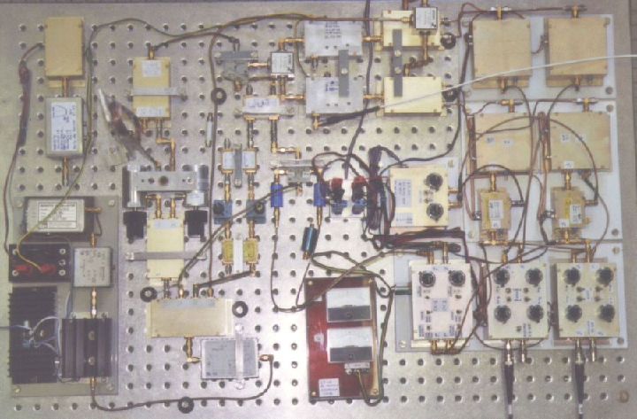
In search of the highest sensitivity at low frequencies, we decided not to use commercial hybrids or power splitters in the inner interferometer. In fact these devices are based on ferrite inductors and transformers, for they could flicker by modulating the carrier with the magnetic noise of the core; in addition, they could generate harmonics of the carrier frequency, noxious to the amplifier linearity. Conversely, the two couplers between the inner interferometer and the amplifiers can be of the ferrite type because they are crossed by a low residual power, or by the noise sidebands only. Thus we built two Wilkinson couplers, each with a pair of 75 PTFE-insulated cables and a 100 metal resistor. After trimming for best isolation at 100 MHz, the dissipative loss and the isolation turned out to be of 0.15 dB and 34 dB, respectively.
The phase of the inner interferometer can be adjusted by means of a set of semirigid cables and SMA transitions. In some experiments we also used a type of microwave line-stretcher consisting of coaxial pipes with locknuts, whose internal contacts are well protected against vibrations; the popular and easy-to-use U-shaped line stretcher adjusted by means of a micrometer is to be avoided. The attenuation can be adjusted with commercial 0.1 dB step attenuators. Two types were tested, manufactured by Weinschel (mod. 3035) and Texscan (mod. MA-508), with almost identical results. Measuring the ultimate noise of the instrument, we used only fixed attenuators and cables, manually trimmed. The instrument can still be used in this way for actual applications, provided the attenuator and the phase shifter be matched to the specific DUT.
The 100 MHz amplifiers consists of three cascaded modules in bipolar technology with low-Q LC filters in between. The first filter is a capacitive-coupled double resonator, while the second one is a LCL T-network. The use of two different topologies warrants a reasonable stopband attenuation at any frequency of interest because the stray pass frequencies do not coincide. For best linearity, we used for the second and for the third stage a type of amplifier that shows a third order intercept point of 35 dBm and a 1 dB compression power of 17 dBm, while the total output power never exceeds some dBm. The complete amplifier shows a gain dB and a noise figure dB.
The I-Q modulator and the I-Q detector are two equal devices built for this purpose (Fig. 3). The dissipative losses of the power splitter and of the 90∘ hybrid are of 0.5 and 1 dB respectively, while the SSB loss of the mixers is dB. A 10.7 MHz low pass filter is inserted at the IF port of each mixer to block the image frequency and the crosstalk. The quadrature adjustment, present in the earlier releases, is no longer useful because the quadrature error is compensated by the and matrices. The harmonics of the I-Q modulator must be checked; in our case none of them exceed dBm, which still insufficient for the amplifier to flicker. I-Qs of similar performances and smaller size, are available off-the-shelf at a lower cost. To duplicate the instrument this is the right choice; we opted for the realization of our own circuit for better insight, useful in the very first experiments. Finally, self interference from the mixer pump signal to the amplifier can be a serious problem, which caused some carefully designed layouts not to work properly.
The master source is a high stability 100 MHz quartz oscillator followed by a power amplifier and by a 7-poles LC filter that removes the harmonics. The output power is set to 21 dBm, some 8 dB below the 1 dB compression point. The source exhibits a frequency flicker of at Hz and a white phase noise of .
The preamplifiers at the detector output are a modified version of the “super low noise amplifier” [Pmi], consisting of three PNP matched differential pairs connected in parallel and followed by a low noise operational amplifier. The preamplifier, that shows a gain of 52 dB, is still not optimized22 2 A version of this amplifier optimized for 50 sources was studied afterwards [RLV04] for the input impedance of 50 . Terminating the input to 50 , the overall noise (preamplifier and termination) is of 1 (white), and 1.5 at 1 Hz (flicker plus white). The dc offset necessary to compensate for the the asymmetry of the detector diodes is added at the preamplifier output.
The matrices consist of four 10-turns high quality potentiometers, buffered at both input and output, and of two summing amplifiers in inverting configuration. The coefficients, whose sign is set by a switch for best accuracy around zero, can be set in the range.
The control consists of two separate integrators based on a FET operational amplifier in inverting configuration with a pure capacitance in the feedback path; the capacitors can be discharged manually. A dc offset can be added at the output of each integrator, which is necessary for the manual adjustment of the outer interferometer to be possible in open loop conditions. The loop time constant is of 5 s, hence the cutoff frequency is of 32 mHz.
Each circuit module is enclosed in a separate 4 mm thick aluminum box with 3 mm caps that provide mechanical stability and shielding. The boxes also filter the fluctuations of the environmental temperature. Microwave UT-141 semirigid cables (3.5 mm, PTFE-insulated) and SMA connectors are used in the whole radiofrequency section, while high quality coaxial cables and SMA connectors are used in the baseband circuits. All the parts of the instrument are screwed on a standard m2 breadboard with M6 holes on a 25 mm pitch grid, of the type commonly used for optics. The breadboard is rested on a 500 kg antivibration table that shows a cutoff frequency of 4 Hz. The circuit is power-supplied by car-type lead-acid batteries with a charger connected in parallel; in some cases the charger was removed.
Finally, we implemented a second prototype for the carrier frequency MHz. This instrument is a close copy of the 100 MHz one, and shares with it the readout system and the carrier control. Due to the long wavelength ( m), the Wilkinson couplers are impractical. Provisionally, we use a pair of 180∘ ferrite hybrids for the inner interferometer.
8 Adjustment and Calibration
For proper operation, the instrument first needs to be tuned and calibrated. The first step consists of compensating for the dc offset due to the diode asymmetry of the I-Q detectors, which is best done disconnecting the interferometer and terminating the input of the amplifiers to a 50 resistor. Secondly, have to set the readout system, as detailed in Section 4, which also include the measurement of the SSB gain. Thirdly, the control loop must be adjusted according to the procedure given in Section 5, and a suitable time constant must be chosen. This turns out to be easier if the inner interferometer is disconnected and the unused ports are terminated. Finally, the interferometer must be set for the highest carrier rejection.
The inner interferometer is first inspected alone with a network analyzer; as the the phase of the transfer function is not used, a spectrum analyzer with tracking oscillator is also suitable. Even at the first attempt, a slight notch, of at least a fraction of a dB, appears at some unpredictable frequency. Hence, the interferometer is tuned by iteratively ‘digging’ the notch and moving it to the desired frequency; acts on the carrier rejection, while acts on the frequency. The inner interferometer is then restored in the machine and the carrier rejection is refined by adjusting the fine carrier control and inspecting with a spectrum analyzer on the monitor output of the amplifier. A rejection of some 80–90 dB should be easily obtained. At this stage the machine is ready to use, and a carrier rejection of 110–120 dB should be obtained in normal operation.
8.1 Accuracy
Experience suggests that calibration difficulty resides almost entirely in the radiofrequency section, while the uncertainty of the instruments used to measure the low-frequency detected signals is a minor concern. In addition, the reference angles are only a second order problem because an error results in relative error in the measurement of and , which is negligible in most cases. The quadrature condition is even simpler because it is based on a null measurement at the output of the low-frequency section.
In order to understand calibration, one must remember that 1) and are voltage ratios, and 2) the instrument circuits are linear over a wide dynamic range. As a relevant consequence, the measurement of and relies upon the measurement of a radiofrequency power ratio instead of on absolute measurements. Actually, the phase-to-voltage gain (as well as the -to-voltage gain) is calculated as , which requires the measurement of . But the SSB gain is measured with the sideband method and Equation (18). Consequently,
| (32) |
A difficulty arises from the fact that must be a low power, dBm to dBm in our case, while can be higher than 10 dBm. Commercial power meters exhibit accuracy of some 0.1 dB, provided the input power be not less than some dBm; this is related to the large bandwidth (2–20 GHz) over which the equivalent input noise in integrated. Therefore, a reference attenuator is needed to compare to with a wattmeter. Actually, we use a synthesizer followed by a bandpass filter and by a 50 dB calibrated attenuator to generate the sideband, and we measure the sideband power at the filter output, before the attenuator; the filter is necessary to stop the synthesizer spurious signals. In our case MHz is in the frequency range of the two probes (HF-UHF and microwaves) of the available wattmeter, and we observed that in appropriate conditions the discrepancy never exceeds 0.05 dB; thus a value of 0.1 dB is a conservative estimate of the wattmeter uncertainty in the measurement of . Ascribing an uncertainty of 0.1 dB to the network analyzer with which the 50 dB attenuator is calibrated, the estimated accuracy of the instrument is of 0.2 dB.
9 Experimental Results
Our main interest is the sensitivity of the instrument, that is, the background noise measured in the absence of the DUT. Obviously, a great attention is spent on the low frequency part of the spectrum, where the multiple carrier suppression method is expected to improve the sensitivity.
In several occasions we have observed that the residual and are almost equal, as well as the residual noise spectrum of any combination in which . Rotating the detection frame with the matrix , the variation of the residual flicker can be of 1 dB peak or less. This means that the residual noise has no or little preference for any angle versus the carrier. Hence, after putting right the phase modulator method we did not spend much effort in calibrating the detection angle. Thus, the detected noise is the scalar projection of on two orthogonal axes that in most cases we let arbitrary. On the other hand, it would be misleading to give the results in terms of because the parametric noise is affected by the carrier power, and because the ratio is needed to determine and . Therefore, we give the results in terms of the normalized noise . Of course, becomes or if operates the appropriate rotation. The unit of is , hence , where implies that the unit of angle appears in the appropriate conditions. Anyway, the presence or absence of the unit has no effect on numerical values. As in real applications the measured quantities will be ‘true’ phase and amplitude noise, all the plots are labeled as and , given in and . Yet, in order to avoid any ambiguity, the radiofrequency spectrum is also reported (in dBm/Hz) and it is always specified whether or not the angle is calibrated.
Finally, the laboratory in which all the experiments are made is not climatized; a shielded chamber is not available, therefore the electromagnetic environment is relatively unclean. A 100 Mbit/s computer network is present, while the electromagnetic field of FM broadcastings in the 88–108 MHz band is of the order of 100 . Even worse, our equipment is located over the top of a clean room for Si technology where several dreadful (for us) machines are operated regularly, like vacuum pumps, an elecron microscope, etching and ion sputtering systems, etc., and we also share the power-line transformer with the clean room. No attempt has been made to hide stray signals by post-processing, consequently all the reported spectra are true hardware results.
9.1 Lowest-Noise Configuration
The first set of experiments is intended to assess the ultimate sensitivity of the instrument. Therefore the inner interferometer is balanced with semirigid coaxial cables only. In this conditions there results an asymmetry of a fraction of a degree in phase, and of several hundredth of dB in amplitude, which is corrected by inserting a parallel capacitance and a parallel resistance in the appropriate points, determined after some attempts. The actual correction is so small—some 0.5 pF and a few k in parallel to a 50 line—that the resulting impedance mismatch has no effect on the noise measurement accuracy. In the reported experiment the carrier rejection is of 88 dB in . While the automatic carrier control is operational, the fine control, no longer needed, is disconnected. With a DUT power dBm, the gain is .
9.1.1 Single-Arm Mode, for Real-Time Operation

Figure 7 shows the residual noise spectrum at the output 1 of the two radiofrequency channels and the cross spectrum. The detection direction, let arbitrary, is the same for the two channels. The white noise floor is dBm/Hz, which is 9 dB above the thermal energy dBm/Hz. This relatively high value is due to the high loss of the DUT-amplifier path, which is of 7.5 dB; this includes the 6 dB intrinsic loss of the couplers CP2 and CP4 and the insertion loss of CP3. The amplifier contributes with its noise figure dB. The noise floor corresponds to . Of course, if one radiofrequency channel is removed and the coupler in between (CP4) is bypassed, the gain increases by 3.5 dB while the white noise voltage at the output is still the same. Consequently the noise floor becomes .
On the left of Fig. 7, at Hz, the residual noise is of dBm/Hz (channel ) and dBm/Hz (channel ), which corresponds to a normalized noise of and . After correcting for the white noise contribution, the true flicker is of and of , for the two channels.

In a second experiment, the interferometer is removed, and the common input of the two radiofrequency channels (the input of CP4) is terminated. The automatic carrier control, still operational, compensates only for leakage. This experiment is intended to divide the noise of the amplifier and detector from that of the interferometer. Figure 8 shows the residual noise of the two arms of the same radiofrequency channel, accurately set in quadrature with one another. Obviously, only can be measured because there is no carrier to normalize to. Anyway, and are also reported for comparison, taking a fictive carrier power of the same value.
Comparing Fig. 8 to Fig. 7, the noise floor is unchanged, which means that the white noise of the interferometer is negligible. Without interferometer, is of dBm/Hz at Hz, which is some 1 dB lower than the previous value. This indicates that most of the flicker of Fig. 7 comes from the amplifier and detector, and that the interferometer noise is some 6–7 dB lower than that appears from Fig. 7, say /Hz at Hz.
9.1.2 Correlation and Averaging
Back to Fig. 7, the low-frequency correlation between the two channels is of dBm/Hz at Hz, hence . This is the stability of the interferometer, shared between the two channels. In fact, a noise reduction of dB would be expected if the two channels were independent, while the actual noise reduction is only of some 6.5 dB. In addition, this confirms the sensitivity inferred in Section 9.1.1, when we removed the interferometer. Smoothing the plot of Fig. 7, the correlated noise is lower than at a Fourier frequency as low as 3 Hz.

As explained in Section 6.1, the white noise floor, due to the resistive terminations and to the amplifiers, is expected to be rejected in the correlation between the two channels. Figure 9 reports the cross spectrum averaged over measurements, that is the maximum averaging capability of the available FFT analyzer. The observed noise reduction is close to the value of 24 dB, that is . Therefore, there is no evidence of correlated noise, and the sensitivity is expected to further increase increasing . In the reported conditions the background noise is at Hz, which is 15 dB lower than .

Figure 10 shows the residual noise spectrum measured with the two arms of a single radiofrequency channel carefully set in quadrature with one another, but still referred to an arbitrary detection direction. This simulates the detection of phase noise with the method. In the same conditions of the previous experiments the gain is of 77.8 , which is 3 dB lower. This is inherent in the detection scheme. As measurements spanning from 1 Hz take a long time, the experiment was stopped at , well before the cross spectrum could reach its final value, for dB. The residual noise is limited by for Hz, but not in the 1–10 Hz decade. Fitting this decade to the slope results in a correlated flicker noise is of some at Hz, which is the lowest value we have ever observed.
9.2 By-Step Attenuator Configuration

In an easier-to-use version of the instrument, we inserted a by-step attenuator (Weinschel, mod. 3055) and a microwave coaxial phase shifter in each arm of the inner interferometer, and we restored the fine carrier control. The phase shifters were set for the best carrier suppression, while one of the attenuator was set 0.1 dB off the optimum value, so that the carrier rejection of the inner interferometer was of 39 dB. This is slightly worse than the “true” worst case, in which a half-step attenuation error of 0.05 dB and a similar error of the phase shifter result in a carrier rejection of 42 dB. The residual flicker noise of the instrument, shown in the left part of Fig. 11, is of at Hz.
Then, we made two additional experiments. Firstly, we set the attenuators for the best carrier rejection, and we observed that the flicker noise does not change. This means that the 0.1 dB error of the attenuator is recovered by the fine carrier control without adding noise, and that the small signal delivered by the closed-loop carrier control does not impair low frequency sensitivity. Secondly, we checked upon the phase shifters with the methods of Section 9.1, and we observed a noise contribution negligible at that level. The relevant conclusion is that the flicker noise of Fig. 11 is due to the by-step attenuators. Assuming that the attenuators are equal, each one shows a flicker noise of at Hz. As only one attenuator is needed to measure an actual DUT, this is also the sensitivity of the instrument.
9.3 Simplified Configuration
A simplified version of the instrument is possible, in which the inner interferometer can be adjusted by step and the fine carrier control is absent. Of course, the dynamic range of the closed-loop control must be increased for the control to be able to recover a half-step error of the inner interferometer. This results in higher noise from the control and in additional difficulty to obtain a slow response. Actually, this configuration is the first one we experimented on.

The prototype makes use of two 180∘ hybrid couplers based on ferrite transformers in the inner interferometer, and has only one radiofrequency channel. Operating at dBm, the gain is of 80.1 . The direction of detection was calibrated carefully, therefore in this case the residual noise consists of true phase noise and of true amplitude noise. In order to simulate the worst case, we first trimmed the inner interferometer for a relatively deep minimum of the residual carrier, and then we set the attenuator 0.1 dB off that point. The residual noise spectra are shown in Fig. 12. The white noise is and . This is equal to the expected value , where dB accounts for the dissipative loss in the DUT-amplifier path and for the insertion loss of the 20 dB coupler; the noise figure of the amplifier is dB. The residual flicker is and , which is ascribed to the closed-loop carrier control.
10 Measurement Examples
The main conclusion of Section 9.2, that the flicker noise of a by-step atteuator is of at Hz, is a first example of measurement out of reach for other instruments.

As a second example of application, we measured a pair of 180∘ hybrid couplers (HH-109 Anzac, now Macom) with the scheme of Fig. 13 (top) inserted as the inner interferometer. The difference between the two samples turned out to be so small that a carrier rejection of 53 dB could be achieved by exploring the combinatorial permutations of the geometrical configuration. Hence, the background noise of the instrument was tested by replacing the hybrid pair with a 53 dB attenuator (Fig. 13 bottom). As the device noise detected on two orthogonal axes was almost the same, we did not calibrate the detection angle. Neglecting losses, the power crossing the two hybrids is the same because all the input power, 17.7 dBm in our case, reaches the 50 termination of the second hybrid. Although we did not use the correlation feature, we did not disconnect the unused channel. The result is shown in Fig 14. The noise of the pair is of at Hz, while the background noise is of . After subtracting the latter, the flicker noise of the pair is of , and therefore for each hybrid.

The same HH-109 hybrids, that are designed for the frequency range of 5–200 MHz, were tested at the input power of 14.9 dBm with the 5 MHz instrument. In this case we used only one radiofrequency channel, and we disconnected the other one bypassing the coupler in between (CP4); this results in a sensitivity enhancement of some 3.3 dB, that compensates for the reduced driving power. The measured noise is of at Hz, thus the flicker noise of the pair is of , corrected for the the instrument noise. Accordingly, the flicker noise of each hybrid is of at Hz.
The above results confirm the usefulness of the coaxial power dividers to obtain the highest sensitivity. As the hybrid is a transformer network, there are good reasons to ascribe the observed flickering to the ferrite core.
11 More about Stability and Residual Noise

Figure 15 shows a summary of the factors limiting the instrument sensitivity, most of which taken from Section 9. For comparison, the dotted lines report the residual noise of previous instruments: plot a is the double balanced mixer in average-favorable conditions, while plots b and c come from our previous works [RGG99, RG00a].
The limits of the radiofrequency electronics are taken from Section 9.1.1. Plot j refers to white noise, while plot f refers to flickering corrected for white. The correlation limit (plot k) is the white noise lowered by . The noise of the baseband electronics (plot l) is measured terminating the preamplifier input to 50 , and referring the output noise voltage to the DUT. Plots f, j, k and l (dashed lines) are related to levels independent of , for the corresponding and decrease as increases. A conventional power dBm is assumed.
Noise from the master oscillator (plot i) is measured with a phase modulator between the oscillator and the power amplifier, scaling the result down according to the actual oscillator noise. The modulation needed is of some 80–100 dB higher than the oscillator noise, for this only proves that the oscillator phase noise is negligible, without providing a precise result. Unfortunately, we have no information about the amplitude noise of the oscillator.
The “could-be mechanical stability” (plot h) is a reference value inferred from the residual flicker of dB at Hz that we measured measured at 9.1 GHz on our first interferometer [RGG99], under the obvious assumption that the mechanical fluctuations could not be worse than the overall noise we measured. We guess that the above result can be scaled down by 39 dB, which is the ratio (9.1 GHz)/(100 MHz), assuming a similar fluctuation in length. A phase fluctuation is equivalent to a length fluctuation , where m is the wavelength inside cables. Hence, the value of , taken as a conservative estimate of the interferometer flicker (Sections 9.1.1 and 9.1.2), is equivalent to . In the case of flicker noise, the appropriate formula to convert the PSD of the quantity into the Allan variance is , independent of the measurement time , as well known in the domain of time and frequency metrology [Rut78]. In our case the Allan deviation, that is the stability of the interferometer, is Å. The latter is far from the stability achieved by other scientific instruments, like the scanning microscope, for we believe that there is room for progress.
Acknowledgements.
Michele Elia, from the Politecnico di Torino, Italy, gave invaluable contributions to the theoretical comprehension of our experiments. Hermann Stoll, from the Max Planck Institute for Metallforschung, Stuttgart, taught us the trick of the detection. Giorgio Brida, from the IEN, Italy, shared his experience on radiofrequency. The technical staff of the LPMO helped us in the hardware construction.
References
- [AAC64] M. G. Arthur, C. M. Allred, and M. K. Cannon, A precision noise power comparator, IEEE Trans. Instrum. Meas. 13 (1964), 301–305.
- [All62] C. M. Allred, A precision noise spectral density comparator, J. Res. NBS 66C (1962), 323–330.
- [Aud80] Claude Audoin, Frequency metrology, Metrology and Fundamental Constants (A. Ferro Milone and P. Giacomo, eds.), North Holland, Amsterdam, 1980, pp. 169–222.
- [Cg94] Chronos group, Frequency measurement and control, Chapman and Hall, London, 1994.
- [CMLB97] S. Chang, A. G. Mann, A. N. Luiten, and D. G. Blair, Measurements of radiation pressure effect in cryogenic sapphire dielectric resonators, Phys. Rev. Lett. 79 (1997), no. 11, 2141–2144.
- [DR58] Wilbur D. Davenport, Jr and William L. Root, An introduction to random signals and noise, McGraw Hill, New York, 1958, (Reprinted by the IEEE Press, New York, 1987).
- [Fri44] H. T. Friis, Noise figure of radio receivers, Proc. IRE 32 (1944), 419–422.
- [GB75] J.-J. Gagnepain and R. Besson, Nonlinear effects in piezoelectric quartz crystals, Physical Acoustics (Warren P. Mason and R. N. Thurston, eds.), vol. XI, Academic Press, New York, 1975.
- [HJ85] Roger A. Horn and Charles R. Johnson, Matrix analysis, Cambridge University Press, 1985.
- [HJD52] R. Hanbury Brown, R. C. Jennison, and M. K. Das Gupta, Apparent angular sizes of discrete radio sources, Nature 170 (1952), no. 4338, 1061–1063.
- [Hor69] Charles H. Horn, A carrier suppression technique for measuring S/N and carrier/sideband ratios greater than 120 dB, Proc. Freq. Control Symp. (Fort Monmouth, NJ), May 6-8 1969, pp. 223–235.
- [ITW98] Eugene N. Ivanov, Michael E. Tobar, and Richard A. Woode, Application of interferometric signal processing to phase-noise reduction in microwave oscillators, IEEE Trans. Microw. Theory Tech. 46 (1998), no. 10, 1537–1545.
- [KB97] V. N. Kuleshov and T. I. Boldyreva, AM and PM noise in bipolar transistor amplifiers: Sources, ways of influence, techniques of reduction, Proc. Freq. Control Symp. (Orlando, CA), IEEE, New York, 1997, May 28–30, 1997, pp. 446–455.
- [Ken00] P. B. Kennington, High linearity RF amplifier design, Artech House, Norwood, MA, 2000.
- [Lab82] F. Labaar, New discriminator boosts phase noise testing, Microwaves 21 (1982), no. 3, 65–69.
- [Lee66] D. B. Leeson, A simple model of feed back oscillator noise spectrum, Proc. IEEE 54 (1966), 329–330.
- [LS73] William C. Lindsey and Marvin K. Simon, Telecommunication systems engineering, Prentice-Hall, Englewood Cliffs, NJ, 1973, (Reprinted by Dover Publications, 1991).
- [Mea83] M. L. Meade, Lock-in amplifiers: Principle and applications, IEE, London, 1983.
- [PG79] V. Petrovich and W. Gosling, Polar loop transmitter, Electron. Lett. 15 (1979), no. 10, 286–288.
- [Pmi] Analog Devices (formerly Precision Monolithics Inc.), Specification of the mat-03 low noise matched dual pnp transistor, Also available as mat03.pdf from the web site http://www.analog.com/.
- [RG00a] Enrico Rubiola and Vincent Giordano, Correlation-based phase noise measurements, Rev. Sci. Instrum. 71 (2000), no. 8, 3085–3091.
- [RG00b] , Dual carrier suppression interferometer for the measurement of phase noise, Electron. Lett. 36 (2000), no. 25, 2073–2075.
- [RG00c] , Improved correlation interferometer as a means to measure phase noise, Proc. 14th European Frequency and Time Forum (Torino, Italy), March 14–16, 2000, pp. 133–137.
- [RG01] , A low-flicker scheme for the real-time measurement of phase noise, Proc. 2001 Frequency Control Symposium (Seattle WA, USA), June 6–8, 2001, pp. 138–143.
- [RG02] , A low-flicker scheme for the real-time measurement of phase noise, IEEE Trans. Ultras. Ferroel. and Freq. Contr. 49 (2002), no. 4, 501–507.
- [RGG99] Enrico Rubiola, Vincent Giordano, and Jacques Groslambert, Very high frequency and microwave interferometric PM and AM noise measurements, Rev. Sci. Instrum. 70 (1999), no. 1, 220–225.
- [RLV04] Enrico Rubiola and Franck Lardet-Vieudrin, Low flicker-noise amplifier for 50 sources, Rev. Sci. Instrum. 75 (2004), no. 5, 1323–1326.
- [Rut78] Jacques Rutman, Characterization of phase and frequency instabilities in precision frequency sources: Fifteen years of progress, Proc. IEEE 66 (1978), no. 9, 1048–1075.
- [San68] K. H. Sann, The measurement of near-carrier noise in microwave amplifiers, IEEE Trans. Microw. Theory Tech. 9 (1968), 761–766.
- [Sho50] William Shockley, Electron and holes in semiconductors, Van Nostrand, New York, 1950.
- [Vit66] Andrew J. Viterbi, Principles of coherent communication, McGraw Hill, New York, 1966.
- [VSHK89] A. H. Verbruggen, H. Stoll, K. Heeck, and R. H. Koch, A novel technique for measuring resistance fluctuations independently of background noise, Applied Physics A 48 (1989), 233–236.
- [WFJ97] Fred L. Walls, Eva S. Ferre-Pikal, and S. R. Jefferts, Origin of PM and AM noise in bipolar junction transistor amplifiers, IEEE Trans. Ultras. Ferroel. and Freq. Contr. 44 (1997), no. 2, 326–334.
- [WGA+96] D. R. White, R. Galleano, A. Actis, H Brixy, M De Groot, J Dubbeldam, A. L. Reesink, F. Edler, H. Sakurai, R. L. Shepard, and Gallop J. C., The status of Johnson noise thermometry, Metrologia 33 (1996), 325–335.
- [Yok83] Yokogawa and Hewlett Packard (now Agilent Technologies), Tokyo, HP-4192A LF impedance analyzer; operation and service manual, December 1983.