M.S., Electrical and Computer Engineering
Master of Science
Electrical Engineering
Thesis
B.S., Mathematics and Physics, US Air Force Academy, 1997
M.S., Physics, Massachusetts Institute of Technology, 1999
Model And Fabrication Of A Proof-Of-Concept Polarimeter-In-A-Pixel
Abstract
I propose a new optoelectronic device that completely and instantaneously measures the incident light’s polarization for a narrow wavelength band in a single physical pixel. The device has four (or more) quantum-well active regions separated and topped by four (or more) linear gratings at different orientations. Electrical contact is made to each grating and to a bottom contact layer to measure four (or more) photocurrents. The device uses interference among many light paths to encode in four photocurrents four values that completely describe the polarization state of the incident light at a given wavelength. I begin with the motivation for the new device. Then, I report on two computational models: the first includes perfectly conducting gratings, and the second includes more realistic dielectric gratings. Next, I will describe the design and processing of a two-layer proof-of-concept device. Last, I will recount the trials of the first round of fabrication.
To my wife, Laura, for her love, support, tolerance and encouragement.
Acknowledgements.
I would like to thank Dave Cardimona at the Air Force Research Laboratory, Space Vehicles Directorate for his support and funding, and my advisor, Dr. Sanjay Krishna, for his support and advice. I owe a big thank-you to Peter Hill, Sunil Raghavan, Beth Fuchs, and John Zou for all their help with processing the sample. I need to thank Z. Liau at MIT Lincoln Laboratory for help with wafer fusion, and Kathy Sun and Sanh Luong at Zia Laser for help with lapping and polishing the device. I also would like to thank Paul Rotella Greg von Winckel, and Joe Evans Jr for their help designing, ordering, growing, and processing aspects of the demonstration polarimeter. For help with characterization of the various test devices, I need to thank Dang Le, Scott Gingrich, Ryan McGuire, and Beverly Klemme. Last, I would like to thank Dan Huang, Chris Morath, Paul Alsing, Tzveta Apostolova, Paul LeVan, Tom Caudill, Scott Tyo, J Piprek, Susumu Noda, Lutz Wendler and Shawn Lin for many hours of fun and helpful discussions. I appreciate Barrett Flake’s help with computing resources on several weekends. I also appreciate Michael O’Brien and Arezou Khoshakhlagh for their help with SEM and AFM images.The wave vector component in the direction perpendicular to the grating groove in the medium .
The component of the wave vector of mode . The real and imaginary parts of are always greater than or equal to zero.
Buffered oxide etch. A solution of buffered with .
Coefficients in layer that represent the field in that layer. The represents (fast, slow) or (TE, TM). The indicates the mode giving the x and y component of the wave vector. The indicates an up-going or down-going mode.
The transmission matrix relating the coefficients on one side of a slab interface to the other side of the interface.
Dynamical matrix. Used to find the transmission matrix.
A set of discrete symmetries enumerated by formed by translating the system by a displacement .
Degree of polarization.
The magnetic field parallel to the grating grooves vanishes.
The wave vector component in the direction parallel to the grating grooves.
The coordinate parallel the grooves of a linear grating.
A unit vector in the direction parallel to the grating groove.
The coordinate perpendicular to the grooves of a linear grating.
Inherent polarization uncertainty.
The matrix that expresses the conditions for boundary condition matching for modes inside the dielectric gratings.
Optical phase difference between two paths in the device.
Polarization response matrix: A matrix that relates the incident Stokes vector to the response vector.
Quantum-well infrared photoconductor.
Response vector: A vector containing the response or light absorbed by each quantum-well stack in the device.
The four stokes vectors.
The scattering matrix from the top reflective grating of the device.
The electric field parallel to the grating grooves vanishes.
The electric field has no z-component. Also known as ‘s’ polarization.
The magnetic field has no z-component. Also known as ‘p’ polarization.
The transfer matrix. Relates the fields at one end of a slab to the fields at the other extreme of the slab.
Chapter 0 Polarimetry background
1 Imaging polarimetry
An imaging polarimeter captures an image with both the intensity and some measure of the polarization state recorded for each pixel. A polarimetric image has more information than a simple intensity image and improves remote sensing and automatic target recognition [27]. Polarimetry can be used to identify materials and to distinguish samples from a cluttered background [31]. Polarimetry has also shown promise for mine detection [12]. On average, the pixels of polarimetric images of man-made objects have a higher degree of polarization (DOP) than the pixels of polarimetric images of natural objects. This pattern could be useful for spectro-polarimetric target detection with a target filling one pixel or less. Polarimetric data is often represented in terms of Stokes parameters.
The four Stokes parameters[6], which represent all the polarization information, are: , , , and where is the measured intensity of the light after passing through a linear filter at an orientation of degrees, and and are the measured intensities of the right or left circularly polarized fraction of the light.

The Stokes parameters have several useful properties. If you place the four parameters into a four-dimensional vector (called a Stokes vector), they form a linear vector space. This means that the Stokes vector of two beams of light added incoherently is the linear sum of the Stokes vector of each original beam. The is the intensity of the light and is always positive . The parameters will always satisfy the inequality . A useful way of representing the polarization is by a vector in a ball, called a Poincar sphere, shown in figure 1. The radius of the ball is the intensity of the light. Every polarization state is some vector inside the ball or on the surface of the ball. All points on the surface of the ball are pure polarization states. The degree of polarization (DOP), is the ratio of the radius of the polarization state vector to the radius of the ball. In terms of Stokes parameters, the DOP is given by . From the DOP and the above inequality, one can tell that , , and .
There are many approaches to imaging polarimetry instrument design. Some polarimeters only measure linear polarization and intensity (, , and ). Others will measure all four Stokes parameters. The choice of which combination of Stokes parameters to measure depends on the application. A full-Stokes-vector polarimeter will measure all four Stokes parameters at every pixel.
2 Other polarimeter designs
The current technology of imaging polarimeters cannot reliably measure high-spatio-temporal polarization or high-spectral-resolution polarization of a moving scene; the camera reports huge errors at the boundaries of objects in the scene or trades-off spatial and spectral resolution to achieve faster measurements.
The errors at the boundaries of scene-objects occur because a typical imaging polarimeter collects several different images of the same object, with the light emanating from the object passing through a different polarization filter in each image. The collected images are linearly combined with positive and negative weights to extract the polarization state at each pixel. To perform the subtraction, one registers pixels from the different images that represent the same point in the scene. However, because the images are taken at different times, any motion in the image will cause a registration error. Registration errors lead to subtracting two values that should be of the same object but are not of the same object. The difference will falsely report a polarization in the image with errors in the range of 100% [25].
U. S. Patent No. 5,045,701 by Goldstein and Chipman describes one such device. They use a rotating quarter-wave plate with a fixed linear filter. With a single focal plane, this device takes several images at different rotations, respectively, of the polarizing filter. Again, the collected images are linearly combined with positive and negative weights to extract the polarization state at each pixel. Again, one must register the pixels from the different images that represent the same point in the scene. As described before, any motion in the image will cause a registration error. This precludes the use of this apparatus to obtain polarimetric images of terrestrial objects from moving platforms, such as airplanes or orbiting satellites, or images of objects that are translating or rotating with respect to the apparatus.
Beekman and Van Anda used neighboring pixels to detect different polarizations; again the pixels are misregistered by one pixel width [4]. This approach uses quantum well infrared photodetectors with linear gratings. Quantum wells can only detect the component of light with the electric field perpendicular to the growth direction [16, 19]. With linear gratings, each pixel can only detect the component of the incident light with the electric field perpendicular the grooves of the grating. On a single focal plane, Beekman and Van Anda made neighboring pixels sensitive to vertical, horizontal or diagonal polarizations by using vertical, horizontal or diagonal gratings. Again, one linearly combines the neighboring pixels sensitive to the different polarizations with positive and negative weights. Because the pixels being combined image spatially neighboring points in the scene, sharp edges or bright points will register as erroneous polarization.
Another approach uses four separate cameras with a different polarization filter on each camera. The four cameras take simultaneous images of the same scene. Again, the appropriate images are linearly combined with positive and negative weights to extract the four Stokes parameters; however, parallax and camera misalignment will introduce registration errors into the derived image. Polarization error follows due to registration errors.
In a brand new type of spectral-polarimeter, pixel registration is achieved but spectral resolution is sacrificed [11]. In this case, the pixels reading nearby groups of spectral lines contain the polarization data. Due to this source of error, sharp spectral features will induce polarization errors. This example is called a polarimetric spectral intensity modulation spectropolarimeter, and is described in U. S. Patent No. 6,490,043 by Kebabian. This device measures the polarization of a single point in a scene by modulating the spectrum of the light with the polarization of the light and then measuring the spectrum of the light on a row of pixels. In order to find the polarization one must compare the modulated spectrum to the true spectrum. Because the true spectrum is not known, approximations must be made that necessarily sacrifice polarimetric and spectral accuracy and precision in favor of pixel registration. Their approach of encoding the polarization in the spectrum is very similar to approaches described at the Japanese SICE conference by Oka [23] and Locke [20]. Another polarimeter design that also records the polarization as a spatial pattern on the focal plane array is explained by Van Delden [9].
All current polarimeters are lacking in one of three areas. First is registration errors: the error is maximum at the boundaries of objects in a scene. The second difficulty is sacrificing spectral resolution: sharp spectral features still introduce errors. The third is a sacrifice in spatial resolution: one must trade-off the weight and volume of imaging optics, which normally limit resolution, with the weight and volume of beam splitters needed to divide the image onto several focal-plane arrays.
Chapter 1 Introduction to a polarimeter-in-a-pixel
The topic of this thesis is a device that should detect the full-polarization at each pixel, and at each frame, and at each wavelength. The device was first introduced in reference [29], and was also reported on in references [30, 7]. In this chapter, I describe the device.
1 Device description

In the device, shown in figure 1, quantum-well stacks are used in combination with linear gratings to determine the degree of polarization of incident light in terms of Stokes parameters. Interference from multiple reflections, diffractions and transmissions of the light propagating from and through the linear gratings modulates the absorption of the 1-diffracted orders at each quantum-well stack. The quantum-well stacks, do not absorb light having an electric field component in a plane parallel to the quantum well stacks [16, 19]. The non-absorbed propagating light is reflected, diffracted and transmitted at each grating as a function of its polarization. Interference translates the incident polarization into the amount of polarized light having an electric field with a component in the z-direction. This z-polarized component of the light is absorbed by the quantum wells.
Each quantum-well stack is included in a separate circuit having a voltage bias and a current meter. The voltage bias across each circuit is individually adjusted, and the photocurrent in each circuit, as measured by the respective current meter, is proportional to the flux of light absorbed by the respective quantum-well stack. The circuit diagram is similar to that of multi-color QWIP devices [10].
The four photocurrents are thus a measure of the polarization of the incident light by measuring what is ultimately absorbed by each of the four quantum well stacks. More particularly, the four currents are linearly mapped to the four Stokes parameters, which, in turn, represent the polarization of the incident light.
2 Principle of operation
To explain the principle underlying the polarization detection, consider a current-technology quantum-well photodetector including single quantum-well stack with a single linear grating and consider a simplified embodiment of the present invention with just two quantum-well stacks and two linear gratings. Using the single layer of gratings, this section will show the relevant physics of the quantum-well polarization selection rule for absorption, and the relevant physics of diffraction from a single grating. Using the two-layer structure, this section will show how the incident photons are split and then interfere to gain additional polarization sensitivity.
1 Single-layer device
(a) (b)
(b)
The quantum wells, and thus the quantum-well stacks, only absorb light with an electric field in the z-direction [16, 19]. Figures 2 (a) and (b) show two different polarizations of light propagating through a current-technology quantum-well infrared detector(QWIP). The QWIP is equipped with a linear grating in the x-direction (out of the page). This subsection will show that only the y-polarized light is absorbed.
Because the electric field is always perpendicular to the direction of travel, light propagating in the z-direction is never absorbed. Due to this property of light, and the polarization selection rule, the incident beam and the reflected beam are not absorbed – only the diffracted light has a chance of being absorbed.
Figure 2 (a) shows how the diffraction grating enables light to be absorbed by the quantum wells. The incident light is not absorbed on the first pass through the quantum well material. The reflected light is also not absorbed. The diffracted light has the electric field shifted into a component parallel to the z-axis. This light is absorbed.
A linear grating preserves the fast polarization (electric field parallel to the grating grooves) of light incident from the plane perpendicular to the grooves of the grating. Thus, the x-polarized light will be diffracted into x-polarized diffracted orders. As shown in figure 2 (b), the diffracted x-polarized light is still perpendicular to the z-axis and is not absorbed by the quantum-wells.
In this way, a simple QWIP with a linear grating can only detect the y-polarized component of the incident light. However, the single pixel just described will give the same response for a fixed intensity of 45-degree polarized light, 135-degree polarized light, right-circularly polarized light, left-circularly polarized light, and unpolarized light.
2 Two-layer test structure

To understand how my new device works, this section follows two paths of light through a simplified two-layer embodiment of the invention. To show an improvement over the old technology, I need to show how this new invention can distinguish 45-degree from 135-degree polarization in a single pixel.
The non-absorbed z-propagating light is reflected, diffracted and transmitted at each grating as a function of its polarization. One key element is that linear gratings also have polarization-dependent physics [26, 14]. Grating diffraction efficiency is different for fast polarization (no magnetic field parallel to the grating’s grooves) and slow polarization (no electric field parallel to the grating’s grooves).
For example, consider light with a 2.5 wavelength normally incident on a perfectly conducting grating with a 3 period, 1.5 grooves, and 0.75 depth. The fast polarization will be 14 reflected (into the 0th order) and 43 diffracted into the orders, and the slow-polarization will be 30 reflected (into 0th order) and 35 diffracted into the orders. In addition, polarized light incident on a linear grating will have a relative phase shift between the diffracted fast and slow polarization components [14].
In the case of a single grating, for a fixed intensity of light, we could distinguish x-polarized from y-polarized, but we could not distinguish 45-degree-polarized from 135-degree-polarized. I will now describe how interference from the second linear grating at an angle of 45 degrees will modulate the photocurrent measured across the quantum wells before the first grating.
Each incident photon is split at each grating and takes several paths through the device. Figure 3 shows an example of two paths that light can take that create polarization dependent interference and therefore lead to polarization dependent photocurrent. Recall, the actual device has four or more layers and many interfering paths. I will just trace through two simple paths.
For 45-degree-polarized incident light, the first path consists of a diffraction of light from the grating along the x-axis. I define that when the incident light reaches the first grating, the phase is 180 degrees. After diffraction, the component of the reflected +1 order that is polarized in the y-z plane has a phase of 105 degrees.
For 45-degree-polarized incident light, the second path consists of the transmission of the incident light through first grating. Transmission through this grating causes the light to become somewhat elliptically polarized with a major axis along the 45-degree orientation. The component of the light polarized in the y-z plane has a phase of -90º. The propagation of light from first grating to grating second grating advances the phase by 400 degrees. At the second grating, the light reflects backward, and the light component in the y-z plane now has a phase of 415 degrees. The magnitude and the phase shift in the light after reflection from a linear grating is highly dependent on the polarization of the light with respect to the grating. The light advances another 400 degrees in phase while propagating back towards the first grating. After the light forward diffracts from this first grating, the phase becomes 915 degrees, which is equivalent to 105 degrees + 90 degrees. We compare with 105 degrees because this was the phase of the light that took the first path, i.e. was diffracted and reflected to the +1 order.
Since the phases polarized in the y-z plane from these two paths do not cancel out, the quantum-well stack will absorb the light and generate a photocurrent. The absorption by quantum-well stack is proportional to the vector sum of the light from these two paths. The two paths have a phase difference of 90º, and therefore the two paths do not interfere constructively or destructively. This leads to a measurable amount of photocurrent across quantum well stack.
Next consider 135-degree polarized incident light. Again, I define that when the incident light reaches the first grating, the phase is 180 degrees. Since the light is normally incident, the quantum-well stack cannot absorb the light as it first enters the device . Again, interference exists between two possible paths that the photon can take. The interference is found by following a photon through two paths, which are in principle the same photon.
For 135-degree-polarized incident light, the first path consists of a diffraction from the first grating to the reflected and diffracted +1 order. The component of the diffracted light polarized in the y-z plane will have a phase of 105 degrees.
For 135-degree-polarized incident light, the second path consists of the transmission of the incident light through the first grating. After transmission through this first grating, the light is slightly elliptically polarized with a major axis along the 135-degree orientation. The component of the light polarized in the y-z plane has a phase of -90 degrees. The propagation of the light from the first grating up to the second grating advances the phase by 400 degrees. After reflection from the second grating, the light as a phase in the y-z plane of 505 degrees. This is the step that differentiates between incident light polarized along 45-degree and 135-degree axes. The reflection from the second grating gives a very different phase shift when the light is polarized with versus perpendicular to the grating grooves. Next, the light advances another 400 degrees in phase while propagating back towards the first grating. After the light forward diffracts from this first grating it is now in the same mode as the light that originally reflected and diffracted into the +1 order. The phase in the y-z plane is now 1005 degrees, which is equivalent to 105 degrees + 180 degrees.
The absorption by quantum-well stack is proportional to the vector sum of light from both paths. The two paths have a phase difference of 180 degrees, and therefore the two paths interfere destructively. This leads to a negligible amount of photocurrent across quantum-well stack. Therefore, the photocurrent across this first quantum-well stack changes for 45-degree polarized incident light compared to 135-degree polarized incident light.
In this example, I have traced through two paths from a two-layer device. To predict the actual photocurrents of the actual device, I would need to trace through thousands of paths in a structure with four or more layers. This process is done through a computer model described in the next chapter.
Chapter 2 Modeling the complete four-layer polarimeter-in-a-pixel
In order to validate the principle-of-operation described in the previous chapter, I developed a working electromagnetic model of the device using transfer-matrix techniques described in Andersson [1, 2] and Wendler [33]. The code was written in GNU C++ on windows-based computers and is available upon request.
Figures 1 and 2 show some results of this working electromagnetic model of the proposed device. On the graph’s ordinate, the fraction of incident light absorbed in the four quantum-well stacks respectively for 9.5 micron incident light. The abscissa of figure 1 shows the angle of linearly polarized incident light. The abscissa of figure 2 shows the phase lag between 0-degree polarized incident light and 90-degree polarized incident light. The phase lag smoothly changes the polarization from 45-degree linear to right circular to 135-degree linear to left circular. The graph demonstrates that the relative photocurrents from the four quantum-well stacks provide a means to measure the polarization of incident light.


1 The transfer-matrix method
The model that generated figures 1 and 2 is based on a transfer-matrix method. A transfer-matrix approach breaks the problem down into slabs. The modes in each slab are found separately. Boundary conditions at the interface between the slabs relate the electromagnetic state in one slab to the neighboring slabs. Each slab must be uniform along the z-axis. The slabs are designated by the index :
| (1) | |||||
| (3) | |||||
| (4) | |||||
| (5) |
where are the z positions of the interfaces between each slab.
The fields in each slab, (either an electric or magnetic field) are represented by a sum of coefficients multiplied by mode functions,
| (6) |
where are the coefficients and are the mode functions. The index represents the x, y component of the wave vector for that particular mode. Up-going modes are denoted () where , and down-going modes (-) where . The index indicates which of two states one is in for each wave vector. The two states could be TE and TM or fast and slow. For TE modes, the electric field has no z-component. For TM modes, the magnetic field has no z-component. For fast modes, the magnetic field parallel to the grating grooves vanishes. For slow modes, the electric field parallel to the grating grooves vanishes.
The field is chosen so that the 6 components of the electromagnetic field are implicitly stored in at most 2 components. For example, the electric field in the direction for TE modes and the magnetic field in the direction for TM modes. Given these two components and the wave vector for the particular mode, one can find all 6 components of the electric and magnetic vector fields.
The coefficients in each slab are collected into a vector that succinctly represents the fields in that slab.
Because the tangental fields are continuous across the boundary of each slab, we can easily find the coefficients that represent the field in slab if we know the coefficients in slab . The matrix that relates these two sets of coefficients is called a transmission matrix. The transmission matrix converts the coefficients in slab at to the coefficients in slab at :
| (7) |
Within a slab , one can also relate the fields at to the fields at by a diagonal propagation matrix,
| (8) |
where and both the real and imaginary parts of are taken to be positive.
Using the same parameters as reference [2], the quantum wells were represented with a Drude model where was imaginary and represented absorption.
By stringing together the transmission matrices and the propagation matrices, we can relate the fields at one extreme of the stack to the fields at the other end of the stack through the transfer matrix :
| (9) |
To use the transfer matrix, we need to know boundary conditions at one or both ends of the stack. In our case, the incident light is given. Therefore we know the coefficients of the up-going modes in layer . This forms one boundary condition. Also, the top grating is completely reflecting so the upward and downward traveling light at layer are related via a scattering matrix,
| (10) |
If I break up the transfer matrix T(1,N) into four matrices relating the up-going and down-going coefficients,
| (11) |
where the indexes are suppressed, then, by using the boundary conditions, I find the fields at layer , in terms of the incident coefficients are given by
| (12) |
Using the scattering matrix in equation 10, I find the down-going modes at layer from the up-going modes. Using the transfer matrix, these modes can be propagated to any layer in the structure.
The transfer matrix takes into account infinite reflections and interference. This is the main advantage of the method. However, the solutions of thick structures, where , involve inverses that become unstable. Therefore, the transfer-matrix method degrades as the structure being modeled becomes thicker and higher order modes are considered.
2 Transmission matrices for the quantum-well slabs
The first type of transmission matrix we need is for the quantum-well slabs. The interface is assumed smooth so the modes are not mixed; we need only consider reflections and transmissions. The transmission matrix is given by
| (13) |
where and are the Fresnel reflection and transmission cofficients respectively and is an index which indicates if we want the TE or TM case.
In the case of anisotropic media, the Fresnel coefficients need to be more carefully defined. The coefficients are normally defined in terms of a plane wave with the electric field perpendicular to the plane of incidence (TE), or a plane wave with the electric field parallel to the plane of incidence (TM). Also, the traditional definition of the angle of incidence and angle of transmission is insufficient in uniaxial media because the dispersion relation relating , , and is different for and polarization.
To clarify, I present the dispersion relation for a uniaxial non-istropic material in terms of the wave vector components. The dielectric constant is the same for the and directions, denoted and different for the direction, denoted . Due to the continuous translational symmetry parallel to the flat interfaces of the layers, the vector is preserved across the interfaces. For polarization we have
| (14) |
and for polarization we have
| (15) |
For future convenience, the real part of the electric field for TE modes is in the direction . The real part of the magnetic field for TM modes is in the direction .
The Fresenel reflection coefficient for polarization from layer to layer is,
| (16) |
and the transmission coefficient,
| (17) |
where is the wave vector in the medium of the th layer, likewise and are the magnetic susceptibilities of the incident and transmitted material respectively, and is the normal vector to the surface which in our case is always .
For polarization, the transmission and reflection coefficients are
| (18) |
and
| (19) |
3 Modes in the bulk structure
I am solving a problem involving gratings. A tutorial introduction to the methods of solving diffraction grating problems is given by Petit in Ref. [26]. Grating periodicity places limits on the modes that I can consider in the bulk. I approximate the periodic grating to have an infinite extent. For electromagnetic waves of frequency in the presence of a linear grating, the fields must satisfies the quasi periodicity condition,
| (20) |
where is the component of the incident wave vector perpendicular to the grooves of the grating. The fields can then be expressed as a sum of a discrete set of modes,
| (21) |
where are unknown complex constants that span the solution space and are determined by matching the boundary conditions,
| (22) |
| (23) |
| (24) |
and where is the index of refraction of the material and . When , I take to be the positive imaginary root. The terms with are referred to as evanescent modes. Terms with are called propagating modes.

This is the case for a one-dimensional grating. The two-dimensional generalization involves finding a separate for each discrete symmetry where and enumerates the discrete symmetries. The are called reciprical lattice vectors, and they satisfy the equation
| (25) |
where is a Kronecker delta. The reciprical lattice vectors are given by where is a unit vector parallel to the grating grooves and is the two component normalized antisymmetric tensor and . Because each discrete symmetry is a two-dimensional vector, we cannot find a set of reciprical lattice vectors if there are more than two independent discrete symmetries. Physically, more than two independent discrete symmetries will lead to an infinitely dense set of modes to consider.
In my structure, I need to have four or more gratings at four or more different orientations. However, if they are independent discrete symmetries, I will have an infinite number of modes to consider. To solve this problem, I constrain the discrete symmetries to be linearly dependent. I limit my attention to cases where the period and orientation of the four gratings form a repeating unit cell as shown in fig. 3. Each grating has one reciprocal lattice vector. Because our four gratings share a repeating unit cell, the reciprocal lattice vectors and are formed by .
With this, I have a description of the modes in the bulk and a method to propagate them using a transfer matrix.
4 Modes in a Perfectly Conducting Grating
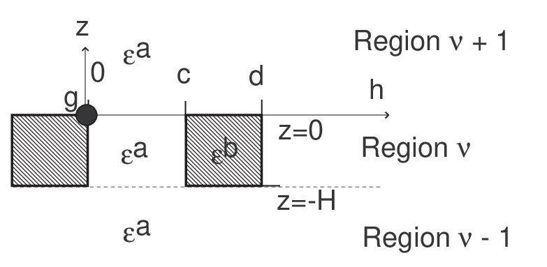
The modes in a perfectly conducting, metal grating are particularly simple. Because each grating is at a different angle, I choose two new variables for the coordinates parallel to the grating groove, , and perpendicular to the grating grooves, . Figure 4 is a diagram of the coordinate system. The gratings are perfectly conducting for . For a grating with grooves along the g-direction, the fast modes are
| (26) |
and the slow modes are given by
| (27) |
5 Modes in a Dielectric Grating
The modes for a dielectric grating are considerably more complex. I found the modes are a mixture of fast and slow modes, and the fields are represented by the waveguide modes:
| (28) | |||||
| (29) | |||||
| (30) | |||||
| (31) |
To slightly simplify the expressions in this section, I have dropped the superscript indicating which layer is being referenced.
To solve the boundary conditions at the interfaces of constant value, the modes inside the grating must be a specific superposition of fast and slow components. The next several paragraphs describe how to find the superposition of fast and slow modes that satisfies the boundary conditions at and .
The solutions in each region are expressed as
| (32) | |||
| (33) | |||
| (34) | |||
| (35) |
where
| (36) | |||||
| (37) |
and where is or for fast or slow mode. For all the dependencies inside the grating layer, the coordinate spans the range, . I also have the constraint
| (38) |
such that for both regions with dielectric constant and , the -momentum for a particular fast or slow mode is
| (39) |
where .
By matching boundary conditions at and , I found the following system of equations:
| (40) |
where this equation satisfies
| (41) |
where
| (42) | |||
| (43) | |||
| (44) | |||
| (45) | |||
| (46) | |||
| (47) | |||
| (48) | |||
| (49) | |||
| (50) |
and where is an offset momentum in the direction set by the incident light. To find the modes, we make and both functions of , and we scan until we find values where . Each of these values is a mode of the grating and enumerated with the subscript . For , all will be either purely real or purely imaginary.
For , the matrix becomes block diagonal. Due to symmetry considerations, the location of the zeros of are independent of . Therefore, for compuational simplicity, I found separately scanning the determinant of each submatrix was faster and more reliable than finding the zeros of the entire matrix in one scan.
For each zero we have one vector that spans the null space that satisfy eq. (41). I have found that in only two cases is the null space multi-dimensional, and in both cases the associated mode is trivial( and ) and should be omitted. These null vectors can be found using the singular value decomposition.
Finding the zeros was a major hurdle in the process. Many curves are like parabolas that reach down and barely cross zero. These situations need to return the two zeros or the resulting transfer matrix is singular.
6 Matching boundary conditions at slab interfaces
Matching boundary conditions at each interface is accomplished with the following steps: Set up the boundary requirement in terms of the the fields , and the appropriate map (eqns. 28 - 31) from to the vector fields of interest. Multiply both sides of the equation by a list of complementary modes and integrating over a unit cell. For example, the complimentary mode to is . Perform this with enough complimentary modes to form a square non-singular matrix. The expression will take the form of
| (51) |
where the matricies are known as the dynamical matricies. This expression can be used to solve for the transmission matrix,
| (52) |
A few final notes. The modes in the grating need not be orthogonal because they do not satisfy the Sturm Louiville conditions. I do not present the integrals here because I performed them numerically in the C++ code. Currently, the pixel-polarimeter model has about 20 design parameters and 20 parameters to describe the physics of the constituent materials and the incident light.
7 Calibration and Measurement Uncertainty
Using this toolbox, the C++ code starts from a given incident polarization state, calculates the coefficients at layer , propagates these coefficients to the regions above and below each quantum-well stack, and calculates the energy lost in each of the quantum-well stacks. The absorption by the quantum-well stack is proportional to the energy lost across the stack. The photocurrent is proportional to the absorption. In this way, I can predict the photocurrent from any number of layers given a pure, incident polarization state. The photocurrents representative of unpolarized light are found by averaging the photocurrents from x-polarized light and y-polarized light.
Because the Stokes vectors are a linear vector space, the response of an arbitrary incident polarization state can be summarized in a polarization response matrix (). This matrix maps the four components of the incident light’s Stokes vector to the photocurrents :
| (53) |
where the index runs from 1 to the number of readouts . For full polarimetric detection is required.
If ,the represents an over-determined system. The pseudoinverse, i.e. least squares fit, gives the Stokes vector from the device readouts11 1 I am grateful to Paul Alsing for reminding me about the pseudoinverse in over-determined systems.. The Stokes vector in matrix notation with the pseudoinverse is given by,
| (54) |
where is the transpose of the matrix . I will abbreviate the pseudoinverse of the matrix as
| (55) |
From the error propagation formula, the device’s ability to distinguish the distinct Stokes vectors is found to be
| (56) |
where is the uncertainty in the Stokes vector and is the uncertainty in the readout. If the uncertainty in the different readouts is equal, the device’s inherent polarization uncertainty factor is given by
| (57) |

Conceptually, the uncertainty in can be understood as the ability to distinguish two Stokes basis vectors () on a two-dimensional readout vector space. If the uncertainties in the two dimensions of the readout space are assumed to be equal, , then the inverse can be calculated analytically and gives the uncertainty to be
| (58) |
where is the angle between the Stokes basis vectors and is the length of the Stokes basis vector as depicted in fig. 5. The uncertainty in each Stokes vector is found to be inversely proportional to the magnitude of that Stokes basis vector and to the sine of the angle between that Stokes basis vector and the other three Stokes basis vectors.
In order to relate the inherent polarization uncertainty factor to a meaningful polarization detection performance, I need to know the signal to noise ratio of our quantum-well detectors. Using current QWIP cameras as a reference [24], each quantum-well readout can detect changes in photocurrent larger than about of a room-temperature signal (this corresponds to an of for a blackbody background). This gives us a signal-to-noise ratio for the photocurrent from each quantum-well stack.
Using these figures, the normalized Stokes error is given by
| (59) |
A typical signal of interest in the infrared is 2% to 5% linearly polarized. This means that for a signal to noise ratio of 2, we need .
To simplify the data presentation, unless otherwise specified, the subsequent plots will show the device’s worst case polarization uncertainty factor
| (60) |
8 Results
I constructed a C++ code from these elements to model the behavior of the proposed device. In this section, I will relate some of the results of the model indicating the underlying physics and ways to improve performance.
1 Using Perfectly Conducting Gratings
The predicted response of a pixel-polarimeter at is shown in figs. 1 and 2. In both plots, the pixel-polarimeter that is modeled has quantum wells each with peak absorption at , well width of and barrier width of . The quantum well absorption was modeled with a Drude model, and the Drude model parameters we used were taken from Anderson and Lundqvist’s paper [1]. The gratings are structured with orientations as shown in fig. 1. The gratings at and have periods of , and, due to the unit cell, the gratings at and have periods of . I refer to the period of the gratings at and as the base period. All gratings have depths of , and duty cycles with GaAs for of each period followed by a perfect conductor for of the period. The contact layers above and below the gratings are each.
Fig. 1 shows the linear-polarization responses of the four layers of the pixel polarimeter. The relative response changes as the angle of the linearly-polarized incident light varies. Fig. 2 shows the elliptical-polarization response of the four layers of the pixel polarimeter. The relative response changes as we change the phase lag between an -polarized and a -polarized plane wave. Notice that at phase lags of and the waves are linearly polarized with angles of and respectively.
To keep these scans representative of the scattering physics and independent of the quantum-well design choices, we set the quantum-well peak-absorption wavelength equal to the wavelength of the incident light.


In figs. 6, 7, and 8, we show the regions of parameter space with reasonable polarization detection performance. The dark regions correspond to parameters for a given incident wavelength where . In these regions for some reasonable QWIP noise and performance values, the device can detect changes of .
Fig. 6 shows how the polarization detection sensitivity changes as I vary the wavelength and the base period of the four gratings. The responses from the four layers shown in figs. 1 and 2 correspond to the parameters of the upper-left dark region of fig. 6.
The angled, dark streaks in figure 6 near 11 microns show a pattern that can be exploited in designing a push-broom imaging spectral polarimeter. As one moves along the focal plane of an imaging spectral polarimeter, the pixels detect different wavelengths. If the focal plane is designed with a period that gets larger as the wavelength gets larger, the resulting structure will allow near uniform polarization sensitivity across a region of the spectrum.
Fig. 7 shows how the polarization detection sensitivity changes as I vary the wavelength and the width of the dielectric grooves in all four gratings. In fig. 7 the computer simulation becomes unstable for small groove widths and large wavelengths. Under these circumstances, not enough light penetrates through to the deepest MQW stack to maintain a transfer matrix that can be meaningfully inverted.
Fig. 8 shows how the polarization detection sensitivity changes as I vary the wavelength and the thickness of the contact layers above and below each MQW stack. The device’s dependence on interference between the grating layers can be inferred from fig. 8. As you vary the contact layer thickness by you change the distance between the gratings by and the round-trip path-length difference by where is a positive integer representing interference from layer . The constructive or destructive interference is caused by two paths for light with an optical phase difference that changes with and in the following manner:
| (61) |
where is an integer. The constructive or destructive interference can be maintained if we change the contact layer thickness and the wavelength in such a way that is held constant. For constructive interference features, is even. For destructive interference features, is odd. In order to detect the polarization, interference is needed from some round trips between gratings at different orientations. Full polarization detection requires interference from all four gratings.
We can compare the slope of the trends on fig. 8 to Eq. (61) by solving for :
| (62) |
In our code, . For interference between the first and fourth grating, . For contact layer thickness around the distance between gratings is about . Recall the grating depth is . This means the actual distance traversed across the four gratings is nearly . Because the wavelength of 10 radiation in GaAs is about , the phase must advance about during the round trip across the four gratings. From the distance traversed, we determine the choices of to be for constructive interference and or for destructive interference. A choice of and gives a slope of . The slope of the thin line near and a contact thickness of is . This analysis can be repeated for the other clearly defined lines in fig. 8 to discover which interference paths dominate the polarization detection for the various wavelengths and contact layer thicknesses.
2 Using Dielectric Gratings
The polarization sensitivity can be further improved by increasing the fraction of light reaching the quantum wells deep inside the pixel. Again, to keep the scans representative of the scattering physics and independent of the quantum-well design choices, as we change wavelengths, we set the quantum-well peak-absorption wavelength equal to the wavelength of the incident light.

In fig. 9, we plot the worst case polarization uncertainty factor for a sample set of design parameters as a function of wavelength. Although not universal, the dielectric grating device does have a generally lower uncertainty than the perfectly conducting grating counterpart. For this particular scan, the gratings periods were the same as the scans from figs. 1 and 2. The dielectric grating was formed by rectangular strips of air.
The reason for the improved performance for a dielectric grating design is that more light is able to propagate through the -layers of the pixel leading to a stronger signal. In the case of perfectly conducting gratings, the stronger reflectivity causes a very small fraction of the light to reach the deepest quantum wells.
9 Future modeling work
There are many improvements that can be done with the model. First, the code is still very unstable. I cannot model structures with 5 or more layers because the transfer matrices become singular. One way to avoid this problem is to re-write the code with a scattering matrix approach. Another possibility is to use a finite time domain (FTD) model. Although the structure is tall, the unit cell is small and the solution should be possible in a resonable amount of time. This FTD approach will be too slow for extended scans of the parameter space, but it could confirm the presented results.
The current code has several improvements possible. The code currently assumes a real dielectric constant in the grating. In practice, the GaAs is n-doped and will have some free carrier absorption. Incorporating a complex dielectric constant for the grating would allow us to model these effects. The modes used for all the calculations in this section were the set of modes shown in figure 3. I suspect the stability would be improved if I used all modes that lie within a given radius. Last, the process of finding the zeros of can be improved dramatically. Currently, I sample the curve at a fine interval and search for when the function changes sign. I should be scanning for the extrema of the curve and using these to bound the search region when finding zeros.
With whatever code one chooses, there are also many tasks left to be solved. If a focal-plane array for a grating spectrometer were to be constructed, the depth of each grating would need to remain fixed across the focal plane. However, something must be varied so that the pixels will be optimized for the wavelength of the incident light falling on that pixel. Figure 6 suggests the period could be a good choice to vary.
Also, can the device be used in conjunction with a Fourier transform imager? Would one need to know the as a function of wavelength for each pixel? Will this perform better than the grating spectrometer?
Last, one can always further scan or explore the 20-dimensional parameter space to find large islands of strong polarization sensitivity or parameters that are more easy to fabricate. I am particularly interested in using layers, rather than the demonstrated . This will introduce an over determined system and average out noise. A modeling study of this approach would be valuable.
Chapter 3 Process design for a two-layer polarimeter-in-a-pixel
The next formidable challenge was to find a process that will allow fabrication of the device. We begin with a proof-of-concept two-layer test structure. The purpose of this structure is to demonstrate the underlying physics of the proposed device, and to pave the path for fabricating the more complex four-layer structure.
The final semiconductor structure is similar to the photonic crystal structures built by Lin, Flemming, Yamamoto, Noda, [18, 35, 3]. Lin and Flemming used Si and a pattern of etchings, regrowth, and chemical-mechanical-polishing. Aoki used InP and micromanipulation move individual trays of periodic gratings onto a stack. Yamamoto and Noda used GaAs and a pattern of etching gratings on separate wafers, wafer-to-wafer bonding, and etching away the substrate.
The regrowth option is difficult when one needs to grow quantum wells over a grating[34]. Re-achieving planarization is even more challenging, and the resulting quantum wells are of low quality which degrades their responsivity and the intersubband selection-rule critical for our application. The micromanipulation technique is useful for fabricating gratings, but the technique is foreign to detector development, and is not in wide spread use even among research organizations.
I anticipate that a wafer fusion approach will be more successful for building the pixel-polarimeter. The quantum wells will each be grown on a perfect substrate and then gratings will be etched and finally joined. The technique has been demonstrated on GaAs, a favored material system for quantum-well devices and was first developed by Dr Liau’s group at MIT Lincoln Laboratory, an Air Force FFRDC (Fedrally Funded Research and Development Center) [17].
Because the test structure only has two layers, these pixels cannot detect the full polarization state. The full polarization state requires four parameters. With a two-layer structure we can measure at most two parameters per pixel. This means that given two of the Stokes parameters, we should be able to measure the remaining two.
In this chapter, I review the techniques on which I based my process for the device fabrication. I will discuss the wafer fusion in more detail, substrate removal, and the design of the mask set.
1 Process overview
The process I designed uses wafer fusion to bury quantum wells between two gratings. We begin with a standard wafer with a thin (300 Angstrom) AlAs etch stop layer, an n-doped contact layer, 50 repetitions of a quantum-well followed by a barrier, and topped off with a second n-doped contact layer. We cleave the wafer into smaller pieces. On both pieces, we grow to protect the surface. On the first piece, we etch gratings. On the second piece, we do not etch gratings. We then wafer fuse the epilayers of the first piece and the second piece together. Next, the substrate of the second piece is removed by a selective wet chemical etch. The sacrificial etch stop layer is also removed. Now, gratings are etched into the stacked epilayers. We now have two quantum-well stacks and two gratings stacked atop one another. After the top grating, we deposit the n-metal for the top contact.
Now we isolate pixels. We etch the top mesa, and then with a slightly larger mask, we etch the bottom mesa. In order to make contact to the middle mesa, we need to run a contact pad from the bottom of the tall pixel up a wall to the middle layer of the tall pixel. We also need to insulate this middle contact pad from the n-doped bottom surface. To insulate the middle contact pad from the bottom surface, we deposit a layer of . The coats all walls and surfaces of the structure. Holes need to be opened in the to allow contact to the top of the pixels, middle, and bottom of the pixel. In order to ensure electrical contact across the interface, I make separate contact to a layer right above and right below the fused interface.

2 Wafer fusion overview
Wafer fusion and wafer bonding are techniques used to join two materials. Typically, but not always, wafer bonding refers to the use of an adhesive or intermediate layer, and wafer fusion refers to direct union of the two materials without an adhesive [21]. Wafer bonding is an older technique and will be skipped in this report. In addition to direct fusion and bonding with an adhesive or intermediate layer, anodic bonding is a third category of wafer fusion that makes use of an electric field to encourage the bonding process [28].
In 1986, Lasky first reported wafer fusion to achieve a high quality Si crystal over an insulator [15]. In 1990, Liau and Mull from MIT Lincoln Laboratories first reported wafer fusion in III-V semiconductors [17]. They reported bonding n-doped and p-doped materials and demonstrating normal diode characteristics. Liau and Mull also reported success on joining materials of different lattice constants. All their wafer fusion was done on samples with fused areas smaller than . Since these seminal papers, many people have achieved wafer fusion with GaAs, InP, and Si surfaces; these examples and studies will be addressed in the body of this chapter.
Wafer fusion is accomplished by first cleaning and polishing each sample, placing and aligning the two wafers together in an environment, and then applying heat and pressure to allow the bonds to break and reform across the interface.
The wafer surfaces to be fused need to be smooth and clean to enable wafer fusion to take place. The surfaces can to have a local RMS roughness of no greater than about 10 Angstroms, and the overall wafer surface must have bowing of less than 5 per 4 wafer [28].
In some cases, one of the layers can be prepared with shallow channels to allow liquid and gas bubbles to escape and improve the uniformity of the fused surface [21]. Another alternative is to include gratings or other patterns that allow bubbles to percolate to these collection points [17].
After the wafers are cleaned and joined, they are heated under pressure. The device that performs this process is called a wafer fusion reactor.
The original paper by Liau et.al. on wafer fusion, used a wafer-fusion reactor based on the differing coefficients of thermal expansion between graphite and quartz [17]. A similar setup was used by ref. [36]. Others have found the pressure required is not that large; conventional pressure source can also work. The setup used at University of California, Santa Barbara (UCSB) is based on a half dome pressing the two wafers together. The pressure source is tightening screws that hold the dome in place. The dome is critical because it diminishes the dependence on tightening the screws evenly [21].
Wafer fusion is facilitated by heat and uniform pressure. The pressure brings the two surfaces into contact and eliminates air bubbles [28]. The heat allows the crystal bonds to re-arrange and join the two surfaces. The wafer fusion reactor is designed such that the two wafers experience nearly uniform pressure. The pressure used in wafer fusion varies from 3 kPa to 3 MPa [5]. Higher pressure should allow fusion at lower temperatures.
3 Substrate Removal Overview
One of the dominant reasons to use wafer fusion is to transfer the epitaxial layer of one wafer onto the epitaxial layer of the second wafer. Once wafer fusion has been performed, the substrate of one of the wafers needs to be removed [36, 21]. This is facilitated by the use of a pregrown, thin, etch-stop layer on the substrate to be removed.
One problem not clarified in the literature is how to protect the back side. One method that we considered was to spin photoresist on the back. Another possibility is to mount the samples on a Si wafer or a glass slide with wax. As will be discussed in the next chapter, the glass slide technique was found to be better.
To remove GaAs substrates, Zhu suggests jet etching with - solution with a PH of 8.4. During jet etching, protect the wafer edges with wax to prevent undercut. The etching will stop at any layer with () or a lattice matched InGaP layer. Both InGaP and AlGaAs etch stop layers can be removed with HCl.
The GaAs vs AlAs selective etching technique which was best documented was a citric acid : etch [32, 13, 8]. Citric-acid monohydride is mixed 1:1 with deionized water to form a citric-acid solution. The citric-acid solution is then mixed with at a ratio of 4:1 to form the etching solution. The solution has a selectivity for etching GaAs over AlAs of over 1000 to 1.
As explained in the next chapter, we deduced a few missing details not mentioned in the literature. The etch rate was not sufficiently uniform to remove the entire 500 micron substrate with just the wet etch, so we needed to lap the substrate down to 100 microns. We also found the solution looses potency after a couple of hours so the solution needed to be replaced several times during an etching procedure. The end-point is easy to tell because the rough surface of the etched GaAs becomes a smooth glass like surface when the etching reaches the AlAs. Last the etch-stop layer should not be too thick because the AlAs forms a stressed oxide when exposed to the solution [8]. The stressed oxide will crumble thin samples.
4 A map of the mask set
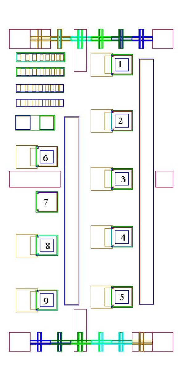
With these processes in mind, I designed the mask set using AutoCAD software.
Each die contains six pixels optimized to distinguish between two Stokes parameters given the other two Stokes parameters are known. Each die also contains a number of diagnostic structures. The die is shown in figure 2.

Each two-layer pixel on the die allows us to make contact to the top, middle, and bottom of the pixel with separate wire bonds. Figure 3 shows an SEM of the contact pads to the three layers of the pixel from our first round of fabrication. On top of each pixel, we have a top contact pad. The ‘C’ shaped structure to the left of the pixels is the middle layer’s contact pad. The middle contact pad has metal arms that climb up to the mesa and make contact with the middle of the structure. The long strips to the right of the column of pixels form a bottom contact pad. Each contact pad is about 200 to 250 microns. The large size was to enable easy wire bonding.
The right column contains pixels 1 through 5 which are each designed to be sensitive to distinguish two polarization states. Pixel 8 on the left column is also designed to distinguish polarization states. Table 1 lists the design parameters of these six pixels and their intended polarization sensitivity. The next section explains how I chose these design parameters and how sensitive the performance is to variations in construction.
In practice, the fabrication process will probably not be able to guarantee the design parameters to allow predictive design of the structure. I expect that the irregularities in the manufacture process will primarily shift the optimal wavelength for the polarization sensitivity.
The left column contains mostly diagnostic devices. The top four horizontal bars are mesas with small contact pads at varying distances from each other. I will refer to these as ohmic contact probing mesas. There is one such horizontal mesa for each depth that ohmic contacts are to form. These structures will allow us to measure the quality of the ohmic contacts.
Below the ohmic contact probing mesas, two small squares side by side will test the electrical behavior of the fused interface. The left square is just below the fused interface; the right square will be just above the fused interface. Measuring the resistance across these two pads will give some indication of the resistance across the fused interface.
Pixels 6 and 7 are to test the quantum wells. If we have difficulty with the main experiment (pixels 1-5 and 8), these two structures will allow us to test if the quantum wells in either layer are working, and if so which layer is providing the photocurrent. This could also be a useful way of measuring the amount of free-carrier absorption in the doped region between the two quantum-well stacks. Pixel 6 has no gratings at the fused interface, and a grating at the very top of the structure. Photocurrent can be generated and measured across both sets of quantum-well stacks. Pixel 7 has had the top quantum-well stack etched away and consists only of the lower quantum-well stack and a grating on the same layer as the fused interface.
Pixel 9 is a copy of pixel 4 with one change. The gratings extend to the edge of the mesa. There was no clear answer or reason that the gratings should be exposed to the air or trapped in the semiconductor structure. This device explored this variation. I also hoped this device would expose the fused gratings to facilitate good SEM pictures.
Last, there are several large rectangles on the edge of the die. These are windows to facilitate aligning the metal-field masks. They were also intended as visible alignment marks to be used in the first alignment step after the substrate removal.
5 Choosing the grating design parameters


The computer model described earlier was modified to calculate the polarization sensitivity of a two-layer structure. I scanned parameter space to find parameters that give reasonable performance and designed pixels on the mask to these specifications. During this process, I encountered substantial instabilities in my computer code.
As I changed the angle between the gratings, energy conservation was off by more than 100%. After weeks of debugging, I found the instability was due to my choice of modes hard wired into the code. The code was relatively stable for gratings whose angular separation is greater than 50 degrees. If I were able to choose modes that lie within a fixed radius, I expect this instability would be substantially more contained.
To account for this numerical instability, I added the numerical error to the normalized Stokes error to create a total error measure. The numerical error was estimated by the loss of energy conservation. To measure energy conservation with my code (as written), I needed to assume a lossless contact layer (no free-carrier absorption). The numerical error was added in quadrature to the inherent normalized Stokes error. All plots shown in this section include both sources of error.
The decision to model without free-carrier absorption was found to be reasonable in several ways. For parameters found to be stable, I noted that the free carrier absorption lessened the signal by a small amount and shifted the wavelength of peak polarimetric sensitivity. This suggested that the design parameters found with the free-carrier absorption turned off would be good for detecting polarization at some wavelength near the design wavelength, but not at the design wavelength. When I say near, I mean within 0.1 microns of the 9 micron design wavelength.
Figure 4 shows a scan across the angular separation between the two gratings while keeping all other grating parameters constant. Only normalized Stokes error values less than one can be trusted to give a lab-observable polarization sensitivity . The different curves represent the ability to distinguish between two polarization states, for example and .
How closely does the fabrication process need to reproduce these design parameters? Figure 5 provides us with some indication. In this figure, black means good polarization sensitivity and white is unacceptable polarization sensitivity. For the dielectric gratings in the top plot, the period must be specified to within 0.03 microns. The duty cycle (grating groove width / grating period) has more flexibility. The reflective grating parameters show much greater tolerance. The entire scanned region of parameter space is acceptable. The performance appears to improve as we move to shorter periods and smaller duty cycles. This rapidly becomes impossible to fabricate due to very small feature sizes. I limited the feature sizes on the mask set to 0.85 microns.
To choose these design parameters, I ran hundreds of scans on 10 computers over the course of two weeks generating nearly 2 gigabytes of data. The results are summarized in table 1.
During these scans, two classes of solutions become apparent. The first class involved both gratings diffracting incident light at angles in the range of 50 degrees to 80 degrees.
The second class of solutions had one grating with a period such that the light was diffracted to some angle in the range of 50 degrees to 80 degrees. The second grating had a period so small that there were no diffracted orders. The grating’s purpose was to create a bi-refringent layer to rotate the polarization state of light diffracted by the first grating.
Although both types of solutions displayed sensitivity similar to that summarized in figure 5, the solutions where one grating was behaving purely like a birefringent layer were much more tolerant to changes in the design parameters.
| Pixel Num | Reflective Grating Parameters | Dielectric Grating Parameters | Predicted Performance Information |
| 1 | Angle : 148.9 degrees Period: 2.81 microns Groove/Period: 0.302 | Angle : 32.3 degrees Period: 2.91 microns Groove/Period: 0.66 | For vs (,) . |
| 2 | Angle : 145.6 degrees Period: 2.92 microns Groove/Period: 0.33 | Angle : 35.7 degrees Period: 3.02 microns Groove/Period: 0.66 | For vs . |
| 3 | Angle : 160.9 degrees Period: 2.0 microns Groove/Period: 0.43 | Angle : 28.4 degrees Period: 2.9 microns Groove/Period: 0.67 | For vs Sx . For vs (,) . |
| 4 | Angle : 154.2 degrees Period: 2.0 microns Groove/Period: 0.43 | Angle : 39.1 degrees Period: 3.05 microns Groove/Period: 0.66 | For vs . |
| 5 | Angle : 149.6 degrees Period: 2.8 microns Groove/Period: 0.3 | Angle : 33.1 degrees Period: 3.04 microns Groove/Period: 0.67 | For vs . For vs . |
| 8 | Angle : 90 degrees Period: 2.92 microns Groove/Period: 0.31 | Angle : 0.0 degrees Period: 3.05 microns Groove/Period: 0.67 | For vs . |
Chapter 4 Lessons from the first round of fabrication
The story of fabricating our two-layer test device reads like a Greek epic / trajedy. Our heroes leave home for a long journey away from family to prove their worth, gain fame and fortune, and bravely overcome nearly-insurmountable odds. They narrowly escape near-certain destruction on many occasions. After months away on the long voyage, they return home and tell the glorious stories of their battles to their friends and family. Years later, their tales inspire the next generation of adventures to leave the nest and brave uncharted waters.
In this chapter, I will describe the journey that we took to build a first iteration of a two-layer proof-of-concept device. I describe the several Achilles’ heels of the proposed process, and I will give my suggestions to avoid these obstacles. I will also describe the near-certain destruction that we found on other paths. After all, the drama and intrigue of the story lie in the battles and challenges that we encountered. At the end of this story, we find the working device still not in our possession but within sight. The reader is left with one burning question: Will there be a sequel?
1 The plan
During the time between November 2002 and February 2003, I was trying to isolate some numerical instabilities in the computer model, and I was planning how to fabricate the structure. The largest obstacle at the time was the wafer-fusion. The University of New Mexico has not performed wafer fusion with GaAs and did not have the facilities that the literature described for the process.
During October of 2002, I tried to collaborate with Prof. Noda from the University of Kyoto, but the international issues proved too complex. During November and December of 2002, I tried collaborating with Sandia. Although this looked promising, my contact became too busy. In February of 2003, I established a collaboration with MIT Lincoln Laboratory to do the wafer fusion.
The University of New Mexico would ship Dr. Liau at Lincoln Labs the samples to be fused, and they would ship them back fused. Dr Liau did request that be deposited before performing any photolithography or etching to protect the surface. UNM would perform the remainder of the processing including substrate removal, etching the mesas, deposition, the metal contacts, and finally the characterization.
The masks were designed by early March 2003. Processing was set to begin the last week of March 2003. Purchasing paperwork delayed mask delivery until early April. The original sample grown for this device was found unsatisfactory so a new sample was grown in mid April. An FTIR test was performed that week to verify the new QW structure. Sample processing began the last week of April.
The processing challenges described in this chapter continued to slow us down. The wafers were shipped to MIT Lincoln laboratory on 6 May 2003.
The wafers were fused by 8 May 2003, but paper work to have them shipped delayed their arrival until 15 May 2003. During that week, I debugged the substrate removal process. By 19 May the substrate of the fused sample was removed, and we began what we thought would be standard processing steps.
On 22 May, we discovered the difficulty with the wet etch for the mesa. Addressing this issue delayed us until the beginning of June. During June, we debugged the etch and had a finalized sample wire bonded and ready to characterize on 10 June 2003.
Developing a characterization setup was done in parallel to the sample processing during the months of May and June 2003. The polarimetric tools needed for characterization were borrowed from Tom Caudill’s research group at AFRL/VS. The characterization setup was tested on well-characterized QWIP structures with linear gratings.
With the story in place, I now delve into details of each encounter with Murphy’s law.
2 The quantum-well structure
Two wafers were grown for this device. The first wafer was UNM 1374. Two QWIPs were processed from this device. Each QWIP exhibited a short like behavior at 77 Kelvin. The dark current was in the range of a mAmp at 1 to 2 volts of bias. There was no discernible photocurrent above this high dark current.
After comparing the structure of 1374 to structures designed at the Air Force Research Laboratory, Space Vehicles Directorate (AFRL/VS) by Dr. Dan Huang, we noticed the quantum-well doping was significantly higher in the 1374 sample. We hypothesize that the Fermi-level was raised so high that the upper quantum well state was largely occupied even at 77K. This would explain the ’short’ like behavior of the two devices processed from this wafer.
We designed our next structure more closely to the validated designs used at AFRL/VS. The main changes were to design the sample for 9 micron absorption and to use a contact-layer doping of instead of the doping. The 9 micron absorption was because this was the wavelength for which the mask set was already designed. The reasoning to lower the doping was to mitigate excess free-carrier absorption without sacrificing the ability to form ohmic contacts. The new structure is shown in figure 1.

To verify the quality of the new sample in a more timely manner than processing a single-layer QWIP, we measured the sample’s absorption spectra with an FTIR at Brewster’s angle. As can be seen in figure 2, the sample showed an absorption near 9 microns.

As will be described later in this chapter, our device did not form good ohmic contacts. To test if this low doping level is the cause, I suggest processing a more simple structure and verifying that ohmic contacts can be formed.
3 Etching the gratings
Patterning the photoresist for the gratings was much more difficult than anticipated. Per the suggestion of Beth Fuchs, we used AZ 5206 photoresist. Because we have features just under one micron, the thin photoresist should be able to transfer the pattern with greater ease. There were three main complications, an unknown process, poor adhesion to the , and a different etch rate in the gratings due to transport limitations in the ICP.
To this day the process for 5206 is still not well characterized by our group. We began with exposures of 7.2 seconds and ended with exposures near 4.5 seconds. In all cases we found similar problems. Either the photoresist that patterns the gratings would loose adhesion leaving a spagetti like structure, or the developer would leave a layer near the bottom of the grating grooves that blocked the ICP from etching a grating at all. In all cases, we used HMDS. An example of loss of adhesion is shown in figure 3. An example of the photoresist being barely patterned is shown in figure 4.

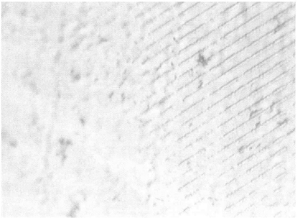
We did find generally better behavior as we lowered the exposure time. Both symptoms still occurred (sometimes on the same exposure), but with lower frequency. We progressed by reworking the actual sample about 5 times until we had a yield near 70% of the pixels.
The pixel quality could be judged quickly by the color at the lowest microscope magnification. If all pixels were red, then without fail, the PR would be patterned perfectly upon closer inspection. If the pixels were multicolored, we generally found poor gratings upon inspection with higher magnifications.
One possible suggestion is to try an anti-reflective coating (ARC) below the photoresist.
The second major issue with the gratings is the etch rate. Using two data points, we estimated the etch rate of the grating region using the CHTM ICP H2Anneal recipe to be about 2400 Angstroms per minute and the etch rate through the to be 920 Angstroms per minute. However, the etch rate for mask GDS1 and GDS2 are different because they have different groove widths. The etch rate of the gratings should be better characterized.
4 Removing the substrate
The task of removing the substrate required two practice rounds before we tried the last set of adjustments on the actual device. As described in the previous chapter, we used a 4:1 citric acid to wet etch.
The etching was performed in a 1000 mL beaker with about 500 mL of etching solution in the beaker. A magnetic stirring rod was used to improve the etch rate and etch uniformity. The etch rate is in the range of 0.2 microns per min to 0.4 microns per min. This gives a total etch time of nearly 36 hours.
During the etching, I would remove the samples from the etching solution, rinse and dry the samples, and measure their thickness with a micrometer.
Each time, before placing the samples in the etch solution, one should dip the samples into a solution of 1:10 to to remove the surface oxide. In principle, this should improve the etch rate uniformity across the sample.
I first practiced the etching on some samples mounted to glass slides with photoresist. I found the etch rate slowed with time. After 4 to 6 hours the etching solution needed to be replaced. During the last 10 hours of the etch, the photoresist broke free from the glass slide and the samples were etched away from both sides.
The next iteration involved mounting the sample to glass slides with melted wax. This time I was testing two different samples: a brag mirror with many 3000 Angstrom layers of AlAs, and a quantum-well structure with a single 300-Angstrom etch-stop layer of AlAs. When the sample was less than 10 microns thick, the brag mirror crumbled. I suspect the crumbling was due to the stress of the oxide formed in the reaction with the AlAs layer[8].
On the quantum-well sample, I saw the rough surface turn into a mirror-like surface over the course of four hours. The mirror-like surfaces would start as small spots at random locations on the surface and grow. When the surface was 90 % mirror-like, I removed it from solution. Visually the surface looked smooth with small discolorations. An alpha step scan revealed that the etch stop layer had broken through and the etching had again paused on the AlGaAs forming the barriers of the quantum wells.
We needed to improve the etch rate uniformity or decrease the amount of wet etching necessary to remove the substrate. Our solution was to lap 400 microns from the substrate before performing the wet etch. With this additional step, we removed the substrate trivially. The surface turned from rough to mirror-like in less than 5 minutes.
The substrate removal revealed a few indications of the wafer-fusion quality. The substrate removal revealed that the windows buried between the two epilayers had warped the epilayer above it into a 0.3 micron arroyo. Second, during a buffered oxide etch (BOE) dip to remove the AlAs etch-stop layer, the epilayer above one pixel popped off.
5 Etching the
Three approaches were considered for etching the . First was an ICP chlorine-based etch. This etches GaAs twice as fast as the . Although a small etch into the GaAs would not be disastrous for the process, the combined uncertainties of our etch rate in the ICP made this less desirable.
A second possibility is to use a BOE etch. I tried using a 90 second 1:20 BOE etch on three occasions on practice wafers. On two occasion, the BOE etched the large contact strips without difficulty, but did not etch the small 15 micron holes on the middle mesa that are needed to make contact with this layer. The third occasion will be discussed in the next paragraph.
The final method considered was a Reactive Ion Etch (RIE) with . This process worked beautifully on three trial samples. For a 100 watt plasma, and 100 mTorr of , the etch rate appeared to be more than 300 Angstroms per min. When we placed our actual, offical sample in the RIE, we found the process was etching more strongly on the edges near the mesa walls. Figure 5 shows the etched away to the walls. We believed the etching on these edges was due to residual attacking the number of sharp corners in the photoresist near this corner.
On the third re-work of this step, we tried purging the from the RIE exensively. During the conditioning runs, with the main valve behind the RIE shut off, we opened the line in the RIE to evacuate the pipe of all . We also did a 30 minute conditioning run. Before the etch, we performed 8 pump-and-purge cycles to remove the atmospheric .
During the actual etch, we ran out of . Under a microscope, the etch rate was observed to be highly non-uniform, but the edges near the mesa walls were untouched. Because we did not have an option to get more for several weeks, we choose to finish the etch with a one-minute etch in 1:20 BOE. About 80% of the appeared to have cleared, but about 20% was still a brown or blue color. After much concern, we proceeded with the process for depositing the bottom and middle contacts.
As we discuss later in this chapter, the device exhibited open-circuit behavior on all devices. will form an insulating barrier for 5 volts with as little as 50 Angstroms [22]. For a thickness of 50 Angstroms, the will appear the same color as the semiconductor. We could have a small layer of insulating our substrate from our metal contacts.
To use or not to use , that is the question. The Reactive Ion Etching (RIE) of the was done with a plasma. Other users use a small amount of in the RIE plasma. The reason is the etching process tends to leave behind organic compounds 11 1 I would like to thank Capt Chris Morath at AFRL/SN and Dr. Gabriel Font-Rodriguez at the US Air Force Academy for bringing this concern to my attention.. The small amount of is intended to remove the organic compounds from the surface. As shown in figure 5, adding to the during the RIE etch will not work for our process. One possible solution is to first perform the etch, then after purging the system and removing the photoresist, to do an plasma clean.

6 Driving metal up the mesa walls
The original plan was to use a wet etch for the bottom mesa. The reason was to create a slopped side wall that would facilitate the metal climbing up the mesa wall to make contact with the middle layer. The wet etch was supposed to be nearly isotropic to make these slopped side walls.
We tried several variations of a wet etch in of concentration 1:1:45. We tried with and without a magnetic stirring rod and we tried a stronger concentration of 1:1:15. The etch rate was very non-isotropic. The solution appeared to be etching laterally a factor of 40 times faster than the etch rate downward.
Instead of the wet etch, we decided to do a straight wall ICP etch and mount the sample in the metal evaporator at a small angle. The samples were mounted on the rough side of a Si wafer and loaded at an angle of 5.5 degrees such that the wall that the metal was going to climb was facing the oncoming particle flux.

This technique has shown mixed success. Figure 6 shows our success in getting the metal to climb the wall. However, on all three iterations that we tried this process, the lift-off procedure was difficult. In two cases, the lift-off procedure also removed metal that was intended to stick to the surface, and left metal where it was suppose to be removed. On one iteration, the lift-off procedure completely removed all the metal leaving nothing.
I think the cause for these complications is the metal-flux angle is overshooting the angle of the undercut of the photoresist. Metal lift-off is best performed with image reversal photoresist. The image reversal leaves the photoresist with an undercut that forces clean breaks in the metal deposited on the surface from the metal deposited on the photoresist. If during the metal deposition, the sample is slopped at an angle higher than the undercut, then the metal will climb up the photoresist walls and tie the two layers together.
To verify that the angle was responsible for the difficulties, we processed other samples in parallel with our sample. For the other samples that were loaded flat in the metal evaporator, the lift-off procedure was smooth and uneventful. The metal was all lifted-off within about 2 minutes using the acetone spray brush. For the polarimeter loaded at a 5.5 degree angle during the same run, lift-off involved more than 30 minutes with the acetone spray brush. The resulting metal deposited was partly a success but also had many regions of metal lifted-off that were suppose to stay and many regions of the surface with metal that was suppose to be lifted off.
Adhesion to the was also considered a potential source of difficulty. On the final metal evaporator run with the official sample, we tried using a 50 Angstrom layer of titanium to improve the metal adhesion to .
7 Wire bonding
Once the metal was annealed, we proceeded to wire bond the structure. The middle-layer contact pads required care to bond to. If the wrong temperature was used, the metal would rip from the insulating it from the bottom contact layer. Patience was the key for bonding these structures.
The top contacts were more difficult. Each time a wire bond was made to the top surface, the bond would break loose, and the contacting metal surface would disappear. Closer inspection with an SEM revealed the source of the difficulty. Figure 7 shows one such example of a pixel where the attempt to bond to the top contact failed.

Every top-contact to which a traditional wire-bond was attempted resulted in the failure of the fused interface. The wire bonds were adhering to the top metal contact pads without difficulty, but they were breaking off the fused epilayer.
Sunil Raghavan was able to make contact to the pixels despite this complication. The solution involved a conducting epoxy and can be seen in figure 3.
8 The failure of ohmic contacts
After the device was wire bonded, we tested the structure with a semiconductor parameter analyzer. Every pair of contacts, including the ground to ground contacts, showed an open behavior at room temperature with resistances greater than 1 giga ohm. A typical QWIP device at room temperature has a resistance near 10 to 20 ohms.
Where we had multiple contacts on a single ground strip, we would get the expected short like behavior with resistance less than 1 ohm. This verified the set-up and wiring diagrams were correct. The resistance of a quantum-well structure rises as one lowers the temperature.
To test the quality of the ohmic contacts, we used the ohmic contact probing mesas. Probes were placed on the top contact probing mesa. The current did not need to do anything different from entering the n-doped layer and leaving the n-doped layer 100 microns away. The resistance was still greater than a giga ohm. Unfortunately the middle and bottom ohmic contact probing mesas did not have any metal due to the difficulties during the metal lift-off procedure.
There are several possible causes for the failure to form ohmic contacts.
One possible cause is remained on the surface due to the difficulties we had removing it. will form an insulating barrier for 5 volts with as little as 50 Angstroms [22]. For a thickness of 50 Angstroms, the will appear the same color as the semiconductor. We could have a small layer of insulating our substrate from our metal contacts.
Another possibility is the RIE etch left a small layer of organics on the surface that is insulating the metal contacts from the n-doped surface. If this is the case, no amount of etching will remove this layer without use of some . Perhaps after the etch with , a very pure plasma will ensure the surface is free of an organic insulator. Pure plasma should not attack the so long as there is no residual .
A third possibility is the Si doping is not enough to form good ohmic contacts. To evaluate this, we should process a much more simple structure and evaluate the quality of the ohmic contacts.
9 Characterization setup
Also as a part of the project, at AFRL/VS, we validated an approach to characterize the polarimeter. A wire grid polarizer was inserted in-between a monochometer and the dewar window. A known QWIP sample with a linear grating was placed in the dewar. We measured the photocurrent as a function of polarizer angle. This experiment showed that the photocurrent was related to the angle of the polarizer in complete agreement with theory.
10 Suggestions for future processing rounds
The good news: at the end of the first round of processing, the physical structure on the chips is the desired physical structure. Figures 3, 6 and 7 show two quantum-well stacks and two gratings with one grating is buried in between the two quantum-well stacks. This is itself a substantial accomplishment.
For the next round of processing, I have the following suggestions.
- 1.
Test the quantum-wells and the contact layer of the wafer with a simple structure.
- 2.
Characterize the photoresist AZ5206 better or try a different photoresist. Some suggested an anti-reflective coating could help.
- 3.
Better characterize the etch rate of the gratings.
- 4.
Test for residue left from the RIE etch of the . Build a test structure with an n-doped GaAs surface. Deposit . Etch the holes, and deposit metal. Test for conduction through the n-doped GaAs.
- 5.
Test if the metal climbs the walls without the lift-off complications at a smaller angle (3 degrees for example).
Chapter 5 Conclusions
This thesis reported on a new optoelectronic device to detect, simultaneously and instantaneously, the four parameters that fully describe the polarization state of an ensemble of incident photons in a narrow wavelength band.
In chapter Model And Fabrication Of A Proof-Of-Concept Polarimeter-In-A-Pixel, I introduced the Stokes parameters as a way of fully describing the polarization state of incident light. I also introduced polarimetric imaging, and I reviewed other techniques for capturing polarimetric images. Other techniques involve large errors at the edges of objects in the scene or require the designer to sacrifice spectral resolution or increase the weight by using beam splitters and multiple focal plane arrays.
Chapter 1 introduced my solution to this difficulty. The new device uses the interference between multiple diffractions and reflections in the structure to encode in the multiple photocurrents the polarimetric information.
A computer model, developed in chapter 2, demonstrates the device’s preliminary polarimetric capabilities. The chapter describes the methodology of the model, reviews data generated by the model, and analyzes the data to gather worst-case performance estimates.
Finally, in chapters 3 and 4, I explain our approach and progress in building the device. These sections reviewed the overall approach, the wafer-fusion process, the substrate removal process, and recounted the difficulties we had in building the device: the difficulty with etching the gratings, the difficulties with etching the , and the difficulty with the metal lift-off. The final product did not have ohmic contacts into the device. I also listed a few possible explanations for this failure: an insulator was left on the surface or the contact layer’s doping is too low. Appendix 6 will enumerate the detailed processing recipe that I suggest for future fabrication attempts.
The polarimeter-in-a-pixel will be a totally new type of optoelectronic sensor. This is the first sensor that detects all the polarization information on a single physical pixel. The first round of fabrication brought into focus many hurdles that we overcame in building the physical structure. I expect that after solving the problem with the ohmic contacts, the concept for the device will be successfully validated.
Appendices
Chapter 6 Suggested processing recipe
Procedure for processing the Polarimeter-in-a-pixel:
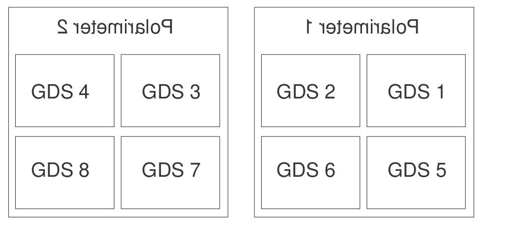
- 1.
Prepare the surface for wafer fusion.
Clean surface of tweezers, and both wafers. This is the most critical step for successful wafer fusion. A 5-minute acetone soak (to remove organics), A 5-minute isopropanol soak (to remove acetone), A 5-minute soak in running DI water (to remove isopropanol residue). Dip into 1:5 HF for 30 seconds to remove native oxides formed, then a 5-minute soak in running DI water to remove the HF and allow safe handling of the wafer. Now a 20 second dip in 1:30 NH4OH : H2O. Immediately blow dry (removes last of oxides) and place in PECVD vacuum in less than 10 minutes to beat oxide re-growth.
PECVD: Deposit 2000 Angstroms of Si3N4 oxide on both wafers to protect the clean surface. Use a surface temperature = 300 C, an operating pressure of 500 mTorr, use N2 flow = 85 sccm, NH3 flow = 12 sccm, SiH4 flow = 65 sccm, RF Power = 55 watts. It should take about 17 minutes for 2000 Angstroms to grow. Let the sample cool to 150 C before removing from the chamber.
- 2.
Photolithography (this step is still producing a 70% pixel yield, and needs to be further refined). Only one of the two wafers needs this photolithography.
Clean the surface. Note humidity and temperature. Again a 5-minute acetone soak and an acetone spray brush (to remove organics). Swirl the acetone constantly. Next, a 5-minute isopropanol soak (to remove acetone), again swirling constantly. Now a 5-minute soak in running DI water (to remove isopropanol residue). Blow dry the sample.
Dehydration Bake: 150 C for 7 min. Cover surface with HMDS, spin at 5k for 30 seconds. Bake on hotplate 150 C for 30 seconds. Add positive PR AZ 5206 to the wafer. Beth recommended this PR because it produces a more thin coat to get sharp grating features. Spin at 5k, 30 seconds. Check for photoresist that climbed over edge onto bottom. If found, restart step 2.
Softbake 90 C for 90 seconds. Remove edge beads (optional). If you do remove edge beads, use the edge bead removal mask. Expose between 3.5 and 5.7 seconds. Develop for 80 seconds in 1:5 AZ400 developer. Use the Dielectric-Grating mask (a negative mask) located on GDS-1. See figure 1 for more mask location.
- 3.
ICP Etch of the dielectric grating through the .
We need a reproducible etch depth known depth to within 0.02 microns. Our two-point calibration showed that using the H2Aneal recipe the etch rate in is 926 Angstroms per min. For 2000 Angstroms, the etch time is 2.1587 min. After etching the one needs to etch the GaAs. The etch rate is about 2410 Angstroms per min. With a desired depth of 8800 Angstroms, the etch time is an additional 3.65 min.
Total etch time is 5.81 min = 5 min 49 seconds.
Next we remove the photoresist with an acetone spray brush, followed by standard cleaning.
Standard cleaning is a 5-minute acetone soak and spray (to remove organics). Next a 5-minute isopropanol soak (to remove acetone). Now a 5-minute soak in running DI water (to remove isopropanol residue). Blow dry.
You will probably need to use an plasma to remove the remaining photoresist from surface. After the plasma, repeat the above cleaning procedure with soaks in acetone, IPA, DI water, and blow dry.
- 4.
Wafer fuse the samples.
In the case of this thesis, we shipped the samples to Lincoln Lab Attention Dr. Z. Liau MIT Lincoln Laboratory 244 Wood Street, Lexington, MA 02420-9108. He is doing this as a first-time small effort favor, and will probably not be able to perform wafer fusion on a regular basis without some funding support.
Wafer Fusion begins with removing Si3N4 protective layer with BOE wet etch. Use about 1 minute and 30 seconds of BOE 1:20 to remove the 2000 Angstroms of .
In this run, the wafer fusion was performed for 16 hours under 550 C and pressure.
- 5.
Lapping substrate of wafer down to about 75 to 100 microns.
- 6.
Remove substrate from wafer 2.
The substrate to be removed is from the wafer which has never been etched. Measure sample thickness with an electronic micrometer.
Perform a standard clean. Next dip in NH4OH : H2O 1:10 for 45 seconds to remove surface oxides, rinse in H2O and Blow dry. Mount the sample on glass slide with wax. Place side of wafer not to be etched closest to the glass. Mounting on the slide is performed by heating a slide up to 112 C; melt wax on slide; place wafer with protected substrate face down onto the wax; slide around until one can tell no bubbles remaining (look through bottom). After wax cools, measure thickness of sample on the slide - Mix by weight 1:1 dry Citric Acid Monohydrate and deionized water ( 250 grams, 250 grams) - Mix by volume 4:1 Citric Acid : . Place a magnetic stirring stick under a small platform in beaker. Pour 4:1 solution into the beaker. Etch rate is some where 0.25 to 0.35 microns per min, monitor thickness throughout etch and adjust endpoint accordingly. Replace the solution every 2 to 4 hours because the H2 will lose its potency. Last, remove the 300-Angstrom AlAs etch stop layer with a 60 second etch in 30:1 BOE solution.
- 7.
Photolithography
Use standard recipe for CHTM cleanroom to add 5214-IR Photoresist to newly exposed episurface. Expose using the Reflective-Grating (negative mask)-GDS-2 mask pattern. See figure 1 for mask location. Alignment windows on the buried structure should be visible in the microscope. Develop with standard time.
- 8.
ICP etch (etch rate needs to be recalibrated)
Make grooves 0.9 microns deep. Using the previously found grating etch rate for the H2Anneal recipie, a 9000 Angstroms etch at 2400 Angstroms per min = 3 min 45 seconds.
Remove the photoresist by acetone spray brush, followed by a standard clean. An plasma clean will probably be needed.
- 9.
Photolithography.
Add 5214-IR photoresist. Use the imager-reversal to optimize lift-off. Becomes a negative photoresist. Expose TopMetal (positive mask)-GDS-3 mask. See figure 1 for mask location. Develop.
- 10.
Deposit n-Metal. To aid in making contacts, use a very thick deposition. at least 4000 Angstroms if not more. Lift-off in with acetone spray brush.
- 11.
Photolithography
Add 5214 photoresist. Use the standard CHTM recipe for positive tone behavior. Expose TopPixelMesa (positive mask)-GDS-4 mask. See figure 1 for mask location. Develop.
- 12.
ICP etch of pixel mesa.
PR covering Au with little extra serves as mask (4.565 microns = (4.865-0.3) microns, etch slowly to get right stopping point) Etch rate 2700 Angstroms per min = 16 min 54 seconds.
Remove the photoresist with aceton spray brush. plasma will probably be needed.
- 13.
Photolithography
Add 5214-IR photoresist. Use standard CHTM image reversal recipe to make it a negative photoresist. Expose UpperMiddlePixelMesa (negative mask) GDS-5 mask. See figure 1 for mask location. Develop.
- 14.
ICP
Etch 1.0 micron - this will bring us 0.7 microns deep into the 0.9 micron gratings. @ 2700 Angstroms per min = 3 min 42 sec
Remove the photoresist with acetone spray brush. Standard clean. You will probably need to use an plasma to clean the remaining photoresist.
- 15.
Photolithography
Add 5214-IR photoresist using standard CHTM image reversal recipe. Expose LowerMiddlePixelMessa (negative mask) GDS-6 mask. See figure 1 for mask location. Develop.
- 16.
. ICP etch GaAs.
Etch 4.065 microns = 4.865-0.3 - 0.5. The first -0.7 is for the 0.7 microns of the bottom wafer etched by the 2nd ICP etch(this etch took away 1 micron, 0.3 from top wafer, 0.7 from bottom wafer). The next -0.5 microns is so that we stop short of the substrate and allow the bottom contact a conductive channel to the pixel.
At 2700 Angstroms per min this etch will be 15 minutes and 3 seconds.
Remove the photoresist, standard clean followed by an plasma to remove remaining photoresist.
- 17.
PECVD.
Deposit 2000 Angstroms of Si3N4 over whole surface. Use same recipie as in step 1. The dielectric breakdown field is at 8 MV/cm [22]. To allow bias of up to 10 V on 2nd QW, we need thickness greater than 125 Angstroms. The remainder is a factor of saftey and to ensure sidewall coverage.
- 18.
Photolithography.
Apply 5214-IR photoresist. Use image reveral to make it a negative Photoresist. Again use standard CHTM recipe. This type of photoresist allowed me to make the mask design with clear view of the pixels with which to align the mask. Expose with -Removal-mask (positive mask)-GDS-7 mask. See figure 1 for mask location. Develop This will exposes the patern that will open holes in the on the second layer, holes for the bottom contact, and holes in pixel top over the metal.
- 19.
RIE Selective Etch of Si3N4.
First clear out the in the pipe. Bring the RIE to about 10 mTorr. Now make sure the valve behind the RIE is closed, and turn on the switch on the RIE. Wait till the pressure returns to about 10 mTorr. Now close the swith on the RIE and perform a long conditioning run with CHF3. About 100 watts with about 100 mTorr pressure. 30 minutes should be enough. Now load the sample. Do eight pump-and-purge cycles to remove any from the atmosphere in the chamber. Now do the CHF3 etch for 9 minutes with the same settings as the conditioning run.
Now remove the photoresist with acetone spray brush followed by a standard clean.
Next do an clean. Again do an extensive purge of the system to remove any CHF3 in the chamber. Clear out the CHF3 pipe just as we cleared out the pipe in the previous paragraph. Do a 30 minute conditioning run. Now load the sample, do 4 pump-and-purge cycles, and do a 5 minute plasma clean. The plasma (if free of any CHF3) should not attack the and will remove only the organics left on the surface.
- 20.
Photolithography.
Use 5214-IR photoresist. Use the image reveral recipe so it becomes becomes a negative photoresist. Expose to LastMetalization (postive)-GDS-8 mask. See figure 1 for mask location. Develop
- 21.
Modified n-Metal deposition
First deposit use 50 Angstroms of titatium, then continue with the regular n-metal deposition. Lift-off using acetone spray brush, then perform standard cleaning.
- 22.
Put sample in rapid thermal annealer (RTA) to form Ohmic contacts
Treat in a rapid-thermal annealing system at 430 C for 1 min in the presence of N2/H2 forming gas, for the formation of good quality top, middle, bottom ohmic contacts.
- 23.
Mount the sample onto a back-side illuminated chip-carrier and wire bond.
References
- [1] J. Y. Andersson and L. Lundqvist. Near-unity quantum efficiency of AlGaAs/GaAs quantum well infrared detectors using a waveguide with a doubly periodic grating coupler. Appl. Phys. Lett., 59(7):857, 1991.
- [2] S. J. Andersson and L. Lundqvist. Grating-coupled quantum-well infrared detectors: Theory and performance. J. Appl. Phys., 71(7):3600, 1992.
- [3] K. Aoki, H.T. Miyazaki, H. Hirayama, K. Inoshita, T. Baba, N. Shinya, and Y. Aoyagi. Fabrication of 3d photonic crystal from 2d photonic plates by micromanipulation. Technical Digest. CLEO/Pacific Rim, pages I–14, 2001.
- [4] Daniel Beekman and James Van Anda. Polarization sensitive QWIP thermal imager. Infrared Physics and Technology, 42:323–328, 2001.
- [5] A. Black, A. Hawkins, N. Margalit, D. Bablic, A. Holmes, Y. Chang, P. Abraham, J. Bowers, and E. Hu. Wafer fusion:materials issues and device results. IEEE Journal of Selected Topics in Quantum Electronics, 3(3):943, June 1997.
- [6] Max Born and Emil Wolf. Principles of Optics. Pergamon Press, New York, 1975.
- [7] Dave Cardimona, Dang Le, Scott Gingrich, and Mario Serna. Advanced IR detector devices and concepts for remote sensing. Proceedings of the SPIE, 5152:316–326, November 2003.
- [8] Carrie Carter-Coman, Robert Bicknell-Tassius, Rudolph Benz, April Brown, and Nan Jokerst. Analysis of gaas substrate removal etching with citric acid: and for application to compliant substrates. Journal of the Electrochemical Society, 144:L29–L31, 1997.
- [9] Jay Van Delden. Ortho-babinet polarization-interrogating filter: an interferometric approach to polarization measurement. Optics Letters, 28(14):1173–1176, July 2003.
- [10] Arnold Goldberg, Theodore Fischer, Stephen Kennerly, William Beck, Vincent Ramirez, and Ken Garner. Laboratory and field imaging test results on single-color and dual-band QWIP focal plane arrays. Infrared Physics and Technology, 42:309–321, 2001.
- [11] Frank Iannarilli, Steven Jones, Herman Scott, and Paul Kebabian. Polarimetric-spectral intensity modulation (P-SIM): Enabling simultaneous hyperspectral and polarimetric imaging. SPIE Conference on Infrared Technology Applications XXV, 3698:474, April 1999.
- [12] J.Holloway, N. Witherspoon, N. Miller, K. Davis, H. Suiter, and R. Hilton. Navy/marine corps innovative science and technology developments for future enhanced mine detection capabilities. SPIE, 4038:1280–91, 2000.
- [13] Jong-Hee Kim, Dae Ho Lim, and Gye Mo Yang. Selective etching of algaas/gaas structures using the solutions of citric acid / and de-ionized / buffered oxide etch. Journal Vacuum Science Technology B, 16:558–560, 1998.
- [14] Yon-Lin Kok and Neal Gallagher. Relative phases of electromagnetic waves diffracted by a perfectly conducting rectangular-grooved grating. J. Opt. Soc. Am. A, 5:65–73, January 1988.
- [15] J. B. Lasky. Wafer bonding for silicon-on-insulator technologies. Applied Physics Letters, 48:78, 1986.
- [16] B. L. Levine. Quantum-well infrared photodetectors. J. Appl. Phys., 74(8):R1, 1993.
- [17] Z. L. Liau and D. E. Mull. Wafer fusion: A novel technique for optoelectronic device fabrication and monolithic integration. Appl. Phys. Lett., 56:737, 1990.
- [18] S. Lin, J. Fleming, D. Hetherington, B. Smith, R. Biswas, K. Ho, M. Sigalas, W. Zubrzycki, S. Kurtz, and J. Bur. A three-dimensional photonic crystal operating at infrared wavelengths. Nature, 394:251, July 1998.
- [19] H. Liu, M. Buchanan, and Z. Wasilewski. How good is the polarization selection rule for intersubband transitions? Applied Physics Letters, 72, April 1998.
- [20] A. Locke, D. Sabatke, E. Dereniak, M. Descour, J. Garcia, T. Hamilton, and R. McMillan. Snapshot imaging spectropolarimer. Proceddings of the SPIE, 4481:64–72, 2001.
- [21] Near Margalit. High-Temperature Long-Wavelength Vertical-Cavity Lasers. PhD dissertation, University of California, at Santa Barbara, Department of Electrical and Computer Engineering, June 1998.
- [22] D. Mui, H. Liaw, A. Demirel, S. Strite, and H. Morkoc. Electrical characteristics of Si3N4/Si/GaAs metal-insulator-semiconductor capacitor. Applied Physics Letters, 59:2848, 1991.
- [23] K. Oka and T. Kaneko. Polarization mapping using birefringent prism. SICE, page 2581, 2002.
- [24] Janet Pan and Clifton Fonstad. Theory, fabrication and characterization of quantum well infrared photodetectors. Material Science and Engineering, 28:65–147, 2000.
- [25] J. Peterson, G. Jensen, and J. Kristl. Imaging polarimetry capabilities and measurement uncertainties in remote sensing applicaitons. SPIE, 4133:221–232, 2000.
- [26] R. Petit. A tutorial introduction. In R. Petit, editor, Electromagnetic Theory of Gratings, Topics in Current Physics, pages 1–50. Springer-Varlag Berlin Heidelberg, New York, 1980.
- [27] F. Sadjadi and C. Chun. Machine recognition of objects using ir polarimetry. SPIE, 2756:53–59, 1996.
- [28] Martin Schmidt. Wafer-to-wafer bonding for microstructure formation. Proceedings of the IEEE, 86(8):1575, August 1998.
- [29] Mario Serna. Quantum-well detector concept for hyperspectral, coregistered, full-stokes-vector detection. Proceedings of the SPIE, 4823:113–120, 2002.
- [30] Mario Serna. Single-pixel polarimeter: Dielectric-gratings model and fabrication progress. Infrared Physics and Technology, 44:457–464, 2003.
- [31] S. Sposato, M. Fetrow, K. Bishop, and T. Caudill. Two long-wave infrared spectral polarimeters for use in understanding polarization phenomenology. Optical Engineering, 41:1055–64, 2002.
- [32] M. Tong, D. Ballegeer, A. Ketterson, E. Roan, K. Cheng, and I. Adesida. A comparative study of wet and dry selective etching processes for gaas/algaas/ingaas pseudomorphic modfets. Jounral of Electronic Materials, 21:9–15, 1992.
- [33] L. Wendler and T. Kraft. Theory of grating-coupler-assisted infrared spectrscopy of lower-dimensional electron systems: Local optics of anisotropic multilayer systems with grating. Physica B, 271:33–98, 1999.
- [34] L. Wernersson, K. Georgsson, A. Litwin, L. Samuelson, and W. Seifert. Planarization of epitaxial gaas overgrowth over tungsten wires. J. Appl. Phys., 79:500, 1996.
- [35] Noritsugu Yamamoto, Susumu Noda, and Alongkarn Chutinan. Development of one period of a three-dimensional phtonic cristal in the 5 micron wavelength region by wafer fusion and laser beam diffraction pattern observation techniques. Jpn. J. Appl. Phys, 37:L1052, 1998.
- [36] Z. H. Zhu, Feliz Ejeckam, Y. Qian, Jizhi Zhang, Zhenjun Zhang, Gina Christenson, and Y. Lo. Wafer bonding technology and its applications in optoelectronic devices and materials. IEEE Journal of Selected Topics in Quantum Electronics, 3(3):927, June 1997.