Testbeam characterization of a 3D silicon sensor read out by Timepix4
Abstract
Testbeam results from a 300 µm-thick 3D silicon sensor bump-bonded to a Timepix4 ASIC, are presented. The hit detection efficiency, spatial resolution, and timing performance of the 3D sensor are studied for several track angles, bias voltages and charge thresholds. The time measurements are corrected for Timepix4 clock-frequency variations and timewalk, while for the spatial studies, nonlinear charge-sharing corrections are determined. At perpendicular incidence, the time resolution of the 3D detector is equal to 245 ps with a hit detection efficiency. An optimal angle of with respect to the beam direction of the 3D detector was found, in which the time resolution improves by compared to normal incidence, while the hit detection efficiency reaches above and the spatial resolution is approximately 7 µm. Intrapixel studies show that a time resolution of 153 ps at the most probable value of the signal charge can be achieved for hits between the electrodes at normal incidence, while the timing performance of these best-performing regions deteriorate upon sensor rotation. The timing properties at different depths of the 3D sensor have been investigated with tracks at grazing-angle incidence, revealing a dependence of the time resolution along the sensor depth.
1 Introduction
The upcoming High Luminosity Large Hadron Collider (HL-LHC) [7] will pose significant challenges to particle detectors, which will have to cope with the increased number of quasisimultaneous proton-proton collisions. In particular, the LHCb Upgrade II Vertex Locator (VELO) [10] will require excellent spatial and temporal resolutions to correctly associate tracks with the collision vertices where they were produced. A per-hit time measurement with a resolution on the order of 50 ps [4], enabling four-dimensional (4D) tracking, and a spatial resolution better than 10 µm are targeted. Both are essential to discriminate between primary and displaced secondary vertices in such an environment, which are a distinct feature of beauty and charm hadron decays. These requirements, together with the high radiation levels expected at the HL-LHC, motivate the exploration of fast and radiation-hard sensor technologies. Among the proposed solutions under consideration for the Upgrade II VELO, three-dimensional (3D) silicon sensors constitute a promising sensor technology for fast and radiation-tolerant tracking detectors.
Silicon sensors with 3D electrode configuration have electrodes vertically embedded into the silicon bulk. In this way, the drift is decoupled from the substrate thickness, allowing for shorter drift lengths of the charge carriers without compromising the signal amplitude. In 3D sensors, the pixel pitch determines the drift distance, which can be minimized to ensure high charge collection efficiency even in the presence of severe charge trapping in the bulk. Three-dimensional sensors have demonstrated radiation hardness up to fluences of 11017 1 MeV neq cm-2 [1].
Three-dimensional pixel sensors are inherently fast devices, since the short drift path of charge carriers, perpendicular to the electrodes, also results in fast charge collection times. By decoupling the directions of charge deposition and collection, Landau fluctuations in the total generated charge take place along the direction of the track and to first order only affect the signal amplitude, which can be accounted for by timewalk corrections. Therefore, the impact of Landau fluctuations on timing performance, also known as Landau noise [24], is less significant in 3D silicon sensors. An important limitation of 3D sensors with columnar electrodes arises from spatial non-uniformities in the weighting field [12]. In this respect, more uniform weighting fields can be achieved by replacing columnar electrodes with trenches or by exploring multiple readout 3D electrode configurations, such as the two electrode (2E) geometry [20].
Single-pixel 3D test structures with fast discrete readout channels have demonstrated time resolutions on the order of tens of picoseconds [16, 1], while the scalability and maintenance of this performance in pixelated devices integrated with a readout chip remain to be studied. In 3D sensors, the length and diameter of the electrodes, which are correlated by the achievable aspect ratio [17], increase the sensor capacitance and consequently the electronics jitter. Optimal design and development of a 3D sensor with enhanced timing capabilities and minimal capacitance are therefore of great importance, and efforts are being made in this direction [19, 11].
This article presents the spatial and timing performance of a 3D silicon sensor [23] bump bonded to, and read out by, a Timepix4 application specific integrated circuit (ASIC) [18]. The characteristics of the specific 3D sensor and the key features of the Timepix4 ASIC are introduced in section 2, while in section 3 the experimental setup is described. In section 4 the application of corrections and the resulting spatial resolution of the 3D sensor are reported. A comprehensive study of the timing performance is presented in section 5, where the time resolution for particles crossing at perpendicular, small-angle, and grazing-angle incidences are discussed in detail. The conclusions are summarized in section 6.
2 Detector under test
The fabrication of 3D silicon sensors is based on deep reactive ion etching (DRIE) [17], where cylindrical holes or trenches are etched through the wafer and filled with heavily doped p-type and n-type material to form an active edge electrode. The 3D sensor used in this study is a 3D double-side double type column (3D-DDTC) sensor with partially through electrodes [27] and one electrode (1E) configuration [20] fabricated at IMB-CNM [22]. A schematic illustration of the sensor is presented in figure 1. From the front side, the etched holes are filled with highly p-doped polysilicon and, since they are formed on a 300 µm Si-n substrate, they are referred to as junction electrodes. The highly n-doped pillars from the backside are called ohmic electrodes. An active silicon depth of 70 µm below the junction electrodes and 60 µm below the ohmic electrodes is present. With a nominal diameter of the etched hole of 10 µm, a high aspect ratio was achieved, minimizing the ineffective regions within the sensor volume. The ohmic pillars on the backside of the sensor are interconnected through a highly n-doped polysilicon layer, forming a common electrode to which the bias voltage is applied. The frontside electrodes form pixels that are individually connected to the readout channels of the Timepix4 ASIC [18]. For this reason, the junction electrodes are hereafter referred to as readout electrodes and the ohmic ones as field electrodes. The 3D sensor under study was initially bonded to a Timepix3 ASIC and the results of its performance can be found in [14]. Recently, it was transplanted to a Timepix4 ASIC which is read out by a SPIDR4 readout system [26].

The Timepix4 ASIC is composed of square pixels with 55 µm pitch. For this study, the Timepix4 is operated in the ToA & ToT mode, in which both the Time of Arrival (ToA) and Time over Threshold (ToT) are registered for each hit. The determination of time is based on a system of local voltage controlled oscillators (VCOs) shared by groups of adjacent pixels, known as superpixels, running at a nominal frequency of 640 MHz. The 640 MHz VCO is activated when the preamplifier output crosses a set threshold value, and oscillates until the next rising edge of the 40 MHz global clock. The number of 640 MHz clock cycles is counted, providing a fine ToA (fToA) measurement with a nominal time to digital converter (TDC) bin size of approximately 1.56 ns. To improve the time resolution, four phase-shifted copies of the VCO are generated and their phases are captured at the rising edge of the 40 MHz global clock. In this way, the 1.56 ns period is further divided into eight bins, resulting in an ultra fine ToA (ufToA) measurement with a granularity of 195 ps. Therefore, Timepix4 provides a nominal TDC resolution of 56.4 ps, with ps being the best achieved [13].
For each hit, ToT is measured by counting the number of the 40 MHz clock cycles in which the signal remains above the threshold. The VCO is activated once again when the preamplifier output drops below the threshold, allowing a ToT measurement precision of 1.56 ns. Due to the nonlinear response of the front-end electronics in the energy range close to the threshold, the relationship between the registered ToT value and the charge generated in the pixel by an incoming particle is described by a surrogate function [15], given as the inversion of eq. 2.1.
| (2.1) |
The parameters of eq. 2.1 are determined independently for each pixel through a charge calibration procedure which is performed by controlled charge injection (test pulses) into the analog front-end of each pixel in the range [, ], with a step of .
3 Testbeam setup
The present analysis is based on data collected during August 2024 and May 2025 at the SPS H8 beam-line facility at CERN [8]. The detector under test (DUT) was exposed to a mixed-hadron () beam at 180 GeV/c, delivered in 4.5 second-long spills containing a few million particles each. The Timepix4 beam telescope [3] was used as the track reconstruction system, providing a µm pointing resolution at the DUT position. A composition of stages at the center of the telescope, which enable translation and rotation around -axis (angle ) and -axis (angle ), hosts the DUT. A time-reference system composed of two microchannel plate photomultipliers (MCP-PMTs) [2] achieves a timestamp accuracy of about 12 ps, and is used to characterize the temporal performance of the DUT. The reconstruction of the telescope tracks is performed by the Kepler package, described in [5, 3].
4 Spatial resolution
The spatial resolution depends on a variety of factors related to the design of the 3D sensor, namely the pixel pitch and sensor thickness, but also on operational and external parameters, such as the charge threshold of the Timepix4 ASIC, the bias voltage applied to the sensor and the incident angle of the impinging charged-particle track. Understanding the spatial resolution of the sensor as a function of these parameters provides essential context for the timing analysis that follows.
For a charged particle traversing a silicon sensor, the generated electron-hole (eh) pairs may be collected by multiple neighboring pixels, which are grouped together following the algorithm described in [3] to form a cluster. The spatial resolution of the 3D sensor is estimated from the spatial residuals, defined as the difference between the intercept of the reconstructed incident track with the sensor and the charge-weighted position of the associated cluster. The width of this distribution is a convolution of the intrinsic spatial resolution of the 3D sensor and the pointing resolution of the telescope. Hereafter, the quoted spatial resolution is calculated as the standard deviation of the central of the residual distribution, with the pointing resolution of the telescope subtracted in quadrature.


The charge-weighted average of the hits in a cluster is a biased estimator of the true position at which a charged-particle track traversed the sensor [25]. This bias arises from inhomogeneities in the weighting field and the random nature of the charge-carrier diffusion, which results in a nonlinear relationship between the deposited charge and the measured pixel response. At small incident angles the induced signal in subleading pixels is predominantly from the lateral diffusion of the charge relative to the field, meaning that the charge sharing is particularly sensitive to these nonlinearities and results in a larger bias. Conversely, at larger angles a greater fraction of the signal in subleading11 1 The pixel that registers the largest amount of charge in a given cluster is referred to as the leading pixel, while all remaining pixels are referred to as subleading pixels. pixels is from charge liberated directly within those pixels, resulting in a smaller bias and a more linear relationship. Figure 2 compares the track position to the charge-weighted position for associated two-pixel clusters for both perpendicular and angled incident charged-particle tracks. Following the method in [6], a polynomial fit is performed to the average charge-weighted position as a function of intrapixel position, where the order of the polynomial is selected as that which minimizes the sum of squared residuals per degree of freedom of the fit, up to a maximum degree of nine. The resulting fit is used to correct for the observed nonlinearities, a procedure known as corrections, and is repeated separately for all clusters containing up to two hits in the and directions at each incident angle of the impinging charged-particle track. Figure 3 shows the distributions of spatial residuals before and after the corrections calculated from the fits displayed in figure 2, where a reduction in standard deviation of 7% and 12% can be seen for charged particles of perpendicular and angled incidence, respectively. The top-hat distribution in the residuals at perpendicular incidence is a result of the binary resolution of single-pixel clusters, while the central peak appears after the correction process to two-pixel clusters in which there is a large charge imbalance between the leading and subleading pixels. The asymmetry observed in the residuals distribution at angled incidence is a result of residual nonlinearities that are not fully corrected in the correction process.
The spatial resolution along the -direction as a function of track incidence angle for two values of threshold is shown in figure 4. The lower threshold of yields a significantly better resolution across all angles, as charge shared between neighbouring pixels that would otherwise fall below threshold remains detectable, allowing the charge-weighted clustering algorithm and correction process to more accurately reconstruct the track position. Furthermore, at higher thresholds the spatial resolution of single-pixel clusters is degraded due to an increased number of hits falling below threshold within the region below the readout electrode, resulting in double-peaked spatial residual distribution. At perpendicular incidence, the resolution is approximately µm and µm for the low and high thresholds, respectively. For the minimum threshold value with workable noise levels for this sensor () the spatial resolution improves with increasing spin angle, reaching a minimum of approximately µm at a track incidence angle of around , where charge sharing between two pixels is maximized. Beyond this angle the spatial resolution degrades slightly. In contrast, the spatial resolution at the high threshold of is much less sensitive to incident track angle, varying only between approximately µm and µm. This is again due to the charge shared in the subleading pixels being below threshold, reducing most clusters to single-pixel hits for which the charge-weighting clustering algorithm cannot be used, limiting the resolution to the binary single-pixel contribution.
The spatial resolution along the -direction at varying values of threshold and reverse bias for perpendicularly incident tracks is shown in figure 5. Due to the short inter-electrode distance in the 3D sensor, the depletion voltage is very low, and the sensor is fully depleted from about 5 V onwards. Consequently, the charge sharing and charge collection properties of the 3D sensor are mostly saturated beyond a bias voltage of 40 V, leaving the threshold as the dominant factor affecting the spatial resolution. The spatial resolution degrades with increasing threshold, from around µm at a threshold of to approximately µm at , again as a result of the progressive reduction of charge-sharing information as the shared charge in subleading pixels increasingly falls below threshold. Altering the reverse bias applied to the 3D sensor has a small effect on the spatial resolution at low threshold values, with this effect becoming increasingly smaller at higher thresholds. At low threshold, this is as a result of charge sharing in the neighbouring pixels through the lateral diffusion of the charge carriers as they drift towards the electrodes. The amount of lateral diffusion depends on the drift time of the charge carriers, which up to saturation, is governed by the electric field strength. This in turn, once the sensor is fully depleted, is proportional to the bias voltage applied. At higher bias voltages the drift velocity is greater, charge carriers reach the electrodes faster, and the amount of lateral diffusion is reduced. This results in a slight reduction in charge sharing and therefore a degraded spatial resolution at low threshold. This is true up to saturation of the charge carrier velocity, which occurs at approximately 40 V in this sensor, where increasing the bias voltage further has no effect on the spatial resolution. At higher thresholds, this effect is not observed, as the shared charge in subleading pixels is below threshold, regardless of the amount of lateral diffusion. Overall, the impact of the applied bias voltage is small.
5 Time resolution
The time resolution, , is calculated from the RMS of the central of the time residual distribution, as will be discussed in section 5.1. The time residual is defined as the difference between the measured hit time of the leading pixel of the DUT cluster and the reference time, . The DUT time measurement is corrected for VCO frequency variations and timewalk. The reference time is calculated as the average timestamp of the two MCP-PMTs with an uncertainty of approximately 12 ps that is neglected hereafter.

A 640 MHz VCO divides the 25 ns period of the 40 MHz clock into 16 TDC bins providing the fToA measurement, with a granularity of 1.56 ns, as mentioned in section 2. In an ideal Timepix4 ASIC, all VCO copies in the superpixels would be identical. However, variations in the process parameters of the VCOs during the fabrication of Timepix4, as well as voltage and temperature differences across the chip, lead to deviations from the nominal frequency. For this DUT, an average frequency of MHz is measured with MHz spread across the detector area. This frequency spread generates differences in the time measurements of up to 0.5 ns. The VCO frequency deviations can be calculated using testbeam data for pixels with a sufficient number of hits. In figure 6, the time difference between the measured hit time and the reference time in two example pixels is shown as a function of the fToA value. Assuming a superpixel frequency of 640 MHz, all points would have the same average time residual, within the statistical error, which would be associated with the pixel time offset. If the VCO runs slightly faster (slower) than 640 MHz, the TDC bins shrink (expand), more (fewer) oscillating cycles are completed, and the hit is falsely reported at an earlier (later) time. The relationship between the relative time delay and the fToA values can be parametrized as
| (5.1) |
where and are parameters fit to data (see figure 6). The advantage of determining VCO corrections for each pixel instead of superpixel is that second-order differences, such as pixel offsets (parameter ), can be determined. However, this approach requires sufficiently large samples of calibration data per pixel.
After the application of VCO corrections, time residuals must also be corrected for the timewalk22 2 The term timewalk refers to the charge dependence of the measured hit time introduced by the constant threshold discriminator. However, different effects such as variations in the drift velocity of the charge carriers, may contribute to the measured timewalk and cannot be resolved in this analysis. effect in order to determine the optimal time resolution of the 3D detector. The relationship between charge, , and the observed difference between the measured time, , and is modeled by the function
| (5.2) |
where the empirical parameters , , and are fit to data. Typically, the timewalk correction is modeled with a single set of parameters for the entire detector (hereafter global timewalk correction) or for a separate set of parameters for every pixel (per-pixel timewalk correction) . However, in the following analysis, a different approach for the timewalk correction, based on the hit position within the pixel (position-informed timewalk correction) , will be introduced and its performance will be discussed.
5.1 Perpendicular incidence

For incident charged particles, perpendicular incidence is determined by the set of () angles of the rotation stages for which the mean cluster size is minimized. The mean cluster size at normal incidence is equal to pixels, indicating that the geometry of the 3D sensor does not favor charge sharing. Since a significant percentage of a given cluster’s charge is captured by a single pixel, the pixel with the first registered time measurement in the cluster (also leading pixel for of the cases) is used to determine the time resolution.
The average relative delay between the DUT hit time, corrected for the VCO variations, and the reference time is shown as a function of the incident track position within the pixel in figure 7. The readout and field electrodes are identified as the regions within the pixel that exhibit large positive time delay. The large time delay below the electrodes is associated with the low charge generated in the corresponding regions, which is accounted for by the timewalk correction. In addition to this effect, the contribution of depth variations in the electric field to the drift time is discussed in section 5.3. Regions of the pixel cell with and without electrodes are drawn as contour lines in figure 7 and are defined conservatively to minimize contributions from transition regions and isolate the characteristic behavior of the regions of interest.
The most probable value (MPV) of the hit charge distribution depends on the particle’s impact position within the pixel. The MPV is measured to be for events in the region between the electrodes, and and in the region of field electrodes and readout electrodes, respectively. These values are around lower than the expected charge deposition of minimum ionizing particles at normal incidence in a 300 µm thick silicon sensor. The deviation between the measured and expected MPVs can be explained either by an active thickness of the 3D sensor less than 300 µm or by a bias in the charge calibration. The active thickness of the sensor is investigated by studying the cluster length of particles passing through the sensor at grazing angles in the range [, ] [9] and is measured to be µm, compatible with the nominal sensor specifications. A mismatch in charge calibration can be quantified by analyzing the spectrum of a 241Am radioactive source. The primary -ray peak at 59.54 keV [21] is translated into , assuming an average ionization energy of 3.6 eV in silicon. However, in the DUT this peak appears to be at , revealing a difference. This discrepancy can be attributed, at least partially, to the tolerance of the calibration capacitors in Timepix4, but a more thorough investigation is required to understand this effect.

Since there is a strong correlation between the generated charge and the intrapixel hit position of the tracks, a timewalk correction is derived in bins of the intrapixel area and applied globally to all pixels. This type of timewalk function is formulated according to eq. 5.1, but accounts for the track impact position in the 3D pixel and is therefore referred to as position-informed timewalk correction. In figure 8, the density distribution of time residuals for all events is shown, corrected for the VCO variations and with the position-informed timewalk method. The distribution is symmetric around zero and has long tails, which are caused by particles passing through one of the electrodes. A sum of two Gaussian functions with a common mean and different widths denoted by and is fit to the distribution. The need for the second Gaussian function is attributed to the existence of roughly two separate regions within the pixel, where a worse resolution is obtained close to the electrodes. The effective width of this distribution is estimated as
| (5.3) |
where is the fraction of the distribution described by the first Gaussian function. In figure 8, the effective time resolution of the 3D detector, operating at 65 V reverse bias and threshold, is ps. For reference, the RMS of the central of the same distribution results in a time resolution of ps, compatible with the fit result. For this reason, in the following analysis of different bias voltages and thresholds, the time resolution is derived according to the RMS value of the central of events in the time residual distributions.
A comparison of the time resolution given by the three different types of timewalk correction is shown in figure 9 (left). For a constant threshold value of and an increasing reverse bias voltage, the time measurements are corrected by a global charge-based, per-pixel or position-informed timewalk function. Interestingly, per-pixel timewalk corrections do not improve the time resolution compared to the global timewalk correction, whereas for some cases with limited statistics they may even result in worse performance. This can be explained by the effective removal of differences between pixel time offsets by the per-pixel VCO corrections. On the other hand, the position-informed timewalk corrections result in better time resolution as a result of less skewed residual distributions. The time resolution improves with increasing bias voltage due to stronger electric fields, resulting in faster drift of the charge carriers, with the diminishing improvement at higher voltages being consistent with the carrier drift velocity approaching saturation. The best time resolution in the 3D detector is obtained for the highest possible reverse bias that could be achieved before breakdown occurs, i.e. 65 V. For this voltage, the time resolution is equal to ps for the global timewalk correction and ps for the position-informed timewalk correction, leading to a relative improvement of .


In order to study the impact of the discriminator threshold on the time resolution, a threshold scan was performed. In figure 9 (right), the time resolution versus the charge threshold value is given for different reverse bias voltages, after the global timewalk correction was calculated and applied for each set of bias and threshold settings. The best performance of the 3D detector occurs at the lowest threshold value and the highest bias. With increasing threshold values, an increasing number of hits below the electrodes do not deposit enough charge to cross the threshold. In such cases, the time residual distributions are dominated by charged particles passing between the electrodes. Even with this effect, the time resolution at high threshold is still worse than at low threshold values. An estimate of the time resolution that could be achieved using only hits with high ToT, while the time measurement at a low threshold is maintained, has been obtained offline. By requiring a minimum ToT value equivalent to , events in the electrode regions are effectively rejected (see figure 10, right). The results of this analysis are shown by the dashed line on figure 9 (left), with a best time resolution of 180 ps. However, this analysis discards of the reconstructed clusters, drastically reducing the detection efficiency of the 3D sensor.

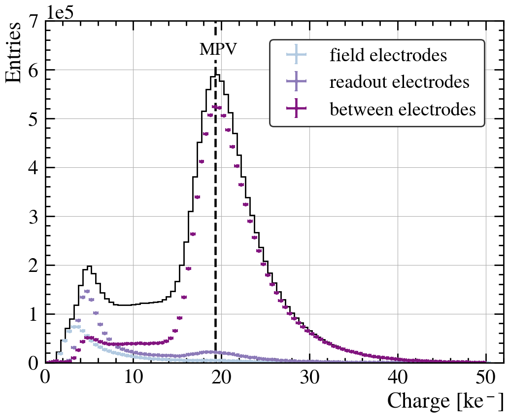
Figure 10 (left) shows the charge-dependent time resolution of the 3D detector at 65 V reverse bias and threshold after applying the position-informed timewalk corrections. Three different curves are plotted to distinguish the time behavior of the 3D sensor for events in the regions of field electrodes, readout electrodes, or between electrodes, following the definition of them in figure 7. These curves should be considered together with the charge distribution histogram in figure 10 (right). In a charge window around the MPV charge for events between the electrodes, , the time resolution is ps. Events in the same charge window, but with an impact position in the electrode regions instead, present a deteriorated time resolution of around 250 ps. This is not a timewalk-related effect but instead indicates variations in the weighting potential [12] and the drift field. At the MPV signal charge, the analog front-end jitter for the hole collecting mode (h+ mode) of the tested Timepix4 chip was measured to be ps, as shown by the black curve obtained with test pulse injection [13]. By adding the TDC and the analog front-end components in quadrature, the total contribution of Timepix4 to the time resolution is ps. Therefore, the time resolution is limited by the 3D sensor itself, in contrast to the reported timing performance of the exact same 3D silicon sensor on a Timepix3 ASIC in [14], where the main limitation was imposed by the analog front-end jitter of Timepix3. The time resolution is rather affected by the non-uniformity of the weighting potential in this 3D-DDTC configuration and variations in the drift field across the pixel.
5.2 Small-angle studies
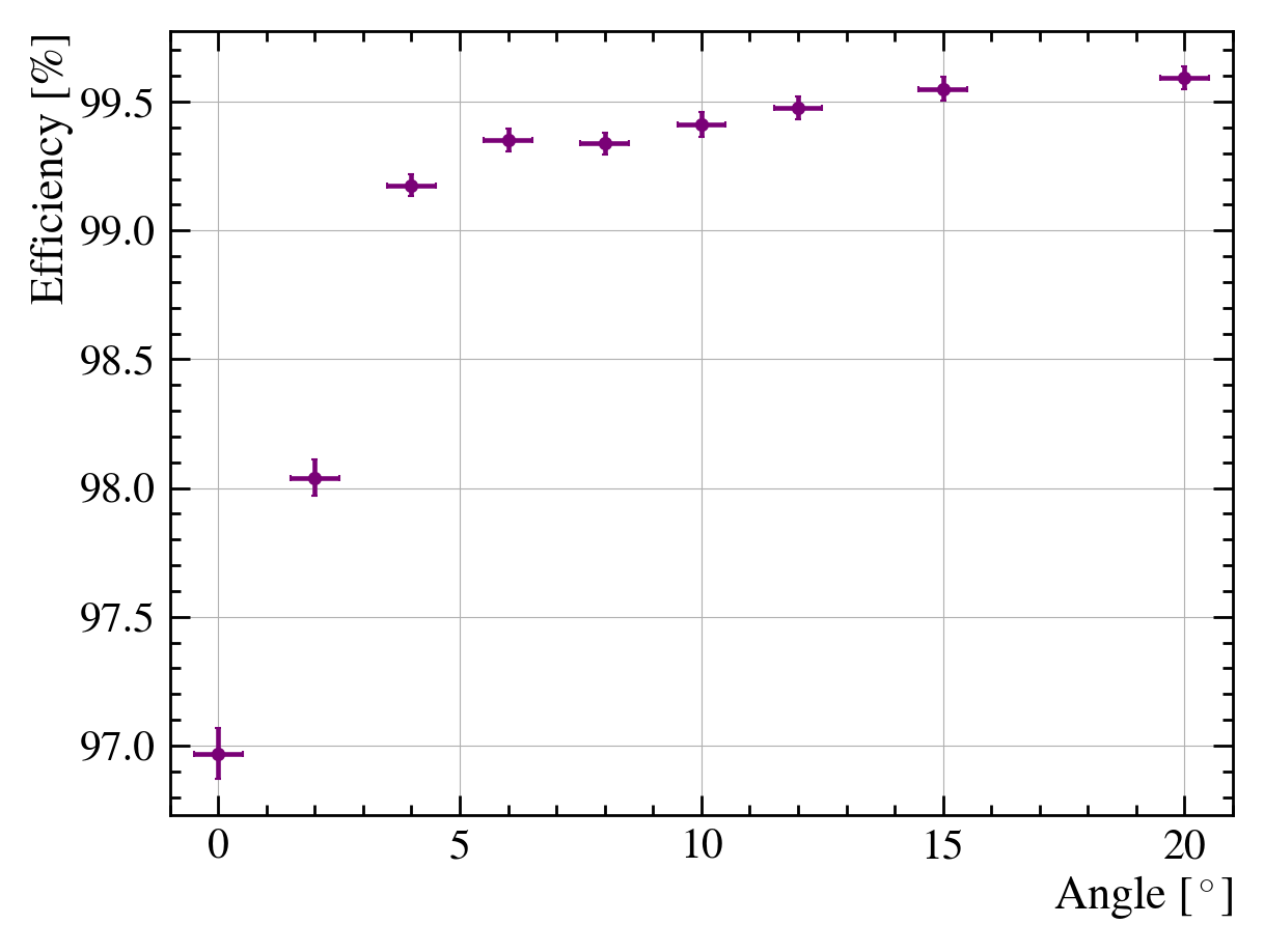
In 3D sensors, the electrodes are essentially regions of inactive volume, so if most of a particle trajectory passes through them, it will not be detected. A common solution to recover the geometrical efficiency of 3D sensors is to place them at an angle with respect to the beam direction. In this way, a significant fraction of all charged-particle tracks pass through the active silicon material of the detector, where they deposit some detectable charge. In the tested 3D-DDTC sensor, the problem of insensitive electrode regions is mitigated by electrodes that do not fully penetrate the bulk. In the regions below the electrodes, the traversing particles interact and deposit some charge. Therefore, the hit efficiency of the 3D detector under study for perpendicularly incident tracks at a reverse bias voltage of 60 V and at a threshold of is . According to figure 11 (left), the inefficiency mainly arises from particles going through the field electrodes, where charge sharing is more probable. As shown in figure 11 (right), a small rotation of the sensor, around , is sufficient to reach a hit detection efficiency above .

As discussed in section 5.1, tracks with a hit in the electrode regions are associated with worse timing performance due to the small MPV of deposited charge. Turning the sensor at a small angle also mitigates this problem and helps improve the time resolution across the entire pixel area. A qualitative illustration of how this works is presented in figure 12. The pixel is segmented into bins and the time resolution within the pixel area is shown for different angles (rotation around the -axis). The time measurements are corrected by the position-informed timewalk, where for each angle and bin a set of timewalk parameters is determined. Although this type of timewalk correction is expected to minimize the impact of the electrodes on time resolution, their presence is clearly visible in the top-left plot of figure 12. As the 3D detector is rotated, the poor time resolution in the regions containing pillars gradually vanishes, and the time response of the 3D sensor becomes more uniform inside the pixel.

To quantify the influence of the sensor rotation angle on the uniformity of temporal performance, the time resolution for different best-performing percentiles of the total pixel area is determined, as shown in figure 13. For each run, the bias voltage was kept at 60 V and the threshold value set at , while the angles were scanned in the range [, ]. Although the cluster size increases for larger angles, only the time information from the first hit is used and corrected by the position-informed timewalk. As shown in figure 13, even when considering tracks from the best of the pixel, the best timing performance corresponds to the normal incidence, at . However, for or of the pixel area, the optimal angle is . For of the pixel area, the time resolution is equal to ps at and ps at , marking improvement. While sensor rotation improves the overall time resolution of the detector, the timing performance of the best-performing pixel regions deteriorates.

5.3 Grazing-angle incidence
At grazing-angle incidence, the DUT stage is rotated around the -axis, placing the 3D detector almost parallel to the beam direction. The grazing angle method enables the investigation of the timing behavior for different depths from the sensor surface. A detailed explanation of this method is presented in [9]. Incoming particles enter from the backside of the 3D sensor, traverse multiple adjacent pixels, and exit from the frontside, where the bump-bonded ASIC is located. Each particle results in the formation of long clusters across multiple rows of the Timepix4 matrix. For a nominal rotation angle of the stage , the mean cluster length is pixels. The charged particles cross each pixel at a different depth, with the average depth for the th pixel, with respect to the minimum Timepix4 row of the cluster, given by
| (5.4) |
where a depth of 0 µm corresponds to the ASIC side, while a full depth of 300 µm corresponds to the backside.
In the case of fully passing-through columns in a 3D sensor, the electric field is independent of depth, neglecting surface effects. However, in this 3D-DDTC variation with partially penetrating electrodes, a -component (using the coordinate system defined in figure 1) of the electric field is introduced and becomes significant near the ends of the pillars. Three different -segments of interest can be defined: (i) µm, where the field electrodes are absent; (ii) , which corresponds to a fully 3D pillar configuration; and (iii) µm, where the readout electrodes are absent. For these three -segments, the hit charge MPV has been measured to be for µm, for and for µm. These values are lower than typical charge deposition in roughly 55 µm of silicon, but the aforementioned charge calibration mismatch as well as an effective width of the columns above 10 µm could explain the difference. Similar MPVs for µm and µm would be expected, since these segments are geometrically identical. However, a difference is observed, also for different bias voltages, and is attributed to the increased charge sharing in the µm segment.
At grazing-angle incidence, the charge is distributed relatively uniformly among the pixels in the cluster, and therefore no leading pixel can be selected for timing. The reference time is subtracted from the time measurement of each pixel, and VCO and timewalk corrections are applied. A global timewalk function, according to eq. 5.2, is calculated for this data. In addition, position-informed timewalk corrections are applied for different depths. The 300 µm thickness of the 3D sensor is segmented into 50 bands of 6 µm depth and, for each segment, a timewalk function is calculated. The corrected relative time delays versus the intercept are plotted for various bias voltages in figure 14 (left). An increase is observed for depths µm and especially µm, close to the surfaces of the 3D sensor. Although global timewalk parameters are used for this plot, the results do not improve when applying position-informed timewalk corrections. Since the MPV measurements indicate that charge is still generated at shallow depths, the slow charge collection suggests a lower drift-field strength. The absence of the opposite-type electrodes in these regions results in a low electric field [11]. The drift velocity of the eh pairs is small, and charges are partially collected by diffusion.
On the right side of figure 14, the time resolution at 60 V is shown as a function of the hit charge. Each curve corresponds to a specific -segment and the two different types of timewalk corrections are applied. Overall, the time performance of the 3D detector for depths is notably better than for µm and µm. For all hits in the -segment , the time resolution is equal to ps. This plot supports the same conclusion as figure 10 (left): hits in the electrode regions are produced at shallow depths and result in worse time resolution compared to hits between the electrodes, which are produced along the entire detector thickness.


The grazing angle method also offers the possibility to accurately timestamp passing charged particles by utilizing the time information provided by multiple pixels. A cluster time measurement can be extracted as the mean of the single-hit measurements, weighted by the charge dependent time resolution in figure 14 (right). If single-hit time measurements from the -segment of are used, and the index refers to individual pixel measurements, the cluster time is given by
| (5.5) |
where weighting by minimizes the error of the cluster time estimator. Considering uncorrelated single-hit time measurements with an average single-hit resolution , the time resolution of the cluster time measurement should scale with . However, some correlation between the single-hit time measurements might exist, since they all refer to a single 40 MHz clock and VCOs are shared in superpixels. This correlation is much stronger for perfectly even TDC bins. In reality, in Timepix4 VCO copies are not identical, as previously discussed, and variations in the TDC bin size, phase offsets between them, and potential differences of the charge carrier’s drift time act as a decorrelation mechanism for the single-hit time measurements. The dependence of the cluster time resolution on the number of hits, incorporating a correlation factor , can be approximated by
| (5.6) |
The cluster time resolution as a function of the number of hits used to calculate the weighted time is presented in figure 15. Performing a fit using eq. 5.6, a correlation factor of is found, indicating that hits are mostly uncorrelated. Despite the small value of the correlation, it has a strong impact on the cluster time resolution for large cluster sizes. The time resolution for clusters of 40 hits is approximately 170 ps, while for completely uncorrelated hits it is expected to be around 106 ps. Further investigations of these correlations are of interest for future 4D tracking ASICs as well as ultrafast timing detectors.

6 Conclusions
A 3D silicon sensor read out by a Timepix4 ASIC was evaluated in terms of its spatial and time resolution. The 3D detector was tested with a 180 GeV/c mixed hadron beam using the Timepix4 telescope at the CERN SPS H8 beamline. The data analysis encompassed corrections as well as corrections to compensate for the VCO frequency variations and timewalk.
The 3D detector has a time resolution of ps at a 65 V reverse bias and threshold. Charged particles with an impact position between the electrodes display a time resolution of ps, corresponding to a hit-charge MPV roughly of . Even for the best reported results, the dominant contribution to the time resolution is imposed by the 3D sensor, since the time resolution of Timepix4 ASIC in the hole-collecting mode was measured to be below 110 ps.
Rotating the DUT with respect to the beam direction benefits both the hit detection efficiency, as well as the temporal and spatial resolution of the 3D detector. At an optimal angle of , the time resolution improves by , while the hit efficiency increases from to . At the same angle, the best spatial resolution of approximately 7 µm is achieved for MIPs traversing the sensor, using a threshold of 0.8 ke- and -corrected charge-weighted clusters. This angle is found to give the optimal spatial resolution due to increased charge sharing between neighbouring pixels, corresponding to a charged-particle displacement across approximately one full pixel pitch. At the same time, most of the deposited charge remains confined to a single pixel, preserving large signal amplitudes that benefit the temporal resolution.
A further rotation of the 3D detector to a grazing angle of revealed worse timing performance at depths where opposite-type electrodes are absent. A brief study of the possibility of achieving better time resolution by combining single-hit time measurements was presented. The time resolution at grazing angle incidence is equal to 720 ps for single-hit time measurements and improves to 170 ps for a cluster size of 40, with correlation. A thorough understanding of the origin of these correlations could help mitigate their impact and potentially achieve a time resolution as good as the lowest achievable value for this ASIC.
The limitations in the measured time resolution can be attributed to several factors. An important limitation arises from the binary-like timing behavior observed, where regions between the pillars exhibit good time resolution, while the pillar regions show significantly worse performance. Reducing the electrode diameter would improve the ratio between these regions, although its impact on the weighting-potential uniformity should also be studied. In this context, alternative electrode configurations with multiple readout columns per pixel, such as the 2E geometry [20], one of the best candidates for the VELO Upgrade II, could provide a more uniform weighting field and improve the timing performance. However, additional electrodes increase the pixel capacitance and therefore the electronics jitter. The tested sensor is read out via p-type columns and requires the Timepix4 ASIC to operate in hole-collecting mode, while Timepix4 provides its best time resolution for electron-collecting sensors [18]. Future 3D sensors with n-type readout bonded to Timepix4 are expected to achieve improved results. Finally, in the tested 3D-DDTC design, the electric field depends on the sensor depth, introducing a spread in the drift velocity of the charge carriers. A 3D design with fully etched-through electrodes could reduce this spread and lead to a more uniform drift field, although this may come at the cost of increased capacitance and decreased hit efficiency. Overall, future studies could play an important role in optimizing 3D sensor design by balancing the aforementioned effects.
Acknowledgments
We express our gratitude to the CERN SPS accelerator team and beamline physicists for ensuring great performance of the SPS. We thank the LHCb testbeam coordinator, Loris Martinazzoli, for the support and coordination of the testbeam campaigns. We acknowledge the engineers who designed the Timepix4 ASIC. We gratefully acknowledge the support from the following national agencies: the Netherlands Organisation for Scientific Research (NWO), in particular this publication is part of the project FASTER with file number OCENW.XL21.XL21.076 and the Science and Technology Facilities Council (United Kingdom) including grant reference ST/@004305/1.
References
- [1] (2024) Characterisation of 3D trench silicon pixel sensors irradiated at 1 MeV n cm. Frontiers in Physics Volume 12 - 2024. External Links: Link, Document, ISSN 2296-424X Cited by: §1, §1.
- [2] (2004) MCP-PMT timing property for single photons. Nuclear Instruments and Methods in Physics Research Section A: Accelerators, Spectrometers, Detectors and Associated Equipment 528 (3), pp. 763–775. Cited by: §3.
- [3] (2026) The Timepix4 beam telescope. Nuclear Instruments and Methods in Physics Research Section A: Accelerators, Spectrometers, Detectors and Associated Equipment 1084, pp. 171234. External Links: ISSN 0168-9002, Document, Link Cited by: §3, §4.
- [4] (2022) Considerations for the VELO detector at the LHCb upgrade II. Technical report CERN. External Links: Link Cited by: §1.
- [5] (2019) LHCb VELO Timepix3 telescope. Journal of Instrumentation 14 (05), pp. P05026. External Links: Document Cited by: §3.
- [6] (2012) Charged-particle tracking with the Timepix ASIC. Nucl. Instrum. Meth. A 661, pp. 31–49. External Links: 1103.2739, Document Cited by: §4.
- [7] I. Béjar Alonso, O. Brüning, P. Fessia, M. Lamont, L. Rossi, L. Tavian, and M. Zerlauth (Eds.) (2020) High-Luminosity Large Hadron Collider (HL-LHC): Technical Design Report. Technical report CERN, Geneva. External Links: Document, Link Cited by: §1.
- [8] (2019) The H8 Secondary Beam Line of EHN1/SPS. External Links: Link Cited by: §3.
- [9] (2021) Temporal characterisation of silicon sensors on Timepix3 ASICs. Journal of Instrumentation 16 (07), pp. P07035. External Links: Document Cited by: §5.1, §5.3.
- [10] (2021) Framework TDR for the LHCb upgrade II. Technical report CERN, Geneva. External Links: Link, Document Cited by: §1.
- [11] (2012) Simulations of 3D detectors. PoS Vertex 2011, pp. 025. External Links: Document Cited by: §1, §5.3.
- [12] (2001) Review of the Shockley–Ramo theorem and its application in semiconductor gamma-ray detectors. Nuclear Instruments and Methods in Physics Research Section A: Accelerators, Spectrometers, Detectors and Associated Equipment 463 (1-2), pp. 250–267. Cited by: §1, §5.1.
- [13] (2022) Timing performance of the Timepix4 front-end. Journal of Instrumentation 17 (07), pp. P07006. External Links: Document Cited by: §2, §5.1.
- [14] (2021) Timing measurements with a 3D silicon sensor on Timepix3 in a 180 GeV/ hadron beam. Journal of Instrumentation 16 (08), pp. P08009. External Links: Document Cited by: §2, §5.1.
- [15] (2011) Precise energy calibration of a pixel detector operating in time-over-threshold mode. Nuclear Instruments and Methods in Physics Research Section A: Accelerators, Spectrometers, Detectors and Associated Equipment 633, pp. S262–S266. Note: 11th International Workshop on Radiation Imaging Detectors (IWORID) External Links: ISSN 0168-9002, Document, Link Cited by: §2.
- [16] (2020) Timing performance of small cell 3D silicon detectors. Nucl. Instrum. Methods Phys. Res., A 934, pp. 26–32. External Links: Link, Document Cited by: §1.
- [17] (2020) Deep reactive ion etching. In Handbook of silicon based MEMS materials and technologies, pp. 417–446. Cited by: §1, §2.
- [18] (2022) Timepix4, a large-area pixel detector readout chip that can be tiled on four sides, providing sub-200 ps timestamp binning. Journal of Instrumentation 17 (01), pp. C01044. External Links: Document Cited by: §1, §2, §6.
- [19] (2021) Timing optimisation and analysis in the design of 3D silicon sensors: the TCoDe simulator. Journal of Instrumentation 16 (02), pp. P02011. External Links: Document Cited by: §1.
- [20] (2025) Timing-optimised 3D silicon sensor with columnar electrode geometry. Sensors 25 (3). External Links: Link, ISSN 1424-8220, Document Cited by: §1, §2, §6.
- [21] NuDat 3: nuclear structure and decay data. Brookhaven National Laboratory. Note: Evaluated Nuclear Structure Data File (ENSDF), Am decay data External Links: Link Cited by: §5.1.
- [22] (2006) Double-sided 3D detector technologies at CNM-IMB. In 2006 IEEE Nuclear Science Symposium Conference Record, Vol. 2, pp. 1248–1252. Cited by: §2.
- [23] (2012) Characterisation of Glasgow/CNM double-sided 3D sensors. Physics Procedia 37, pp. 1016–1023. Note: Proceedings of the 2nd International Conference on Technology and Instrumentation in Particle Physics (TIPP 2011) External Links: ISSN 1875-3892, Document, Link Cited by: §1.
- [24] (2025) Time resolution limits in silicon sensors from Landau fluctuations and electronics noise. Nuclear Instruments and Methods in Physics Research Section A: Accelerators, Spectrometers, Detectors and Associated Equipment 1080, pp. 170808. External Links: Document Cited by: §1.
- [25] (1993) Spatial resolution of silicon microstrip detectors. Nucl. Instrum. Meth. A 335, pp. 44–58. External Links: Document Cited by: §4.
- [26] (2017) SPIDR, a general-purpose readout system for pixel ASICs. Journal of Instrumentation 12 (02), pp. C02040. External Links: Document Cited by: §2.
- [27] (2008) Double-sided, double-type-column 3D detectors: design, fabrication, and technology evaluation. Nuclear Science, IEEE Transactions on 55, pp. 2775 – 2784. External Links: Document Cited by: §2.