Tuning Andreev reflection and conductance in proximitized nanowires
through the spin-orbit field direction
Abstract
We investigate the Andreev reflection (AR) and the nonlinear conductance in a normal-superconductor junction realized with a proximitized semiconductor nanowire exposed to a magnetic field along its axis. We show that, while at zero energy the AR coefficient is determined by the topological phase of the superconducting side of the junction, at finite energy the AR is strongly affected by the directions of the Rashba spin-orbit field characterizing the normal and the proximitized sides. The tunability of the AR and the nonlinear conductance as a function of the spin-orbit misalignment angle is particularly pronounced when the proximitized side is in the topologically trivial phase. The spin-orbit field direction is revealed to be an efficient knob to control the electron transport through the hybrid junction, realizing an electrically widely tunable device. The implementation in realistic setups is discussed.
I Introduction
Semiconductor Nanowires (NWs) with strong spin–orbit coupling have emerged as a versatile platform to explore fundamental quantum transport phenomena and to engineer novel quantum devices. This is due to two important factors. First, owing to their quasi-one-dimensional geometry and high crystalline quality [31], NWs exhibit electron ballistic propagation [104, 18, 41, 103], allowing for the observation of phase coherent interference effects [24, 29, 9, 101, 97, 54] and quantized conductance [98, 44, 30]. Second, the Rashba spin–orbit (SO) field originating from structural inversion asymmetry (SIA) is tunable via electrostatic gates in different geometries [100, 49, 55, 95, 43, 81, 87, 89, 102, 46, 90, 27, 23, 15, 82, 42, 26], making NWs highly adaptable and particularly attractive quantum systems for studying spin-dependent transport at the nanoscale [92, 94, 93, 72].
Because of these remarkable features, NWs have found applications in multiple fields. In nanoelectronics, they serve as building blocks for field-effect transistors, with excellent electrostatic control and scalability [96, 83, 18, 88]. Also, their one-dimensional geometry and tunable carrier density make them promising candidates for thermoelectric devices, where quantum confinement can enhance thermopower and energy conversion efficiency [45, 34, 28, 60, 6]. Furthermore, by covering a NW with a superconductor, the interplay between the superconducting pairing induced by proximity effect, the Rashba SO field and an externally applied magnetic field realizes a topological superconductor [59, 66]. The Majorana modes predicted to emerge at the NW ends could have quite relevant applications in topological quantum computation [4, 1, 2, 84].
Although an unambiguous experimental evidence of the exotic Majorana quasiparticles is still a debated issue [86, 73, 17, 84, 71], the extensive effort devoted in their search has also boosted the investigation of hybrid NW devices, where only some segments of the NW are proximitized by a superconductor(S), while other segments remain unproximitized and are dubbed normal(N) [20, 63, 74, 22, 65, 21, 38, 103]. Various interesting effects emerge in such hybrid NW junctions. For instance, it has been theoretically predicted [67, 62, 32] and experimentally proven [91, 40, 39, 68, 7, 70, 69, 57, 58] that S-N-S junctions based on NWs can be harnessed to realize Andreev spin qubits, which can be readout and manipulated via microwave radiation. Also, such junctions can exhibit anomalous Josephson effect [16, 64] and, when voltage-biased, the resulting dc current can reveal information about the topological transition occurring in the S-segment [78]. Furthermore, recent studies on NW-based N-S-N junctions have revealed the competition between crossed AR and elastic cotunneling [13, 33].
At any N-S interface in a NW, spatial inhomogeneities in the SO field naturally arise. Indeed the SIA in the uncovered N-side differs from the one in the covered proximitized S-side, owing to changes in electrostatic screening, dielectric environment, to the geometry of gates coupled to the N-side, or to the way the superconducting film is deposited onto the S-side. Such inhomogeneities are expected to affect the AR process, since an incident electron from the N-side is reflected as a hole in a way that is sensitive to spin structure, which in turn depends on the SO field. Two types of inhomogeneity can arise across the N-S interface, namely in the magnitude and in the direction of the SO-field. The former type of inhomogeneity is expected to affect AR for trivial reasons: The magnitude of the local SO field directly modifies the spectrum of the related NW segment, giving rise to a potential step barrier at the interface. This effect already exists in normal NWs, where local inhomogeneities of the SO magnitude have been shown to affect the conductance and the spin density profile [80, 56, 79, 77, 14, 25, 76, 75]. For this reason, most experimental efforts have been devoted to enhancing the range of tunability of the SO magnitude, exploiting various gating techniques [55, 95, 43, 81, 87, 89, 102].
By contrast, the latter type of SO-inhomogeneity –in the SO field direction– is more subtle: Although it leaves the local spectrum of the NW segment unaltered, it does affect the electron eigenfunctions in a nontrivial way. Notably, while experimental advances have been made to control the SO field direction with suitable gating geometries, such as side or wrap gates [46, 90, 27, 23, 15, 82, 42, 26], or with a lateral deposition of the proximitizing superconducting film [12, 61], theoretical studies have analyzed this problem only partially so far, and mainly in two cases. On the one hand, in a normal NW, an antiparallel SO field configuration can realize a Dirac paradox configuration for electrons, which has been predicted to strongly reduce the conductance and to dramatically enhance the thermoelectrical properties of the NW [37, 36, 6]. On the other hand, in the presence of a superconducting pairing present in the entire NW, a SO direction inhomogeneity leads to trivial fermionic bound states that, at anti-parallel configuration, are degenerate with Majorana quasiparticles [48]. However, when it comes to hybrid N-S junctions based on NWs, the effects of the SO field direction inhomogeneities on the AR have not been investigated in details yet. Because the AR process is the fundamental mechanism governing the electronic behavior of hybrid quantum devices, understanding such effect is essential for interpreting experiments and for optimizing the hybrid device performance in applications, ranging from Majorana platforms to Andreev spin qubits.
This paper aims to address this problem. We analyze a N-S junction based on a single-channel NW, exposed to a Zeeman field applied along the NW axis, as depicted in Fig.1. We show that, while at zero energy the AR coefficient is purely determined by the topological phase of the superconducting side, at finite energy the AR and conductance are strongly determined by the SO field misalignment in the two sides of the interface. In particular, the trivial regime seems to be particularly suitable to yield a widely tunable AR and conductance at finite energy. These results indicate that the spin-orbit field direction can be harnessed as a knob to realize an electrically controllable hybrid device.
The paper is organized as follows. In Sec.II we present the model for a inhomogeneous proximitized NW. In Sec.III, after summarizing the main ingredients of the Scattering matrix method applied to the NW case, we present our results about the AR coefficient and the nonlinear conductance of the N-S junction, showing their dependence on the relative SO angle, for various values of the Zeeman field, exploring both the topological and the trivial phase of the S-side. Then, in Sec.IV, we discuss our results, provide an interpretation for the tunability of and , and propose implementation schemes in realistic setups. Finally, we draw our conclusions in Sec.V.
II Model for a proximitized NW with inhomogeneous spin-orbit field
We consider a single-channel NW deposited on a substrate and denote by the direction of its axis, by the other direction lying in the substrate plane, and by the direction perpendicular to the substrate, as illustrated in Fig.1. The NW Hamiltonian consists of four terms,
| (1) |
where
| (2) |
is the kinetic term in the effective mass approximation. Here, denotes the electron field operator for spin , while is the momentum operator, and denotes the chemical potential profile. The second term in Eq.(1) is
| (3) |
and describes the inhomogeneous Rashba SO coupling, characterized by a space-dependent SO vector field . The anticommutator term is necessary because does not commute with the momentum . Moreover,
| (4) |
denotes the Zeeman coupling with the applied magnetic field, whereas
| (5) |
is the superconducting pairing potential induced by proximity effect, which is assumed to vanish in the unproximitized N-side on the left of the interface, located at , while it is present in the NW proximitized side S on the right of the interface
| (6) |
By introducing the four components Nambu spinor field operator
| (7) |
the proximitized NW Hamiltonian Eq.(1) can be rewritten, up to an additive constant, in the Bogolubov – de Gennes (BdG) form [11, 35, 47]
| (8) |
where the BdG Hamiltonian
| (9) |
is characterized by a electron-block and a hole-block , mutually related by
| (10) |
and explicitly given by
| (11) | ||||
| (12) |
respectively. In Eqs.(11)-(12),
| (13) | |||||
describes the SO field operator. Note that, differently from the actual Zeeman field , the SO field is complex and, in particular, purely imaginary, i.e. .
Then, the BdG Hamiltonian (9) entails the BdG Equations,
| (14) |
where
| (15) |
is the eigenfunction, whose upper spinor and lower spinor refer to the electron and hole eigenfunction components, respectively.
II.1 Magnetic field along the NW axis and piecewise inhomogeneous spin-orbit coupling
While the inhomogeneous model in Eq.(1) is actually quite general, we shall henceforth make specific assumptions that suit for the N-S setup we aim to consider here. First, we shall consider the case where the magnetic field is applied along the NW axis
| (16) |
Second, recalling that the Rashba SO field is , where is the propagation wavevector along the single-channel NW axis and is the SIA electric field, one deduces that the SO field lies entirely in the plane perpendicular to the electron propagation direction (see Fig.1). This implies that the magnetic field and the SO coupling are mutually orthogonal. Third, we assume that the SO field can be fairly approximated by a piecewise constant profile
| (17) |
where and denote the SO fields in the N-side and in the proximitized S-side of the interface. The fields and can differ by magnitude and orientation. Without loss in generality, we shall take
| (18) | |||||
| (19) |
with , while describes the misalignament angle between the two SO field directions.
A piece-wise constant profile is also assumed for the chemical potential , with and denoting its values on the N and S-sides, respectively. As a consequence, the solution of the BdG equations (14) for the entire N-S system is expressed as a piecewise function
| (20) |
where (N-side) and (S-side) fulfill boundary conditions. Explicitly, while the wavefunction is continuous,
| (21) |
its derivative exhibits a discontinuity at the interface location , related to the inhomogeneity of the SO field (17)
| (22) |
Here, denotes the identity in Nambu space.
II.2 Excitation spectra and energy regimes in the two sides of the junction
Here, we briefly recall the main aspects characterizing the excitation spectra and the eigenstates in the bulk of each junction side.
As far as the bulk spectrum is concerned, it consists of the positive energy eigenvalues obtained by plugging a plane-wave solution into the BdG equations (14), where denotes a spinor. Specifically, on the N-side, the spectrum is
| (23) |
whereas on the S-side one finds [66, 59]
| (24) | |||||||
Here, , while the index denotes the two bands. Furthermore,
| (25) |
is the Zeeman energy related to the applied magnetic field, while
| (26) |
denotes the SO energy on the two sides of the hybrid junction.
We recall that the spectrum (23) on the N-side can exhibit two possible regimes [85, 64, 76], namely the Zeeman-dominated regime (), and the Rashba-dominated regime (), where the lower excitation band () exhibits a mexican-hat shaped behavior as a function of . In contrast, the spectrum (24) of the S-side is characterized by a superconducting gap at , closing at the critical value
| (27) |
The value is known to separate the trivial phase () from the topological phase () that hosts Majorana bound states at the S ends [59, 66]. Examples of the excitations branches in the bulks of the N and S sides are depicted in panels (a) of Figs.2 and 3.
When it comes to the bulk eigenstates on each junction side, as is customary in hybrid junctions involving superconductors, the excitation wavefunction can be also attributed a quantum number identifying the predominant electron(e)-like or hole(h)-like character of the excitation. Explicitly, denoting the spinor components for each band as
| (28) |
the sign of quantity
| (29) |
determines whether has an electron-like character (if ), or a hole-like character (if ). In the N-side, one has either or , corresponding to purely electron or purely hole excitations. In the Appendix A, the expressions of the resulting spinors are explicitly provided for both junction sides.
III Method and Results
In this section we shall present our results about the AR and the nonlinear conductance of the NW-based N-S junction. We start by observing that, because the SO energies (26) depend only on the magnitude of the SO field , a difference in across the interface directly affects the spectra (23) and (24) on the two junction sides, giving rise to an effective potential step. As mentioned above, such inhomogeneities of the SO magnitude have already been studied in normal NWs and, as expected, they can affect the transport properties and the spin density profile [80, 56, 79, 77, 14, 25, 76, 75]. By contrast, the eigenstates also depend on the direction of , through the spinor . Thus, due to the boundary conditions (21)-(22) of the wavefunctions, transport properties turn out to depend non-trivially on the relative angle characterizing the two directions in Eqs.(18).
The goal of our investigation is point out that such a dependence on is strong, and that it can be harnessed to tune the AR and the nonlinear conductance of the NW. Here below, after describing the method adopted to investigate the hybrid junction and defining the analyzed quantities, our results are illustrated.
III.1 Scattering Matrix approach
Our approach is based on solving the BdG equations (14) through the Scattering matrix formalism for hydrid normal/superconducting systems [52, 10, 8, 53, 50, 19, 5, 51]. To this purpose, we have complementarily combined analytical approaches and numerical methods, whose main ingredients are summarized here below, where we also specify the adopted notation. The interested reader can find further technical details in the Appendix B.
At a given energy , the wavefunction and on each side of the junction can always be expressed as a superposition of planewave eigenstates of the form . Each wave, weighted by a related complex amplitude, can be classified according to various quantum numbers. Indeed, for each band , various wavevectors are obtained by solving the equation [see Eqs.(23) and (24)], on each side of the interface. At energy , wavefunctions characterized by a real wavevector identify the propagating modes, which appear always in pairs because Eqs.(23) and (24) are even in . The sign of the group velocity identifies the propagation direction of the mode (rightwards or leftwards). Furthermore, at the energy , one can also have wavevectors with an imaginary part. Although such wavevectors always come in complex conjugate pairs , only the ones that do not imply an exponential divergence of their wavefunction at are physically acceptable and are the evanescent modes. Finally, modes at energy can further be classified as electron or hole modes on the N-side, and electron-like or hole-like modes on the S-side.
Henceforth, we shall label by the amplitudes of propagating modes that are incoming towards the interface, by the amplitudes of the modes that are outgoing from the interface, while the letter will be devoted to the amplitude of evanescent modes. Thus, each of these states is labelled by a quantum number set , where labels the side of the junction, the electron-like or hole-like character, while collects the band index and all the other possible different -values of that -type.
Explicitly, on the N-side, the wavefunction at a given energy reads
| (30) | |||||||
where the amplitudes and characterize right-moving modes incoming from the N-side towards the interface and left-moving modes outgoing from the interface into N, respectively, while labels the amplitude of the evanescent modes decaying at . In Eq.(30), denote the group velocities of the propagating modes, with momenta , while for the evanescent modes the momenta exhibit a negative imaginary part, and the velocity is formally introduced just to have the -amplitudes with the same units as the amplitudes and .
An expression similar to Eq.(30) holds in the S-side, upon an appropriate relabelling () in the amplitude coefficients. In particular, exhibits a positive imaginary part. For energies values below the superconducting gap of the S-side, which in general depends on and , there are only evanescent modes.
The boundary conditions (21)-(22) enable one to express all the amplitudes of the outgoing propagating modes and all the amplitudes of the evanescent modes in terms of the amplitudes of the incoming propagating modes. Details about this derivation are given in Appendix B. Denoting by and the vectors of outgoing mode amplitudes and incoming mode amplitudes in the lead , for particle nature , they are connected through the Scattering matrix as follows
| (31) |
Here, the entries of the block matrix describes the AR process where an electron state injected from the N-side gets reflected into a hole state available in N. Similarly, the block also describes an AR process, where hole and electron roles are interchanged though. The and blocks account for the normal electron-electron and hole-hole reflections in N, while and blocks describe transmission from N to S and viceversa, respectively. For energies below the superconducting gap of the S-side, there exist no propagating modes in S, the and amplitude vectors are void, and the Scattering matrix only contains the left upper block of reflections.
In particular, the total AR coefficient is defined as [52, 10, 8, 53, 50, 19, 5, 51]
| (32) |
while the normal reflection is given by
| (33) |
Moreover, one has and . The total electron transmission coefficient from N to S is defined as
| (34) |
where and are defined as
| (35) | ||||
| (36) |
and represent the total and transmission coefficients, respectively.
The nonlinear conductance at zero temperature is given by
| (37) |
where is the voltage bias applied to the N-side as compared to the S-side, are the number of electron and hole modes incoming from the lead N at energy , respectively, and denotes the Heaviside function.
III.2 Andreev reflection and conductance
Let us now illustrate how the AR coefficient and the conductance of the hybrid junction are affected by the relative angle of the SO field direction. To this purpose, we set for definiteness the same value of SO energies in the two sides of the junction, corresponding to the same magnitude [see Eq.(26)]. Furthermore, we assume a vanishing chemical potential in both side of the junction, i.e. , which corresponds to a Fermi energy lying in the middle of the magnetic gap, so that the critical Zeeman energy (27) for the topological transition in the S-side acquires the value . We shall compare the results for two sets of parameters, corresponding to the two cases where the proximitized S-side of the NW is in the topological and in the trivial phase.
III.2.1 S-side in the topological phase
We start by analyzing the case where the S-side is in the topological phase (). Specifically, we take a Zeeman field , which also corresponds to the N-side in the Zeeman dominated regime. Figure 2(a) shows the excitation spectra of the two sides of the junction, where thick solid and dashed curves denote electron(like) and hole(like) excitations, respectively, while the thin horizontal lines are a guide to the eye to highlight the energy extremal values of the spectra, labelled by . In particular, on the S-side of the junction [right-hand side of panel (a)], the minimum of lower red band occurring at corresponds to the proximity superconducting gap , while the energy sets the opening of propagating states of the upper green band.
As mentioned earlier, the spectra shown in Fig.2(a) do not depend on the relative angle of the SO field in the two sides. The situation is different for the AR coefficient , displayed in Fig.2(b) as a function of the energy , in units of the induced gap parameter . The three curves refer to three different values of the SO misalignment angle. The thin vertical lines are a guide to the eye that correspond to the energy values of the thin horizontal lines in panel (a). As one can see, when , one has perfect AR, , regardless of the specific value of . The robustness to perturbations of is a well known hallmark of the topological phase [3], which persists even if, differently from an interface with vacuum, at the N-S interface the Majorana bound state no longer exists as an isolated state, as it hybridizes with the propagating states of the continuum spectrum of the N-side [99].
For finite but small energy, , the dependence of on remains very weak. Only for higher energy values, namely for , i.e. when propagating states are present also in the proximitized side, AR is significantly affected by the misalignment angle. Then, for , AR is suppressed because there are no hole states in the excitation spectrum on the N-side.
Fig.2(c) shows the behavior of the nonlinear conductance (37) of the hybrid NW junction as a function of the voltage applied to the N-side, again for the three different values of the misalignment angle . As one can see, the dependence of on , especially in the voltage range straightforwardly reflects the dependence of the AR process on shown in panel (b). Note, in particular, the perfectly quantized value at zero-bias [3, 99]. Furthermore, at finite voltage, also exhibits cusps at the energy values corresponding to the local minima highlighted by thin lines in panel (a). The cusp at is particularly pronounced in the case of complete misalignment angle, , where the SO field has opposite directions in the N and S-sides. This corresponds to the transition where no hole states are present on the N-side, and AR is suppressed for . Finally, for , the conductance exhibits a jump due to the onset of the upper band propagating channels [green curve of panel (b)]. In this regime of propagating states, the dependence on becomes very weak.
III.2.2 S-side in the trivial phase
Let us now come to the case where the S-side is in the topologically trivial regime (). Specifically, we analyze the case of a Zeeman energy . The bulk excitation spectra of the N and S sides are shown Fig.3(a), where the horizontal thin lines 1 to 6 again identify the energy extrema of the bands, at which a change in the number of propagating modes occurs. As compared to the case of the topological phase, the weaker Zeeman field () causes the N-side to be now in the Rashba dominated regime. This can be appreciated by the appearance of a mexican hat shape in its hole spectrum [yellow dashed curve on the left-hand side of Fig.3(a)], as highlighted by the two horizontal thin lines 2 and 3 corresponding to the energies of the local minimum at , and of the two local maxima of the hole spectrum at , respectively, with . As far as the spectrum of the S-side of the junction is concerned [right-hand side of Fig.3(a)], only minor quantitative changes from Fig.2(a) arise, due to the different value of the Zeeman energy . Thus, , , , while .
More relevant differences from the topological phase appear when considering the behavior of the AR coefficient as a function of energy, shown in Fig.3(b). While for the reflection coefficient is completely suppressed (), in agreement with the result of Ref.[3] for the trivial phase of S, a relatively small finite energy is sufficient to give rise to a strong dependence on the SO misalignment angle . Indeed the three displayed colored curves indicate that, already for an energy as small as , the AR coefficient can vary from a high value for aligned SO directions (), to an intermediate value (for ), down to a complete AR suppression for a full misalignment (). Again, the thin vertical lines of Fig.3(b) are a guide to the eye and correspond to the energy values highlighted by the horizontal lines of the spectra in panel (a). The tunability of the AR is still present in the range , whereas for , AR is completely suppressed for any angle because no hole excitations are present on the N-side, as can be inspected from Fig.3(a).
The tunability of the AR also reflects onto the nonlinear conductance , shown in Fig.3(c). Notice, in particular, how the misalignment angle enables one to tune the conductance at low-voltage , in striking contrast to what happens in the topological phase case, where it is pinned near . We also observe that, although AR is completely suppressed for [Fig.3(b)], the conductance still depends on in the range , due to the normal reflection contribution to the conductance [see Eq.(37)]. Above the superconducting gap parameter, , the dependence on becomes negligible.
IV Discussion
In this section we would like to discuss a few aspects related to the results presented above. In particular, we shall address the origin of the tunability of the AR, and analyze the dependence of the nonlinear conductance on the Zeeman field . Then, we shall discuss some possible realistic setup implementations where the predicted effects can be observed.
IV.1 Origin of the tunability of the conductance
In section III we have shown that, although the bulk spectra of the N-side and S-side are insensitive to the orientation of the SO field, the AR coefficient and the nonlinear conductance of the hybrid N-S junction strongly depend on the SO misalignment angle . Here, we would like to comment about the origin of such an effect. Although a thorough explanation requires the numerical analysis of all scattering states at every energy , one can still identify some general features that help understand the origin of this phenomenon.
We start by observing that the boundary conditions (21)-(22) at the N-S interface depend explicitly only on the two SO fields and , and not on the magnetic field . Thus, one might at first naively expect that, even for , and could be tuned with . However, this is not the case: without an applied magnetic field the AR coefficient and the nonlinear conductance are completely insensitive to the misalignment angle between the N and S sides, just like the bulk spectra. Indeed, if , on each junction side , the bulk Hamiltonian commutes with the spin-operator related to the SO field,
| (38) |
implying that all states can be classified as parallel or antiparallel to the direction , i.e. according to the eigenvalue of , with being the unit vector related to . Thus, in an AR process in the absence of magnetic field, an electron impinging from the N-side with spin (say) parallel to is back-reflected as a hole with an antiparallel spin , giving rise to a spin- excitation at energy . Moreover, on the N-side there are always two incoming electron states, with opposite spin orientations, parallel and antiparallel to and, correspondingly, two outgoing hole states with spin orientations antiparallel and parallel to . A similar correspondence occurs for electron-like and hole-like states on the S-side, where excitations can be classified as parallel and antiparallel to . Thus, although N and S sides are characterized by different spin orientations and , the excitations always form a complete basis for the spin Hilbert space. As a consequence, in the absence of a magnetic field, the total AR process is not physically affected by the misalignment angle , which simply corresponds to a mere basis rotation in the spin Hilbert space.
However, when a magnetic field is applied perpendicular to the SO directions and , the symmetries in Eq.(38) get broken. In fact, the magnetic field has a twofold effect. First, it provides a spin texture to the NW states, i.e. the spin direction of each -state acquires a dependence on its wavevector [85, 64, 25]. For instance, on the N-side, the spin of an electron/hole state experiences an effective magnetic field , implying that the spin directions of the impinging electron and the Andreev reflected hole are no longer antiparallel when . Notice that such spin orientation mismatch increases with the excitation energy , since the difference between the values and of the electron and hole wavevectors does. In order for the AR to occur, the spin orientation mismatch between electron and hole in the N-side must be supplied at the interface by the spin orientation of the wavefunction on the S-side. The difference in its SO field direction with respect to affects the AR process.
The second effect of the magnetic field is to lead to an energy separation between the two bands characterizing each side of the junction, as can clearly be seen from the spectra depicted in Figs.2(a) and 3(a), where yellow and blue bands (on the N-side) and red and green bands (in the S-side) are energetically separated from each other. In an energy range where only one band is involved, the spin of its states no longer form a complete basis of the spin Hilbert space. For instance, for an excitation energy in Fig.3(a), there is only one right-moving electron state impinging from the N-side to the interface, and only one left-moving hole state, both originating from the lower band () depicted in yellow. Similarly, on the S-side, the evanescent states only originate from the lower red band () not only for energies below the gap , but also in the range . As a consequence, when such a lack of spin degrees of freedom caused by the magnetic field is present on both sides of the interface, a difference by an angle in the SO directions and does not simply amount to a spin basis rotation. Rather, for the propagating states the interface acts as a spin polarization filter, and the AR coefficient does depend on the misalignment angle .
For these reasons, the presence of a nonvanishing magnetic field is crucial for the tunability with . However, a too strong magnetic field tends align the electron and hole states either parallel or antiparallel to , irrespective to the directions and . As a matter of fact, the critical Zeeman energy Eq.(27) identifying the transition from the topological to the trivial phase of the S-side also roughly separates the crossover from a weak to a strong tunability of AR and conductance at low energies, as can be seen by comparing Figs.2 and 3.
In particular, the strong suppression observed in and in Fig.3(b) and (c) at (say) when is increased from 0 to can be qualitatively understood by inspecting the second boundary conditions Eq.(22). Indeed, for , i.e. for , Eq.(22) implies that the wavefunction spatial derivative is continuous at the interface. This favors processes with equal wavevectors, such as an electron impinging from N with wavevector being back-reflected as a hole with similar wavevector . By contrast, a misalignment angle between and causes a discontinuity in the derivative, opening up the possibility of processes with a momentum mismatch, such as an incident electron with wavevector experiencing also normal reflection with opposite wavevector . When (antiparallel SO configuration between N and S), the AR is completely suppressed in favor of normal reflection.
IV.2 Conductance dependence on and
The results about the nonlinear conductance presented above have revealed that, at finite but small voltage , the Zeeman field plays a quite relevant role in determining the tunability of as a function of the misalignment angle . This is better highlighted in the density plot shown in Fig.4, where the low-voltage conductance, i.e. for , is shown as a function of the applied Zeeman field and of the misalignment SO angle .
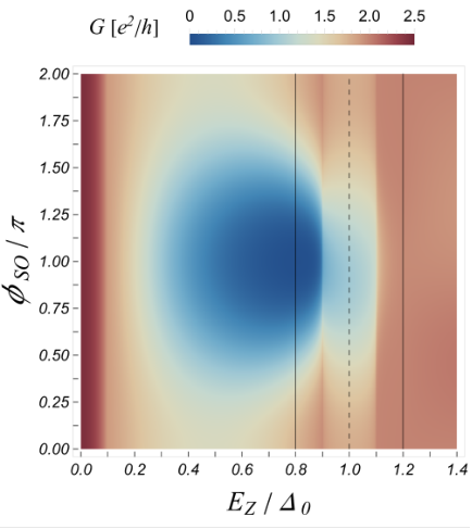
For a Zeeman field smaller than the applied voltage, , the conductance is independent of , as can be inspected by the dark red vertical stripe on the left of Fig.4, where exceeds the single-channel value of a N-S junction. Indeed, at such a weak field, the energy lies above the magnetic gap and two propagating channels are available on the N-side (two incoming electron states and two outgoing hole states). All the spin degrees of freedom are available on both sides of the junction and, as observed above, the misalignment angle simply amounts to a basis rotation, with no physical effects.
However, for , the energy falls inside the magnetic gap, and only a single transport channel remains open, leading to a cusp-like decrease of the conductance. In turn, this leads to a decrease in the available spin degrees of freedom, as observed above, and the dependence on the misalignment angle starts to emerge. It becomes more pronounced for , where the states on both N and S sides contain only half of the complete spin basis. Thus, varying the angle affects the spin-matching between the wavefunctions of the two sides. The vertical line at represents the cut related to Fig.3(c), where the S-side is in the trivial phase: The conductance can be tuned from values as low as up to (in units of ), with varying the SO angle .
Furthermore, a change in the behaviour of the conductance is also observed in the energy Zeeman range . At the two extremal values of such range, the applied voltage exactly matches the bulk superconducting gap . Thus, within such a range of Zeeman field values, the transmission process from the N- to the S-side of the junction opens up. This causes a decrease in the Normal Reflection [ in Eq.(37)] and consequently an increase in the conductance, which becomes less tunable. Notice that the middle value of such a range corresponds to the transition of the S-side from the trivial to topological phase.
Finally, when , transport occurs entirely below the superconducting gap. In particular, the vertical line at represents the cut related to Fig.2(c). As observed above, large values of Zeeman field tend to polarize the states spin, and the tunability of the conductance with respect to the SO angle is almost entirely suppressed.
IV.3 Possible implementations of the setup
Let us now discuss some possible realistic setups where the predicted results about conductance could be observed. NWs based on InSb or InAs characterized by a ballistic transport and a strong SO coupling have been fabricated in a number of experiments [20, 63, 74, 22, 65, 21, 38, 103]. Proximization has been realized by depositing a superconducting film of Al [20, 65, 21], Nb [74, 22] or NbTiN [63, 38, 103] on a NW segment. Focusing e.g. on InSb, the effective electron mass is , and the typical value of SO energy is [63]. With NbTiN films the induced gap parameter is on the order of [63, 103]. The g-factor is [31], and an applied magnetic field of , leads to a Zeeman energy on the order of . The energy ratios used in our plots are compatible with these experimental ranges.
The magnitude of the SO coupling can be controlled via electrolyte gating [55], local top gates [95] or bottom gates patterned beneath the NW [43] or also with gate-all-around geometries, where the NW is fully enclosed by a metallic gate separated by a dielectric layer [81, 87, 89, 102]. Moreover, the large variety of realized gate geometries enable one to control also the direction of the SO field on the N-side of the junction. Side gates, for instance, introduce lateral electric fields that break left–right symmetry and enable rotation of the effective spin–orbit field [82, 42, 26]. Top gates can be combined with bottom or side gates to further enhance tunability. Wrap-around gates, also referred to as -gates, partially surround the nanowire and provide strong capacitive coupling [46, 90, 27, 23, 15]. Furthermore, lateral deposition of the superconducting film proximitizing a NW portion also modifies the SO field direction on the S-side [12, 61]. All these architectures permit precise control of the Rashba coupling, and represent a viable route to observe the predicted tunability effect.
V Conclusions
In this paper, we have investigated how the AR coefficient and the nonlinear conductance in a hybrid N-S junction based on a NW depend on the different orientations and of the SO field on the two sides of the junction. While the energy spectra in the bulk of the two sides are independent of the SO field direction and only depend on the SO magnitude , we have shown that in the hybrid N-S junction SO directions do matter. Indeed, when a magnetic field is applied along the axis of the NW, i.e. perpendicularly to the SO field, the misalignment angle between the two SO field directions and strongly impacts on the Andreev energy-dependence of the reflection coefficient and the nonlinear conductance behavior as a function of the applied voltage bias .
At zero-energy, we have recovered the expected behavior of the AR and linear conductance, which are determined by the topological phase of the S-side of the junction: In the trivial phase one has , whereas in the topological phase one finds and , regardless of the value of the SO misalignment . Such a zero-energy robustness to the SO direction generalizes the results found in N-S junctions in the presence of disorder [3, 99].
However, at finite energy, the SO direction misalignment becomes important. In particular, at finite but low energies , and remain close to the zero energy value and are poorly tunable with , if the S-side is in the topological phase [see Fig.2(b) and (c)]. In striking contrast, when the S-side is in the trivial phase, a wide tunability of and as a function of the SO misalignment is observed at finite energy. As shown in Fig.3(b), the AR coefficient can be tuned from a high value for aligned SO directions (), to an intermediate value (for ), down to a complete AR suppression for a full misalignment (). Similarly, spans from up to (in units of ), with varying the SO angle .
We have pointed out the crucial role played by the magnetic field on determining such a tunability, as highlighted in Fig.4. At too weak magnetic field the conductance is independent of because this is the regime where AR is carried by two independent spin channels and a misalignment of SO directions simply amounts to a spin basis rotation. Similarly, at too large magnetic field, , the tunability with is poor, for the magnetic field spin polarizes the two sides. In contrast, at intermediate Zeeman field values, particularly for , i.e. when the S-side is in the trivial phase, the conductance becomes strongly dependent on the misalignment angle. Finally, we have discussed the implementation in realistic NW-based setup, where SO direction can by now be controlled through various geometrical gating configurations and film deposition designs.
In conclusion, while so far most studies have focussed on controlling electron transport by enhancing the range of the SO coupling magnitude in NWs, our results demonstrate that, even at fixed SO magnitude, the SO direction is a quite efficient knob to electrically tune the AR and the conductance of a NW-based N-S hybrid quantum device. These findings, which could also have potential developments in NW-based Josephson junctions and Andreev spin qubits, suggest that NWs are promising and versatile quantum systems even beyond the search for Majorana quasi-particles.
Acknowledgements.
The authors greatly acknowledge interesting discussions with F. Taddei and A. Braggio. F.D. also acknowledges financial support from the MUR-PRIN 2022—Grant No. 2022B9P8LN-(PE3) Project NEThEQS “Non-equilibrium coherent thermal effects in quantum systems” in PNRR Mission 4-Component 2-Investment 1.1 “Fondo per il Programma Nazionale di Ricerca e Progetti di Rilevante Interesse Nazionale (PRIN)” funded by the Next Generation EU initiative, as well as from the TOPMASQ (”Topological material platform for the implementation of Andreev spin qubit”) project, a Cascade call project (CUP E13C24001560001) financed by the “National Quantum Science & Technology Institute”, PE00000023 (Next Generation EU).Appendix A Eigenstates in the bulk of the N and S sides of the junction
Since in each side the parameters are spatially uniform, one can build up the solution in the hybrid junction by matching the bulk solution in the bulk of the N-side and in the bulk of the S-side. Here below, we specify some details about the bulk eigenstates of the two sides.
A.1 Solutions in the N-side
In the N-side of the junction the superconducting pairing vanishes, . By re-expressing the Nambu spinor field operator in Eq.(7) as , where are the Nambu mode operator and is the entire length of the system, the Hamiltonian (8) acquires a diagonal form in -space, , where
| (39) | |||||||
Here, and
| (40) | |||||
is a -dependent vector determined by the SO field (18) and the magnetic field .
Because the BdG Hamiltonian (39) in the N-side naturally decouples into its two electron and hole blocks, its diagonalization is straightforward and enables one to directly identify, for each of the two excitation bands in Eq.(23), the electron(e) and hole(h) branches.
The electron branch corresponds to the case . It has a spectrum
| (41) |
and its corresponding eigenvectors are
| (42) |
The hole branch corresponds to , has a spectrum
| (43) |
and eigenvectors
| (44) |
In Eqs.(42) and (44), and are the azimuthal and polar angles characterizing the unit vector of in Eq.(40)
| (45) |
and fulfill the relations
| (46) | |||||
| (47) | |||||
| (48) | |||||
where the identities and have been used. By inverting the spectral relations (41) and (43) for the two bands in favor of , one obtains the set of wavevectors at given energy in the N-side, which always come in pairs since are even in k. As a consequence, if the generic solution represents an incoming mode, i.e. , it follows that represents an outgoing mode, i.e. , and viceversa. Thus, in the case of propagating modes, for each pair , we shall provide only the incoming mode solution, labeled by a, while for the evanescent modes we shall write only the physically acceptable in the N-side, i.e. the the solution with negative imaginary part.
For each band () and each branch (), the number and the type (propagating/evanescent) of -solutions of the equation strictly depend on the specific values of the parameters . In particular, depending on the values of and , one can distinguish three different regimes, namely the Rashba dominated regime (), the weak Zeeman regime () and the strong Zeeman regime (). Moreover, within each of these regimes, the chemical potential further determines various ranges for the energy , in which the -wavevectors solving take different expressions. Here below, we shall explicitly provide such expressions in each of the three aforementioned regimes, in terms of the following quantities
| (49) | ||||
| (50) | ||||
| (51) |
A.1.1 Rashba dominated regime ()
Within this regime, the value of the chemical potential identifies various energy ranges. For definiteness, we shall focus on the case
| (52) |
which is the regime that we have considered for the plots shown in the Main Text. Thus, five energy ranges can be distinguished.
Range 1:
| (53) |
where we assign the index “1” to the wavevectors, since in the ranges 4 e 5 (see below), the branch will admit more than two solutions. For the incoming modes the group velocities read
| (54) | ||||
| (55) |
Range 2:
| (56) | ||||
with the group velocities magnitude of the two incoming modes already computed in Eqs. (54)-(55).
Range 3:
| (57) | ||||
where the group velocity for mode is
| (58) |
Range 4:
| (59) |
with the group velocity for incoming mode being
| (60) |
Range 5:
| (61) | ||||
where is defined in Eq.(51). In order to highlight the negative imaginary part, it is possible to rewrite and as
| (62) |
with
| (63) |
Note that two energy threshold values and appear in the above energy ranges. The assumption (52) implies the relation . For chemical potential values outside the range (52), such relation does not hold. Then, the various energy ranges and the expressions of the wavevectors slightly change, although they can be obtained similarly.
A.1.2 Weak Zeeman regime ()
By still assuming that the chemical potential fulfills the condition (52), the weak Zeeman regime identifies the very same five energy ranges as the Rashba dominated regime, where it exhibits the same expressions of the wavevectors, except for the energy range 4, where Eqs.(59) should be now replaced with:
A.1.3 Strong Zeeman regime ()
Also in this regime, the value of the chemical potential determines various energy ranges for the expressions of the wavevectors. Here, we shall assume that the condition
| (65) |
is fulfilled. Then, one has the following five ranges.
A.2 Solutions in the S-side
In the bulk of the proximitized side S, the Hamiltonian is again diagonal in -space, , where, however, the BdG Hamiltonian now contains a finite superconducting pairing and the direction of the SO field (19) differs from the N-side. Explicitly,
| (71) | |||||||
where and
The spectrum of the Hamiltonian Eq.(71) is given by Eq.(24), whereas its eigenstates are given by
| (72) | |||||||
where
| (73) |
and is a normalization constant.
The electron-like or hole-like character of the eigenstates (72) at a given can be attributed through the sign of the quantity defined in Eq.(29).
The electron-like branch corresponds to , and therefore has a spectrum
| (74) |
where are defined in Eq.(24), and corresponding eigenvector
| (75) |
The hole-like branch, corresponding to , has a spectrum
| (76) |
with eigenvectors
| (77) |
Similarly to the approach used for the N-side of the junction, here the wavevectors can be obtained by inverting the spectral relations (74) and (76) in favor of , i.e. by solving . However, differently from the N-side, no analytical approach is viable to obtain the wavevectors for the S-side. Thus, they have been derived via numerical solution, for each energy .
Appendix B Details about the solution of the Scattering Matrix problem
In this Appendix, we provide more technical details about the solution of the Scattering problem outlined in Sec.III.1. At each given energy , and in each side of the interface, one has a number of propagating(pr) channels, where each channel exhibits a mode incoming towards the interface and a mode outgoing from the interface. Thus, in each side, one has unknown amplitudes for propagating modes. Furthermore, each side can also exhibit conjugate pairs of complex modes. However, as mentioned above, only one pair partner describes a physically acceptable mode that does not diverge exponentially, i.e. an evanescent(ev) mode. Let denote the number of evanescent modes in side at the given energy . Since the equation is ultimately a polynomial equation of 8th degree [see Eqs.(23)-(24)], there are always 8 solutions in each side. Thus, the following relation holds
| (78) |
whereas the number of physical mode amplitudes is
| (79) |
Recalling that incoming and outgoing mode amplitudes are labelled by and , respectively, while the evanescent mode amplitudes are labelled by , one can denote by
| (80) |
the vector of the unknown amplitudes on the side . Then, the boundary conditions Eqs.(21)-(22) can compactly be written as
| (81) |
where the matrix and the matrix contain the various waves (propagating or evanescent) in the N- and S-side, respectively, evaluated at .
As a whole, Eq.(81) is a set of 8 linear equations for unknown amplitudes. This implies that one can fix only 8 unknowns in terms of the other variables, which remain undetermined. Exploiting Eqs.(78) and (79), it is straightforward to see that total number of undetermined unknowns
| (82) |
coincides with the total number of propagating channels. Notice also that total number of unknowns that can be determined is . We shall fix the amplitudes of the incoming propagating modes as the undetermined unknowns. Thus, the boundary conditions (81) enable one to express all the amplitudes of the outgoing propagating modes and all the amplitudes of the evanescent modes in terms of the amplitudes of the incoming propagating modes, as follows
| (83) |
where the explicit expression of the matrix can be obtained from numerically solving the linear system (81), at each energy value . In particular, the upper block of is a matrix connecting the outgoing amplitudes to the incoming amplitudes, and is the Scattering matrix appearing in Eq.(31).
References
- [1] (2016) Milestones toward Majorana-based quantum computing. Phys. Rev. X 6, pp. 031016. External Links: Document, Link Cited by: §I.
- [2] (2017) Majorana quasiparticles in condensed matter. Rivista del Nuovo Cimento 40, pp. 523 – 593. External Links: Document, Link Cited by: §I.
- [3] (2011) Quantized conductance at the Majorana phase transition in a disordered superconducting wire. Phys. Rev. Lett. 106, pp. 057001. External Links: Document, Link Cited by: §III.2.1, §III.2.1, §III.2.2, §V.
- [4] (2012) New directions in the pursuit of Majorana fermions in solid state systems. Reports on Progress in Physics 75 (7), pp. 076501. External Links: Document, Link Cited by: §I.
- [5] (1996) Current fluctuations in mesoscopic systems with Andreev scattering. Phys. Rev. B 53, pp. 16390–16402. External Links: Document, Link Cited by: §III.1, §III.1.
- [6] (2026) Enhanced thermoelectricity in nanowires with inhomogeneous helical states. Phys. Rev. Res. 8, pp. 013175. External Links: Document, Link Cited by: §I, §I.
- [7] (2023) Spectroscopy of spin-split Andreev levels in a quantum dot with superconducting leads. Phys. Rev. Lett. 131, pp. 097001. External Links: Document, Link Cited by: §I.
- [8] (1992) Quantum transport in semiconductor-superconductor microjunctions. Phys. Rev. B 46, pp. 12841–12844. External Links: Document, Link Cited by: §III.1, §III.1.
- [9] (2011) Electronic phase coherence in inas nanowires. Nano letters 11, pp. 3550–6. External Links: Document, Link Cited by: §I.
- [10] (1982) Transition from metallic to tunneling regimes in superconducting microconstrictions: excess current, charge imbalance, and supercurrent conversion. Phys. Rev. B 25, pp. 4515–4532. External Links: Document, Link Cited by: §III.1, §III.1.
- [11] (1958) On a new method in the theory of superconductivity. Il Nuovo Cimento 7 (6), pp. 794–805. External Links: ISSN 0029-6341, 1827-6121, Link, Document Cited by: §II.
- [12] (2019) Spin-orbit protection of induced superconductivity in majorana nanowires. Phys. Rev. Lett. 122, pp. 187702. External Links: Document, Link Cited by: §I, §IV.3.
- [13] (2023) Tunable crossed Andreev reflection and elastic cotunneling in hybrid nanowires. Phys. Rev. X 13, pp. 031031. External Links: Document, Link Cited by: §I.
- [14] (2017) Ballistic spin transport in the presence of interfaces with strong spin-orbit coupling. Phys. Rev. B 96, pp. 115445. External Links: Document, Link Cited by: §I, §III.
- [15] (2015) InAs nanowire transistors with multiple, independent wrap-gate segments. Nano Lett. 15 (5), pp. 2836–2843. External Links: Document, Link Cited by: §I, §I, §IV.3.
- [16] (2015) Spin orbit coupling and anomalous Josephson effect in nanowires. Journal of physics. Condensed matter 27, pp. 205301. External Links: Document, Link Cited by: §I.
- [17] (2018) Topological phase detection in Rashba nanowires with a quantum dot. Phys. Rev. B 97, pp. 045404. External Links: Document, Link Cited by: §I.
- [18] (2013) Ballistic InAs nanowire transistors. Nano Letters 13 (2), pp. 555. External Links: Document, Link Cited by: §I, §I.
- [19] (1996) Thermoelectric properties of mesoscopic superconductors. Phys. Rev. B 53, pp. 6605–6612. External Links: Document, Link Cited by: §III.1, §III.1.
- [20] (2012) Zero-bias peaks and splitting in an Al-InAs nanowire topological superconductor as a signature of Majorana fermions. Nat. Phys. 8 (12), pp. 887 – 895. External Links: Document, Link Cited by: §I, §IV.3.
- [21] (2016) Majorana bound state in a coupled quantum-dot hybrid-nanowire system. Science 354 (6319), pp. 1557–1562. External Links: Document, Link Cited by: §I, §IV.3.
- [22] (2012) Anomalous zero-bias conductance peak in a Nb-InSb nanowire-Nb hybrid device. Nano letters 12, pp. 6414. External Links: Document, Link Cited by: §I, §IV.3.
- [23] (2011) Facile fabrication of lateral nanowire wrap-gate devices with improved performance. Applied Physics Letters 99, pp. 173101. External Links: Document, Link Cited by: §I, §I, §IV.3.
- [24] (2009) Quantum interference effects in InAs semiconductor nanowires. Journal of the Korean Physical Society 54 (1), pp. 135 – 139. External Links: Link Cited by: §I.
- [25] (2018) Magnetic field effects on a nanowire with inhomogeneous rashba spin-orbit coupling: spin properties at equilibrium. Phys. Rev. B 98, pp. 045436. External Links: Document, Link Cited by: §I, §III, §IV.1.
- [26] (2019) Side-gated, enhancement mode, inas nanowire double quantum dot devices – toward controlling transverse electric fields in spin-transport measurements. Nanotechnology 30, pp. 144002. External Links: Document, Link Cited by: §I, §I, §IV.3.
- [27] (2010) Vertical InAs nanowire wrap gate transistors with GHz and ghz. Nano letters 10, pp. 809–12. External Links: Document Cited by: §I, §I, §IV.3.
- [28] (2021) Heat transport control and thermal characterization of low-dimensional materials: a review. Nanomaterials 11 (1), pp. 175. External Links: Document, Link Cited by: §I.
- [29] (2010) Spin-orbit coupling and phase coherence in InAs nanowires. Physical Review B 82 (23). External Links: Link Cited by: §I.
- [30] (2017) Observation of conductance quantization in InSb nanowire networks. Nano Letters 17 (11), pp. 6511 – 6515. External Links: Link Cited by: §I.
- [31] (2015) Formation of long single quantum dots in high quality InSb nanowires grown by molecular beam epitaxy. Nanoscale 7, pp. 14822–14828. External Links: Document, Link Cited by: §I, §IV.3.
- [32] (2024) Opportunities for the direct manipulation of a phase-driven Andreev spin qubit. Phys. Rev. B 109, pp. 184515. External Links: Document, Link Cited by: §I.
- [33] (2025) Long-range crossed Andreev reflection in a topological insulator nanowire proximitized by a superconductor. Nature Physics 21, pp. 708–715. External Links: Document, Link Cited by: §I.
- [34] (2020) Quantum-confinement-enhanced thermoelectric properties in modulation-doped GaAs–AlGaAs core–shell nanowires. Adv. Mater. 32 (4), pp. 1905458. External Links: Document, Link Cited by: §I.
- [35] (2018) Superconductivity of metals and alloys. Advanced book classics, CRC Press, Taylor & Francis Group, Boca Raton. External Links: ISBN 978-0-7382-0101-6, Document Cited by: §II.
- [36] (2022) Electron transport in quantum channels with spin-orbit interaction: effects of the sign of the Rashba coupling and applications to nanowires. New Journal of Physics 24, pp. 093025. External Links: Document, Link Cited by: §I.
- [37] (2022) The Dirac paradox in 1+1 dimensions and its realization with spin-orbit coupled nanowires. New Journal of Physics 24, pp. 053045. External Links: Document, Link Cited by: §I.
- [38] (2017) Hard superconducting gap in InSb nanowires. Nano letters 17, pp. 2690. External Links: Document, Link Cited by: §I, §IV.3.
- [39] (2021) Coherent manipulation of an Andreev spin qubit. Science 373 (6553), pp. 430–433. External Links: Document, Link Cited by: §I.
- [40] (2020) Continuous monitoring of a trapped superconducting spin. Nature Physics 16, pp. 1–5. External Links: Document Cited by: §I.
- [41] (2016) Ballistic transport and exchange interaction in InAs nanowire quantum point contacts. Nano Letters 16 (5), pp. 3116. External Links: Document, Link Cited by: §I.
- [42] (2018) Vectorial control of the spin–orbit interaction in suspended inas nanowires. Nano Letters 19 (2), pp. 652–657. External Links: ISSN 1530-6984, Document, Link Cited by: §I, §I, §IV.3.
- [43] (2017) Conductance through a helical state in an indium antimonide nanowire. Nature Communications 8, pp. 478. External Links: Document, Link Cited by: §I, §I, §IV.3.
- [44] (2016) Conductance quantization at zero magnetic field in InSb nanowires. Nano Letters 16 (6), pp. 3482 – 3486. External Links: Link Cited by: §I.
- [45] (2013) Measurement of thermoelectric properties of single semiconductor nanowires. Journal of Electronic Materials 42 (7), pp. 2409 – 2414. External Links: Document, Link Cited by: §I.
- [46] (2006) Fabrication and device characterization of omega-shaped-gate ZnO nanowire field-effect transistors. Nano Letters 6 (7), pp. 1454–1458. External Links: ISSN 1530-6984, Document, Link Cited by: §I, §I, §IV.3.
- [47] (1999) Superconductivity. Cambridge University Press, Cambridge. External Links: ISBN 978-1-139-17109-0, Document Cited by: §II.
- [48] (2015) Fermionic and Majorana bound states in hybrid nanowires with non-uniform spin-orbit interaction. The European Physical Journal B 88, pp. 62. External Links: Document, Link Cited by: §I.
- [49] (2018) Direct Rashba spin-orbit interaction in Si and Ge nanowires with different growth directions. Phys. Rev. B 97, pp. 235422. External Links: Document, Link Cited by: §I.
- [50] (1993) Multi-probe conductance formulae for mesoscopic superconductors. Journal of Physics: Condensed Matter 5 (25), pp. 4187. External Links: Document, Link Cited by: §III.1, §III.1.
- [51] (1998) Phase-coherent transport in hybrid superconducting nanostructures. Journal of Physics: Condensed Matter 10 (5), pp. 901. External Links: Document, Link Cited by: §III.1, §III.1.
- [52] (1991) Generalized Landauer formulae for quasi-particle transport in disordered superconductors. J. Phys. Condensed Matter 3 (34), pp. 6579. External Links: Document, Link Cited by: §III.1, §III.1.
- [53] (1993) Quantum interference from superconducting islands in a mesoscopic solid. Journal of Physics: Condensed Matter 5 (6), pp. 707. External Links: Document, Link Cited by: §III.1, §III.1.
- [54] (2017) Ballistic transport and quantum interference in InSb nanowire devices. Chinese Physics B 26 (2). External Links: Link Cited by: §I.
- [55] (2012) Strong tuning of Rashba spin-orbit interaction in single InAs nanowires. Nano letters 12, pp. 3263–7. External Links: Document, Link Cited by: §I, §I, §IV.3.
- [56] (2007) From Coulomb blockade to the Kondo regime in a Rashba dot. Phys. Rev. B 76, pp. 035307. External Links: Document, Link Cited by: §I, §III.
- [57] (2025) Andreev spin relaxation time in a shadow-evaporated InAs weak link. Phys. Rev. Appl. 24, pp. 024046. External Links: Document, Link Cited by: §I.
- [58] (2025) Kramers-protected hardware-efficient error correction with Andreev spin qubits. Phys. Rev. Lett. 135, pp. 210602. External Links: Document, Link Cited by: §I.
- [59] (2010) Majorana fermions and a topological phase transition in semiconductor-superconductor heterostructures. Phys. Rev. Lett. 105, pp. 077001. External Links: Document, Link Cited by: §I, §II.2, §II.2.
- [60] (2024) Nonlocal thermoelectricity in quantum wires as a signature of Bogoliubov-Fermi points. Phys. Rev. B 110, pp. 075415. External Links: Document, Link Cited by: §I.
- [61] (2024) Gate-tunable Josephson diode. Phys. Rev. Appl. 22, pp. 054034. External Links: Document, Link Cited by: §I, §IV.3.
- [62] (2021) Circuit-QED with phase-biased Josephson weak links. Phys. Rev. Res. 3, pp. 013036. External Links: Document, Link Cited by: §I.
- [63] (2012) Signatures of Majorana fermions in hybrid superconductor–semiconductor nanowire devices. Science 336 (6084), pp. 1003–1007. External Links: Document, Link, ISSN 1095-9203 Cited by: §I, §IV.3.
- [64] (2016) Anomalous josephson effect in semiconducting nanowires as a signature of the topologically nontrivial phase. Phys. Rev. B 93, pp. 174502. External Links: Document, Link Cited by: §I, §II.2, §IV.1.
- [65] (2011) Supercurrent and multiple Andreev reflections in an InSb nanowire josephson junction. Nano letters 12, pp. 228–33. External Links: Document, Link Cited by: §I, §IV.3.
- [66] (2010) Helical liquids and Majorana bound states in quantum wires. Phys. Rev. Lett. 105, pp. 177002. External Links: Document, Link Cited by: §I, §II.2, §II.2.
- [67] (2017) Andreev spin qubits in multichannel Rashba nanowires. Phys. Rev. B 96, pp. 125416. External Links: Document, Link Cited by: §I.
- [68] (2023) Direct manipulation of a superconducting spin qubit strongly coupled to a transmon qubit. Nature Physics 19, pp. 1110. External Links: Document Cited by: §I.
- [69] (2025) Blueprint for all-to-all-connected superconducting spin qubits. PRX Quantum 6, pp. 010308. External Links: Document, Link Cited by: §I.
- [70] (2024) Strong tunable coupling between two distant superconducting spin qubits. Nature Physics 20 (7), pp. 1158–1163. External Links: Document Cited by: §I.
- [71] (2020) From Andreev to Majorana bound states in hybrid superconductor–semiconductor nanowires. Nat. Rev. Phys. 2 (10), pp. 575–594. External Links: Document, Link, ISSN 2522-5820 Cited by: §I.
- [72] (2013) Electrical control of single hole spins in nanowire quantum dots. Nature Nanotechnology 8 (3), pp. 170 – 174. External Links: Link Cited by: §I.
- [73] (2018) Zero-energy Andreev bound states from quantum dots in proximitized Rashba nanowires. Phys. Rev. B 98, pp. 245407. External Links: Document, Link Cited by: §I.
- [74] (2012) The fractional a.c. Josephson effect in a semiconductor-superconductor nanowire as a signature of Majorana particles. Nature Physics 8, pp. 795–799. External Links: Document, Link Cited by: §I, §IV.3.
- [75] (2020) Confinement versus interface bound states in spin-orbit coupled nanowires. The European Physical Journal Plus 135, pp. 597. External Links: Document, Link Cited by: §I, §III.
- [76] (2020) Majorana-like localized spin density without bound states in topologically trivial spin-orbit coupled nanowires. Phys. Rev. B 101, pp. 195421. External Links: Document, Link Cited by: §I, §II.2, §III.
- [77] (2013) Effect of gate-driven spin resonance on the conductance through a one-dimensional quantum wire. Phys. Rev. B 88, pp. 115302. External Links: Document, Link Cited by: §I, §III.
- [78] (2013) Multiple Andreev reflection and critical current in topological superconducting nanowire junctions. New Journal of Physics 15 (7), pp. 075019. External Links: Document, Link Cited by: §I.
- [79] (2008) Strongly modulated transmission of a spin-split quantum wire with local Rashba interaction. Phys. Rev. B 77, pp. 035315. External Links: Document, Link Cited by: §I, §III.
- [80] (2006) Fano-Rashba effect in a quantum wire. Phys. Rev. B 74, pp. 153313. External Links: Document, Link Cited by: §I, §III.
- [81] (2013) Encapsulated gate-all-around InAs nanowire field-effect transistors. Applied Physics Letters 103, pp. 213502. External Links: Document, Link Cited by: §I, §I, §IV.3.
- [82] (2016) Electrical tuning of Rashba spin-orbit interaction in multigated InAs nanowires. Phys. Rev. B 94, pp. 035444. External Links: Document, Link Cited by: §I, §I, §IV.3.
- [83] (2013) Performance comparison of InAs, InSb, and GaSb n-channel nanowire metal-oxide-semiconductor field-effect transistors in the ballistic transport limit. Applied Physics Express 6 (3). External Links: Link Cited by: §I.
- [84] (2018) Building topological quantum circuits: majorana nanowire junctions. Phys. Rev. B 97, pp. 045410. External Links: Document, Link Cited by: §I, §I.
- [85] (2003) Antisymmetric spin filtering in one-dimensional electron systems with uniform spin-orbit coupling. Phys. Rev. Lett. 90, pp. 256601. External Links: Document, Link Cited by: §II.2, §IV.1.
- [86] (2017) Spin and charge signatures of topological superconductivity in Rashba nanowires. Phys. Rev. B 96, pp. 041401(R). External Links: Document, Link Cited by: §I.
- [87] (2017) Highly gate-tuneable Rashba spin-orbit interaction in a gate-all-around InAs nanowire metal-oxide-semiconductor field-effect transistor. Sci. Rep. 7 (1), pp. 930. External Links: Document, Link, ISSN 2045-2322 Cited by: §I, §I, §IV.3.
- [88] (2017) Highly gate-tuneable Rashba spin-orbit interaction in a gate-all-around InAs nanowire metal-oxide-semiconductor field-effect transistor. Scientific Reports 7 (1). External Links: Link Cited by: §I.
- [89] (2021) Electrical tuning of the spin–orbit interaction in nanowire by transparent ZnO gate grown by atomic layer deposition. Appl. Phys. Lett. 119 (1), pp. 013102. External Links: ISSN 0003-6951, Document, Link Cited by: §I, §I, §IV.3.
- [90] (2008) Vertical enhancement-mode InAs nanowire field-effect transistor with 50-nm wrap gate. IEEE Electron Device Letters 29, pp. 206–208. External Links: Document, Link Cited by: §I, §I, §IV.3.
- [91] (2019) Spin-orbit splitting of Andreev states revealed by microwave spectroscopy. Phys. Rev. X 9, pp. 011010. External Links: Document, Link Cited by: §I.
- [92] (2008) Spin dynamics in InAs nanowire quantum dots coupled to a transmission line. Physical Review B - Condensed Matter and Materials Physics 77 (4). External Links: Link Cited by: §I.
- [93] (2013) Fast spin-orbit qubit in an indium antimonide nanowire. Physical Review Letters 110 (6). External Links: Link Cited by: §I.
- [94] (2009) Selective excitation and detection of spin states in a single nanowire quantum dot. Nano Letters 9 (5), pp. 1989 – 1993. External Links: Link Cited by: §I.
- [95] (2015) Spin-orbit interaction in InSb nanowires. Phys. Rev. B 91, pp. 201413(R). External Links: Document, Link Cited by: §I, §I, §IV.3.
- [96] (2012) Room-temperature terahertz detectors based on semiconductor nanowire field-effect transistors. Nano Letters 12 (1), pp. 96 – 101. External Links: Document, Link Cited by: §I.
- [97] (2015) Phase-coherent transport and spin relaxation in InAs nanowires grown by molecule beam epitaxy. Applied Physics Letters 106, pp. 173105. External Links: Document, Link Cited by: §I.
- [98] (2012) Quantized conductance in an InSb nanowire. Nano letters 13, pp. 387. External Links: Document, Link Cited by: §I.
- [99] (2011) Quantum point contact as a probe of a topological superconductor. New Journal of Physics 13 (5), pp. 053016. External Links: Document, Link Cited by: §III.2.1, §III.2.1, §V.
- [100] (2018) Tuning rashba spin-orbit coupling in homogeneous semiconductor nanowires. Phys. Rev. B 97, pp. 165401. External Links: Document, Link Cited by: §I.
- [101] (2012) Phase coherent transport in insb nanowires. Applied Physics Letters 101, pp. 082103. External Links: Document, Link Cited by: §I.
- [102] (2021) Tellurium nanowire gate-all-around MOSFETs for sub‑5 nm applications. ACS Applied Materials & Interfaces 13 (2), pp. 3387–3396. External Links: ISSN 1944-8244, Document, Link Cited by: §I, §I, §IV.3.
- [103] (2018) Ballistic Majorana nanowire devices. Nature Nanotechnology 13, pp. 192–197. External Links: Document, Link Cited by: §I, §I, §IV.3.
- [104] (2006) Direct observation of ballistic and drift carrier transport regimes in InAs nanowires. Applied Physics Letters 89 (5), pp. 053113. External Links: Document, Link Cited by: §I.