Aperiodic temporal modulation for distortionless broadband impedance matching beyond the Bode-Fano limit
Abstract
The Bode–Fano bound sets a fundamental trade-off between bandwidth and reflection in passive, linear, time-invariant matching networks. We show that an aperiodically time-modulated reactive element can emulate the non-Foster response required to match a prescribed pulse, achieving reflectionless, nearly distortionless energy transfer beyond the Bode–Fano limit. The approach introduces a new constraint: a minimum dc bias that scales with pulse bandwidth, derived from the requirement that the modulated capacitance remain positive at all times. This modulation-bias bound replaces the classical bandwidth-reflection trade-off with a bandwidth-energy trade-off. A realistic circuit simulation confirms broadband matching with preserved waveform fidelity, demonstrating that the scheme is physically realizable and not merely a mathematical circumvention.
The Bode–Fano (BF) bound 1; 3 establishes a fundamental limit on broadband impedance matching in electromagnetic engineering. It defines an inherent trade-off between bandwidth and matching efficiency: the bandwidth over which high-efficiency transfer of energy to a given load is maximized and reflections are minimized is fundamentally limited. This limitation is particularly significant for electrically small devices, as these tend to behave as highly reactive loads.
Importantly, two other fundamental electromagnetic limits—Chu’s limit for small antennas 38; 2 and Rozanov’s bound for thin absorbers 26—can ultimately be treated as impedance-matching problems, see, e.g., Refs. 22; 18; 4. Therefore, the BF bound serves as an essential reference point for designing compact devices in fields such as medical equipment, portable wireless devices, communication systems, and sensors, where space constraints make broadband matching challenging.
To circumvent the BF bound, approaches that deliberately violate its underlying assumptions—linearity, passivity, and time invariance—and enable broadband matching have been actively pursued. Early efforts primarily focused on breaking the passivity assumption by using non-Foster (active) elements 9; 40; 16. However, non-Foster matching networks are well known to suffer from stability issues and to degrade the signal-to-noise ratio (SNR) 36; 10; 33. More recently, renewed interest in time-varying media has opened the door to new wave phenomena, see, e.g., Refs. 6; 20; 25; 13; 17; 21; 11; 27; 28, and provided an alternative route to broadband matching by violating the time-invariance assumption. Time-modulation approaches can be divided into two categories, depending on whether they use periodic or non-periodic forms of modulation. Periodic modulation allows one to design matching networks that are independent of the input signals 15; 5. However, they need to access regimes of parametric gain, otherwise such networks follow bounds similar to the BF bound 35. Parametric gain is more controllable than other active devices, but can still lead to instabilities. Aperiodic forms of temporal modulation can expand the return loss bandwidth beyond the BF bound without the problem of instabilities 34; 39, but they are not signal agnostic, i.e., they need to be timed with the specific signal they need to impedance match. In addition, existing approaches are based on abrupt switching, and generally introduce distortion to the signal transmitted to the load.
In a different context, it has been shown that time modulation can be used to transform the response of a circuit for prescribed input signals 8; 24, enabling also non-Foster responses. This approach also requires time synchronization between the modulation and the incoming signals. Here, we use aperiodic modulation to realize effective non-Foster responses for broadband matching of highly reactive loads. In addition to completely suppressing reflections, this approach minimizes the temporal distortion of the signal at the load, thereby preserving the waveform of the pulse to be transmitted or radiated. Similarly to other approaches that transform the circuit response with time modulation 8; 30; 24, we need to bias with a nonzero static voltage the modulation waveform, in order to avoid nonphysical values in the modulated components. To understand the implications of this requirement, we derive bounds on the minimum required static bias versus the pulse bandwidth and energy for arbitrary pulse profiles. We validate the proposed matching approach in a realistic circuit implementation and transient nonlinear circuit simulations, showing that it can indeed surpass the BF bound.
Aperiodically Time-Modulated Matching Network.–We begin by considering the canonical architecture modeling an impedance matching problem: a matching network between a transmission line and a load (Fig. 1). In the proposed scheme, the matching network is an aperiodically time modulated capacitor . The load is assumed to be inductive, a resistor in series with an inductor , modeling, for example, an electrically small loop antenna. Transformers can equalize the real part of the load to the transmission-line characteristic impedance over a relatively broad bandwidth. Thus, we assume . The circuit is excited by a voltage pulse that propagates along the line towards the load, and the variable capacitor is connected to a DC source . Similarly to other approaches for the implementation of arbitrary circuit responses using time modulation 8; 30; 24; 31, a DC bias is necessary to avoid singularities or negative values in the time-varying capacitor.
By enforcing zero reflections and assuming that the voltage across the resistor is the same as the input pulse, i.e., , Kirchhoff’s voltage law (KVL) yields , with and denoting the voltage across the capacitor and the inductor, respectively. By combining the previous equation with the capacitor - relation, we obtain the required temporal variation of the capacitance to fully transmit to the resistor load without distortion 29,
| (1) |
with denoting the initial value of the capacitance. Eq. (1) can be written as , where is the current flowing through the circuit and is the alternating component of the capacitor voltage. This is the constitutive relation of a negative inductor showing that the time-varying capacitor realizes such an inductance for the specified incident pulse.
As an illustrative example, we consider a modulated Gaussian pulse , where , , , and denote the pulse amplitude, temporal center, temporal width, and carrier frequency, respectively. Replacing into Eq. (1), an analytical form for can be obtained 29. Figs. 2(a) and (b) show the temporal profile of for and , respectively. As increases, the bandwidth of decreases and, as expected, a smaller excursion of is required to achieve matching. To validate the matching capabilities of these capacitance profiles, the architecture of Fig. 1 is implemented in Keysight ADS 12, with the time-varying capacitor realized through a linear symbolically defined device. Figs. 2(c) and (d) show the voltage across the load resistor for and , respectively. In each plot, the input pulse and the load voltage for matching with a linear time-invariant (LTI) capacitor equal to are also reported for comparison. The parameters of the load are selected to give a characteristic decay time ns, significantly larger than the characteristic time of the pulse, thus representing a remarkably challenging matching scenario. In this case, the LTI configuration leads to strong reflections and a pronounced ringing response in the load voltage. In contrast, when the capacitor is modulated according to Eq. (1), the voltage across the load closely reproduces the input pulse, demonstrating distortionless matching.

The approach described above works for pulses of arbitrarily large bandwidths. However, as we will show next, a larger bandwidth requires the use of a larger to avoid nonphysical values for , such as negative values or infinities. To ensure that remains finite and strictly positive for any , must be chosen to prevent (i) singularities and (ii) sign changes in Eq. (1). These requirements yield two admissible branches for , a positive and a negative branch, depending on whether the numerator and denominator in Eq. (1) are both positive or negative, respectively. The positive branch is defined by , where and are the lower limits on for the numerator and denominator to be positive, respectively. The negative branch is defined by , where and are the upper limits on for the numerator and denominator to be negative, respectively.

To better understand the effect of the load and pulse characteristics on these limits, we derive for the modulated Gaussian pulse introduced earlier. For this pulse, and can be evaluated analytically 29 and are plotted versus versus in Fig. 3(a). These results are derived for fixed load parameters and a fixed energy, , for the pulse. The green regions in Fig. 3 represent the allowed values of . As increases, and decrease, showing that the required decreases as the pulse bandwidth decreases. In the limiting case of large (narrowband pulses), and . This result shows that, for large , decreases as . A similar behavior is observed for the negative branch [Fig. 3(b)]. In the opposite limiting case of small (wide bandwidth), and . The latter expression is strongly dominant, increasing as decreases, while exhibits the opposite trend [Fig. 3(a)]. A similar behavior is observed for the negative branch, with being strongly dominant [Fig. 3(b)]. In either case, the minimum required scales as . From Figs. 3(a) and (b), we also observe that, for a given , the negative branch yields lower absolute DC bias voltages and is therefore preferable for designs targeting the minimum . Finally, comparing the temporal profiles of obtained from Eq. (1) for different and the same shows that selecting close to the limits leads to larger peak excursions for .
The bounds derived above show that for . For pulses of fixed energy, this is a result of the fact that, in the limit , the pulse amplitude goes to zero, essentially implying no input signal. A more realistic scenario in the limit is for pulses of constant amplitude , which become continuous signals in the limit . In such a case, it can be shown that , with a constant that depends only on the load 29. This seems to suggest that a nonzero is necessary even for continuous signals, contrary to what is expected from conventional matching theory, where a continuous signal can be perfectly matched to a reactive load by simply selecting to resonate with the load at the frequency of the signal. The resolution to this paradox comes from the fact that is derived under the very strict condition of zero reflection. As we show in 29, in the limit , and reflections stay low for a wide range of values that can be different from the used in the evaluation of through Eq. (1).
The previous analysis can be extended to arbitrary pulses by using Bernstein’s inequality 14; 23. To this end, we consider pulses with finite energy () and finite support . Under these assumptions, Bernstein’s inequality combined with Fourier inversion and the Cauchy–Schwarz inequality 14 allows us to derive a sufficient condition on the minimum biasing voltage as
| (2a) | ||||||
| (2b) | ||||||
where is the bandwidth and the center frequency of the pulse. The mathematical details of this derivation are provided in 29. The bound predicts the same admissible regions for positive and negative , which is expected from the waveform independence of the bound. The admissible threshold exhibits the same scaling with respect to and as for the case of the modulated Gaussian pulse. In the limiting case of narrow bandwidth (), , and Eqs. (2a) and (2b) reduce to for and for , respectively. Consistent with the behavior observed for the modulated Gaussian pulse, the bound monotonically decrease with decreasing bandwidth .
In the opposite limit of wide bandwidth, and , and Eqs. (2a) and (2b) reduce to for and for . This scaling behavior is the same as for the modulated Gaussian pulse (Fig. 3). This result shows that the proposed approach allows the matching of arbitrarily broadband pulses at the expense of a larger .

Modulation Energy.–In lossless linear time-invariant (LTI) matching networks, energy transfer from the source to the load is maximized by minimizing the reflection coefficient. In contrast, in time-varying matching networks, there can be energy exchange between the modulation source and the system. As a result, even in the absence of reflection, the energy delivered to the load may differ from the incident energy, as part of it can be exchanged with the modulation source. For the circuit analyzed here, the net modulation energy over the entire process is , where and are the capacitor charges before and after the transmission of the incident pulse to the load, respectively. This expression for is a direct consequence of energy conservation and, therefore, does not depend on the shape of the incoming pulse. Instead, it depends only on the difference of the capacitor energy before and after the pulse, which is given by one half the product of with . By charge conservation, this variation is related to the current of the incoming pulse as . Thus, when the incoming pulse carries zero net charge (), the modulation energy vanishes. This is the case of the modulated Gaussian pulse considered earlier. As shown in 29, during the transient, the capacitor charge increases and decreases by equal amounts relative to its initial value , resulting in . The corresponding temporal evolution of the modulation energy indicates that the modulation source injects and extracts the same amount of energy from the system 29, yielding . In contrast, if the incoming pulse carries a nonzero net charge, such as a Gaussian pulse, , leading to a nonzero modulation energy. This energy exchange between the system and the modulation source arises from the interplay between the DC bias and the incoming pulse. Specifically, a positive (negative) net flow of charge leads to an increase (decrease) of stored charge in the capacitor, and to energy extraction (injection) by the modulation source 29.
Proposed Practical Implementation.–To validate the main features of the proposed time-varying matching scheme, we consider the realistic implementation in Fig. 4(a), consisting of a differential circuit in which the time-varying capacitor is realized by using a Wheatstone bridge of four varactors. The initial equivalent capacitance is set by the bias voltage and subsequently modulated in time through the control signal . The input signal is equal to the modulated gaussian pulse introduced earlier and models the forward-propagating pulse in the transmission line model of Fig. 1. The circuit is analyzed by using a commercial transient circuit simulator. The nonlinear model of the varactor (inverse square root model of an inversely biased diode) is used to determine the modulation signal that produces the required capacitance profile . Figs. 4(b) and (c) show the voltage across the load resistor, , obtained from the nonlinear transient circuit simulations for two different values of . An excellent agreement with the input pulse can be observed, demonstrating the capability of the proposed approach to achieve matching without distorting the signal.
On the other hand, matching with a time-invariant capacitor leads to a long damping time, strong reflections and a long ringing response in the voltage across the resistor [continuous solid black line in Figs. 4(b) and (c)].
Further insight into the spectral characteristics of the output signal and the ability of the proposed approach to surpass the BF bound can be gained by examining the energy spectrum of the output voltage. In Fig. 4(d), the gray-shaded region denoted as the BF region represents the area where an output pulse is bound to reside for any low-ripple passive time-invariant matching network as predicted from the Bode–Fano bound. The input voltage spectrum is also shown, together with the output spectrum of matching with a time-invariant capacitor and the output spectrum for the proposed time-modulated matching network. The unmodulated response, as expected, lies within the BF region, whereas the time-modulated response extends to a large degree beyond the bound, demonstrating a significant enhancement of the matching bandwidth beyond the BF bound.
Conclusion.–In this Letter, we introduced a time-modulated matching framework that enables distortionless broadband impedance matching beyond the limitations imposed by the BF bound. By employing aperiodic temporal modulation of reactive elements, the proposed approach enables broadband, reflectionless energy transfer while preserving the temporal profile of the incident pulse. Our analysis establishes a lower bound on an electric dc biasing required to ensure physically realizable modulation and provides an in-depth formulation for the modulation energy that applies to a large variety of pulses. We validated our results through a realistic circuit implementation, showing that the resulting output spectra extend beyond the BF bound. The approach requires prior knowledge of the incident waveform and synchronization between the waveform and the prescribed temporal modulation; however, the analysis in 29 shows that the normalized reflected energy is first-order insensitive to small synchronization errors. Because the RF and modulation-control paths are, in principle, independently generated, synchronization need not rely on feedback and may instead be established using a common timing reference. This differs from many non-Foster implementations, in which the synthesized impedance is realized through an active feedback network and is therefore directly subject to loop-stability constraints. These findings open new opportunities for broadband impedance matching in a wide range of electromagnetic systems, including antennas, RF front ends, and photonic platforms. More broadly, this framework offers a promising pathway to revisit and potentially overcome classical performance limits in electromagnetic systems.
Acknowledgments.– N.E. and A.A. acknowledge partial support from the Simons Foundation/Collaboration on Symmetry-Driven Extreme Wave Phenomena (Grant No. SFI-MPS-EWP-00008530-04). A.A. and D.L.S. acknowledge support from the Air Force Office of Scientific Research.
∗Corresponding author.
mencagli@udel.edu
References
- Network analysis and feedback amplifier design. Van Nostrand, New York. Cited by: Aperiodic temporal modulation for distortionless broadband impedance matching beyond the Bode-Fano limit.
- Physical limitations on omni-directional antennas. Journal of Applied Physics 19 (12), pp. 1163–1175. Cited by: Aperiodic temporal modulation for distortionless broadband impedance matching beyond the Bode-Fano limit.
- [3] Theoretical limitations on the broadband matching of arbitrary impedances. Note: Technical Report No. 41, Research Laboratory of Electronics, MIT, 1948 Cited by: Aperiodic temporal modulation for distortionless broadband impedance matching beyond the Bode-Fano limit.
- Sum rule bounds beyond rozanov criterion in linear and time-invariant thin absorbers. Phys. Rev. B 108, pp. 014308. Cited by: Aperiodic temporal modulation for distortionless broadband impedance matching beyond the Bode-Fano limit.
- Space–time modulation of a multimode electrically small antenna for increased matching and efficiency bandwidths. IEEE Transactions on Antennas and Propagation 73 (3), pp. 1308–1320. Cited by: Aperiodic temporal modulation for distortionless broadband impedance matching beyond the Bode-Fano limit.
- Photonics of time-varying media. Advanced Photonics 4 (1), pp. 014002. Cited by: Aperiodic temporal modulation for distortionless broadband impedance matching beyond the Bode-Fano limit.
- First-principles analysis of energy exchange in time-varying capacitors for energy trapping applications. IEEE Access 11 (), pp. 71494–71502. Cited by: Aperiodic temporal modulation for distortionless broadband impedance matching beyond the Bode-Fano limit, Aperiodic temporal modulation for distortionless broadband impedance matching beyond the Bode-Fano limit.
- Time-varying route to non-foster elements. In 2020 Fourteenth International Congress on Artificial Materials for Novel Wave Phenomena (Metamaterials), Vol. , pp. 108–109. Cited by: Aperiodic temporal modulation for distortionless broadband impedance matching beyond the Bode-Fano limit, Aperiodic temporal modulation for distortionless broadband impedance matching beyond the Bode-Fano limit.
- Negative capacitor paves the way to ultra-broadband metamaterials. Appl. Phys. Lett. 99 (25), pp. 254103. Cited by: Aperiodic temporal modulation for distortionless broadband impedance matching beyond the Bode-Fano limit.
- Gain and noise analysis of non-foster matched antennas. IEEE Trans. Antennas Propag. 64 (12), pp. 4993–5004. Cited by: Aperiodic temporal modulation for distortionless broadband impedance matching beyond the Bode-Fano limit.
- Time-varying components for enhancing wireless transfer of power and information. Phys. Rev. Appl. 16, pp. 014017. Cited by: Aperiodic temporal modulation for distortionless broadband impedance matching beyond the Bode-Fano limit.
- Advanced design system (ads). Keysight Technologies. Note: Electronic design automation software External Links: Link Cited by: Aperiodic temporal modulation for distortionless broadband impedance matching beyond the Bode-Fano limit.
- Time-varying media, dispersion, and the principle of causality [invited]. Optical Materials Express 14 (5), pp. 1222–1236. Cited by: Aperiodic temporal modulation for distortionless broadband impedance matching beyond the Bode-Fano limit.
- A foundation in digital communication. Cambridge University Press, Cambridge, UK. Cited by: Aperiodic temporal modulation for distortionless broadband impedance matching beyond the Bode-Fano limit.
- Beyond chu’s limit with floquet impedance matching. Phys. Rev. Lett. 123, pp. 164102. Cited by: Aperiodic temporal modulation for distortionless broadband impedance matching beyond the Bode-Fano limit.
- Broadband parametric impedance matching for small antennas using the bode-fano limit: improving on chu’s limit for loaded small antennas. IEEE Antennas and Propagation Magazine 64 (5), pp. 55–68. Cited by: Aperiodic temporal modulation for distortionless broadband impedance matching beyond the Bode-Fano limit.
- Topological aspects of photonic time crystals. Optica 5 (11), pp. 1390–1395. Cited by: Aperiodic temporal modulation for distortionless broadband impedance matching beyond the Bode-Fano limit.
- Fundamental limits, bandwidth, and information rate of electrically small antennas: increasing the throughput of an antenna without violating the thermodynamic q-factor. IEEE Antennas Propag. Mag. 61 (3), pp. 14–26. Cited by: Aperiodic temporal modulation for distortionless broadband impedance matching beyond the Bode-Fano limit.
- Static-to-dynamic field conversion with time-varying media. Phys. Rev. B 105, pp. 144301. Cited by: Aperiodic temporal modulation for distortionless broadband impedance matching beyond the Bode-Fano limit.
- Tutorial on the conservation of momentum in photonic time-varying media [invited]. Optical Materials Express 13 (6), pp. 1598–1608. Cited by: Aperiodic temporal modulation for distortionless broadband impedance matching beyond the Bode-Fano limit.
- Antireflection temporal coatings. Optica 7 (4), pp. 323–331. Cited by: Aperiodic temporal modulation for distortionless broadband impedance matching beyond the Bode-Fano limit.
- Fundamental efficiency limits for small metallic antennas. IEEE Transactions on Antennas and Propagation 65 (4), pp. 1642–1650. Cited by: Aperiodic temporal modulation for distortionless broadband impedance matching beyond the Bode-Fano limit.
- Introduction to fourier analysis and wavelets. Brooks/Cole, Pacific Grove, CA. Cited by: Aperiodic temporal modulation for distortionless broadband impedance matching beyond the Bode-Fano limit.
- Time-modulated circuits and metasurfaces for emulating arbitrary transfer functions. Phys. Rev. Appl. 20, pp. 014041. Cited by: Aperiodic temporal modulation for distortionless broadband impedance matching beyond the Bode-Fano limit, Aperiodic temporal modulation for distortionless broadband impedance matching beyond the Bode-Fano limit.
- A tutorial on the basics of time-varying electromagnetic systems and circuits: historic overview and basic concepts of time-modulation. IEEE Antennas and Propagation Magazine 65 (4), pp. 10–20. Cited by: Aperiodic temporal modulation for distortionless broadband impedance matching beyond the Bode-Fano limit.
- Ultimate thickness-to-bandwidth ratio of radar absorbers. IEEE Transactions on Antennas and Propagation 48 (8), pp. 1230–1234. Cited by: Aperiodic temporal modulation for distortionless broadband impedance matching beyond the Bode-Fano limit.
- Cited by: §S1.
- Cited by: §S1.
- Cited by: §S3, §S3.
- Cited by: §S3.
- Catching an electronic pulse with varactors. IEEE Transactions on Antennas and Propagation 73 (9), pp. 6756–6762. Cited by: Aperiodic temporal modulation for distortionless broadband impedance matching beyond the Bode-Fano limit.
- [32] See supplemental material at. Note: http://........for the derivation of the temporal modulation profile, modulation-energy balance, dc-bias bound, synchronization-error formulation, and additional validation Cited by: Aperiodic temporal modulation for distortionless broadband impedance matching beyond the Bode-Fano limit, Aperiodic temporal modulation for distortionless broadband impedance matching beyond the Bode-Fano limit, Aperiodic temporal modulation for distortionless broadband impedance matching beyond the Bode-Fano limit, Aperiodic temporal modulation for distortionless broadband impedance matching beyond the Bode-Fano limit, Aperiodic temporal modulation for distortionless broadband impedance matching beyond the Bode-Fano limit, Aperiodic temporal modulation for distortionless broadband impedance matching beyond the Bode-Fano limit, Aperiodic temporal modulation for distortionless broadband impedance matching beyond the Bode-Fano limit.
- Wideband, non-foster impedance matching of electrically small transmitting antennas. IEEE Trans. Antennas Propag. 66 (11), pp. 5687–5697. Cited by: Aperiodic temporal modulation for distortionless broadband impedance matching beyond the Bode-Fano limit.
- Beyond the bode-fano bound: wideband impedance matching for short pulses using temporal switching of transmission-line parameters. Phys. Rev. Lett. 121, pp. 204301. Cited by: Aperiodic temporal modulation for distortionless broadband impedance matching beyond the Bode-Fano limit.
- Reactance theorem for time modulated networks. In 2022 Sixteenth International Congress on Artificial Materials for Novel Wave Phenomena (Metamaterials 2022), Siena, Italy. Cited by: Aperiodic temporal modulation for distortionless broadband impedance matching beyond the Bode-Fano limit.
- Stability of non-foster reactive elements for use in active metamaterials and antennas. IEEE Trans. Antennas Propag. 60 (7), pp. 3490–3494. Cited by: Aperiodic temporal modulation for distortionless broadband impedance matching beyond the Bode-Fano limit.
- Spatiotemporal steering of nondiffracting wave packets. Phys. Rev. Lett. 134, pp. 073803. Cited by: Aperiodic temporal modulation for distortionless broadband impedance matching beyond the Bode-Fano limit.
- Fundamental limitations of small antennas. Proceedings of the IRE 35 (12), pp. 1479–1484. Cited by: Aperiodic temporal modulation for distortionless broadband impedance matching beyond the Bode-Fano limit.
- Broadband time-modulated absorber beyond the bode-fano limit for short pulses by energy trapping. Phys. Rev. Appl. 17, pp. 044003. Cited by: Aperiodic temporal modulation for distortionless broadband impedance matching beyond the Bode-Fano limit.
- Design and measurements of an electrically small, broad bandwidth, non-Foster circuit-augmented protractor antenna. Appl. Phys. Lett. 101 (2), pp. 024107. Cited by: Aperiodic temporal modulation for distortionless broadband impedance matching beyond the Bode-Fano limit.
Supplemental Material
Aperiodic Temporal Modulation for Distortionless Broadband
Impedance Matching Beyond the Bode–Fano Limit
S1 Derivation of the Capacitance Profile for Distortionless Matching
Consider the aperiodically time-modulated impedance-matching architecture proposed in this manuscript, shown in Fig. 1 of the main text and reproduced here as Fig. S1 for convenience. The matching network, consisting of a capacitor actively modulated in time [], connects an load to a feeding transmission line, which carries a voltage pulse and biases the capacitor through a DC source . To focus on reactive matching, which represents the main challenge 27; 28, we assume , where is the characteristic impedance of the transmission line. Applying the Kirchhoff’s voltage law (KVL) at the load, we obtain
| (S1) |
where and denote the incident and reflected pulses, respectively, and , , and denote the voltage across the capacitor, inductor, and resistor, respectively.
Imposing zero reflection, , and assuming that the voltage across the resistor is equal to the input pulse, , the previous equation reduces to
| (S2) |
where and is the current flowing into the load. The capacitance can be determined from , where is the capacitor charge given by
| (S3) |
is the capacitor current, and is the initial capacitor charge. Taking into account that in the absence of reflection, , we find
| (S4) |
The previous equation enables an interesting parallel to be drawn between the proposed aperiodically time-modulated matching approach and the standard linear time-invariant (LTI) impedance-matching concept. In the LTI regime, the load of Fig. S1 is matched to the feeding transmission line with when the capacitive impedance of the matching network cancels the inductive impedance of the load. As is well known, this cancellation occurs only at a single frequency, thereby inherently limiting the achievable matching bandwidth. In contrast, in the proposed time-modulated scheme, this condition is enforced in the time domain through the dynamic adjustment of the capacitance , which effectively makes the capacitor behave as a negative inductor, as can be seen from Eq. (S2), enabling broadband matching while preserving the temporal profile of the incoming pulse.
From Eq. (S4), as discussed in the main text, two admissible branches for , corresponding to a positive or negative , can be defined to ensure remains finite and strictly positive for any . For convenience, we explicitly state these branches here. The positive branch is given by , where
| (S5) |
and
| (S6) |
The negative branch is given by , where
| (S7) |
and
| (S8) |
and represent the lower and upper bounds, respectively, of the biasing level required to ensure that remains finite and strictly positive.
S2 Analysis for a Modulated Gaussian Input Pulse
The input voltage is a modulated Gaussian pulse, as defined in the main text, given by
| (S9) |
where , , , and denote the pulse amplitude, temporal center, temporal width, and carrier angular frequency, respectively. Substituting in Eq. (S4), we obtain the required temporal capacitance profile , given by
| (S10) |
where is the error function, denotes the imaginary part of its argument, and denotes the imaginary unit. Having established the expression of for the modulated Gaussian pulse, we now examine the admissible biasing values that ensure remains finite and strictly positive, under different normalization conditions.
S2.1 Admissible Biasing Values Under Constant-Amplitude Normalization
Under this normalization, is varied while the pulse amplitude is kept fixed, and the corresponding admissible biasing values are determined.
It can be shown that and [Eqs. (S5) and (S6)], which define the positive lower bound for the pulse , are obtained at and are given by
| (S11) |
and
| (S12) |
where denotes the imaginary error function.

Figs. S2(a)-(c) show and as functions of , obtained from Eqs. (S11) and (S12), respectively, for three different values of . We observe that is independent of both and , and therefore assumes the same value in Figs. S2(a)–(c) (solid red curves). This behavior follows from the fact that is determined by the derivative of the incoming pulse. In particular, the supremum of the derivative of [Eq. (S6)] occurs at the center of the Gaussian envelope (), where is dominated by the carrier frequency. As a result, controls only the temporal extent of the Gaussian envelope, not its peak instantaneous slope.
On the other hand, the condition defining [Eq. (S5)], which is inversely proportional to , involves the integral of and depends on the interplay between the width of the Gaussian envelope and the carrier oscillations. As a result, , which also occurs at , captures both the pulse width and the oscillatory regime. As shown in Figs. S2(a)–(c) (solid blue curves), varying shifts the range of values of , whereas the variation within that range depends on . In the limits and , Eq. (S11) reduces to
| (S13a) | ||||||
| (S13b) | ||||||
showing that vanishes quadratically with in the former case and becomes independent of in the latter.
Combining Eqs. (S11) and (S12) with the condition , we obtain the admissible sets of biasing values, corresponding to the green shaded regions in Figs. S2(a)–(c). As , corresponding to an ultra-wideband pulse with bandwidth , the minimum required biasing level is determined by , since approaches zero [Eq. (S13a)]. It is interesting that in this case, depends only on the load, and increasing the pulse bandwidth does not lead to an increase in . On the other hand, as increases beyond the broadband regime, including the intermediate and narrowband cases, the minimum biasing depends on through the relation between the resonance angular frequency, , and the carrier angular frequency, . For the value of such that , , away from the broadband regime, is dominated by , which converges to in the narrowband regime. For values such that , is determined by for all values of . Conversely, for such that , is by determined by , except in the broadband regime.
Figs. S2(d)–(f) show, for the same three values of as in Figs. S2(a)–(c), the admissible set of biasing values for the negative branch, given by , where and are obtained numerically from Eqs. (S7) and (S8), respectively. In this branch, depends on , since, in contrast to the supremum [Eq. (S6)], the infimum of the derivative of [Eqs. (S8)] occurs at a time instant that depends on . Apart from this difference, considerations analogous to those for the positve branch apply.
S2.2 Admissible Biasing Values Under Constant-Energy Normalization
The results in Fig. S2 are obtained under constant-amplitude normalization, in which the pulse amplitude is kept fixed while varying , and the energy therefore changes accordingly. To decouple the effects of bandwidth and energy, we next consider the case in which the input pulse is normalized with respect to its energy, . In this case, is varied while the pulse amplitude is adjusted to maintain constant energy. To this end, the amplitude of is expressed as
| (S14) |
to ensure constant energy. Using this normalization and the same procedure as in Fig. S2 for the same values of , we reanalyze the admissible biasing values for both branches. In particular, by substituting Eq. (S14) into Eqs. (S11) and (S12), we obtain:
| (S15a) | ||||
| (S15b) | ||||
which are then combined into to determine the admissible set of positive biasing values. The admissible negative biasing values, , are obtained by evaluating numerically Eqs. (S7) and (S8). The green-shaded regions in Fig. S3 show the corresponding admissible values under constant-energy normalization. Since considerations analogous to those for the constant-amplitude normalization apply, particularly regarding the dependence on and outside the broadband and narrowband regimes, we focus on these two cases. In the broadband regime, while tends to zero as , similar to the constant-amplitude case, diverges [Fig. S3(a)-(c)]. Specifically, under the assumption , Eqs. (S15a) and (S15b) reduce to
| (S16a) | ||||
| (S16b) | ||||
from which it follows that and . In the narrowband limit, , Eqs. (S15a) and (S15b) reduce to
| (S17a) | ||||
| (S17b) | ||||
Both and decrease as [Fig. S3(a)–(c)]. A similar behavior is observed for the negative branch, , in both broadband and narrowband regimes [Fig. S3(d)–(f)]. Thus, increasing the bandwidth of the pulse requires a higher minimum biasing level, which diverges as , whereas moving toward the narrowband regime reduces the required biasing, which approaches zero as . In the narrowband case, the system approaches the sinusoidal regime through increasingly broader pulses, and, when , the standard resonance matching condition, , is expected to be recovered. This behavior in the narrowband limit will be discussed in the next section.

S2.3 Behavior of in the Narrowband Limit
We consider the narrowband limit , where the excitation consists of increasingly broad pulses approaching the sinusoudal regime. In this limit, the expression of in Eq. (S10) reduces to
| (S18) |
and, combining with Eqs. (S13b) and (S12) gives
| (S19) |
To facilitate the analysis, the previous inequality can be parameterized as . Substituting this parameterized expression for in Eq. (S18), we obtain as
| (S20a) | ||||||
| (S20b) | ||||||
From these expressions, we observe that when , and the standard resonance matching condition is recovered. When , however, even in the narrowband limit the standard resonance matching condition is not satisfied, achieving matching requires to vary in time and to be appropriately biased so that it remains finite and strictly positive.
S3 Derivation of Lower Bounds on the Minimum Required Biasing Voltage
In this section, we extend the analysis by deriving a general lower bound on the minimum required biasing voltage that is not tied to a specific temporal waveform. The resulting bound ensures distortionless impedance matching and depends only on the pulse bandwidth and energy, remaining independent of its temporal profile. To this end, we assume that the incoming pulse, , is real-valued, passband, and of finite energy and with spectral support in , . As discussed above, ensuring a physically realizable capacitance, for all , imposes a constraint on the biasing voltage, which must satisfy , where and are defined in Eqs. (S5) and (S6), respectively. Therefore, deriving upper bounds on and yields a lower bound on . Since the derived bound is symmetric with respect to the sign of , as discussed in the main text, we omit the superscript “” in the following for notational simplicity. We begin with [Eq. (S6)], which can be equivalently expressed as
| (S21) |
where denotes the supremum norm. Applying Bernstein’s inequality 29; 30 to the right-hand side of this expression, the derivative of the pulse can be upper-bounded in terms of its maximum frequency, yielding
| (S22) |
By invoking the Cauchy-Schwarz inequality 29, the supremum norm of the pulse can be related to its energy,
| (S23) |
Combining Eqs. (S22) and (S23) with Eq. (S21), we obtain the upper bound on :
| (S24) |
We now derive an upper bound on [Eq. (S5)], which can be conveniently rewritten as
| (S25) |
where . The right-hand side of Eq. (S25) can be upper-bounded in terms of the supremum norm as
| (S26) |
By bounding via Fourier inversion and the Cauchy-Schwarz inequality, we obtain the following upper bound on :
| (S27) |
Combining Eqs. (S24) and (S27) with the condition , we obtain the following lower bound on the required biasing voltage on :
| (S28a) | ||||||
| (S28b) | ||||||
S4 Derivation of the energy balance including modulation work
The derivation proceeds from the instantaneous power balance of the time-varying matching network, which is subsequently integrated over the interaction interval to obtain the global energy relation. Let denote the arrival time of the incident pulse at the load (). The instantaneous power in the transmission line at the input of the circuit is given by
| (S29) |
where denotes the instantaneous power of the incident current with denoting its current. The total instantaneous power in the circuit is
| (S30) |
where is the capacitor stored energy, is the inductor stored energy, and is the instantaneous power dissipated in the resistor. In the reflectionless case, the instantaneous modulation power is therefore defined as
| (S31) |
With given by Eq. (1) in the main text, we have , , and . Consequently, by using the capacitor relation , where denotes the capacitor charge, and the charge-conservation law , the instantaneous modulation power reduces to
| (S32) |
The energy exchange with the system by the modulation source from to is . Combining this expression with Eq. (S32) and noticing that is differentiable and , where denotes the capacitor charge for , the modulation energy is obtained as
| (S33) |
Since we consider incoming pulses () with finite temporal support, after the transient () the charge returns to a constant value, say , and becomes time-independent. In this limit, the previous expression corresponds to the total modulation energy exchanged with the system and reduces to
| (S34) |
S5 Synchronization-Error Formulation and Analysis
As demonstrated in the preceding sections, aperiodic time modulation enables broadband, distortion-free impedance matching well beyond the conventional Bode–Fano bound. This performance, however, relies on synchronization between the incident waveform and the prescribed capacitance profile, representing an important practical constraint of the proposed approach. In practical implementations, synchronization may be affected by multiple nonidealities, resulting in temporal misalignment and a nonzero reflected wave. To quantify this sensitivity, we introduce a synchronization error by replacing the ideal capacitance with where denotes time-shifted modulation. We first derive the governing equations for the reflected waveform. The resulting formulation is then evaluated numerically for a Gaussian-enveloped sinusoidal incident pulse to determine the reflected waveform, normalized reflected energy, and degradation in matching performance as a function of the synchronization error.
We define the charge perturbation induced by the synchronization error as
| (S35) |
where is the capacitor charge associated with the shifted capacitance profile , whereas is the capacitor charge under perfectly synchronized, reflectionless operation. The reflected voltage associated with a synchronization error is denoted by . For notational simplicity, its dependence on is suppressed in the following derivation, and we write . Let denote the current flowing into the load when the capacitance profile is shifted by . Since , whereas, under perfectly synchronized and reflectionless operation, , differentiating Eq. (S35) yields
| (S36) |
which directly relates the charge perturbation to the reflected voltage. Applying the load KVL equation, Eq. (S1), to the perfectly synchronized and temporally shifted cases and subtracting the former from the latter gives
| (S37) |
Eqs. (S36) and (S37) constitute a two-state, first-order, linear time-varying model describing the synchronization-error dynamics, with and as the state variables. Eq. (S37) identifies two contributions to the reflected wave. The first is the direct forcing caused by the temporal displacement of the capacitance profile. The second is a memory term associated with the accumulated deviation of the capacitor charge from the perfectly synchronized solution. The DC bias enters through [Eq. (S3)] and can therefore affect timing sensitivity.
When the shifted capacitance profile coincides with the ideal one, , the direct forcing term in Eq. (S37) vanishes. As defined in the previous section, denotes an instant preceding the arrival of the incident pulse. For the synchronization-error analysis, is further chosen to precede the time at which the ideal and shifted capacitance profiles begin to differ. Thus, the two cases share the same initial state, such that and . The unique solution of the resulting homogeneous error model is therefore and , corresponding to perfectly synchronized, reflectionless operation.
For sufficiently small synchronization errors, and assuming that is sufficiently smooth and nonzero, the shifted capacitance can be Taylor-expanded around , while the reflected voltage and charge perturbation are represented by first-order perturbation expansions in :
| (S38) | ||||
| (S39) | ||||
| (S40) |
where and are the first-order timing sensitivities. Substitution into the synchronization-error model and collection of the terms proportional to gives
| (S41) | ||||
| (S42) |
The first-order approximation shows that the reflected-voltage waveform is first order in the timing error. To quantify the corresponding degradation in matching performance, we define the normalized reflected energy as
| (S43) |
Here, is selected sufficiently late that and are negligible for over the entire range of timing errors considered. Using Eq. (S39), the normalized reflected energy becomes
| (S44) |
Consequently, and , showing that the normalized reflected energy is stationary at perfect synchronization. Therefore, sufficiently small synchronization errors do not produce a first-order degradation in the energy-based matching performance; instead, the normalized reflected energy increases quadratically with the timing error. Perfect synchronization is thus first-order insensitive, in an energy sense, to small timing perturbations, while the coefficient determines the rate at which the matching performance degrades as the timing error increases.
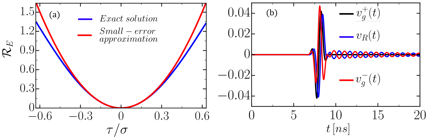
We next evaluate the synchronization sensitivity of the proposed matching scheme for the Gaussian-enveloped sinusoidal incident pulse [Eq. (S9)] by comparing the exact response with the quadratic small-error approximation. As shown in Fig. S4(a), the first-order model accurately reproduces the exact normalized reflected energy for sufficiently small values of , while the discrepancy increases as the timing error becomes larger. Note that the normalized reflected energy exceeds unity for sufficiently large timing errors. This behavior is possible because the system is time modulated, allowing the modulation and bias mechanisms to exchange energy with the circuit and transfer part of that energy to the outgoing wave. To complement the energy-based analysis, Fig. S4(b) shows the temporal profiles of the incident voltage , the reflected voltage , and the voltage across the load resistor for a representative synchronization error. The timing mismatch produces a nonzero reflected waveform and a corresponding deviation of the resistor voltage from the incident pulse. The comparison provides a direct view of how the reflected waveform modifies the voltage delivered to the load resistor. Both the reflected voltage and the resistor voltage exhibit post-pulse ringing associated with the residual transient dynamics of the circuit.
References
- S (1) H. W. Bode, Network Analysis and Feedback Amplifier Design (Van Nostrand, New York, 1945).
- S (2) R. M. Fano, Theoretical limitations on the broadband matching of arbitrary impedances, technical Report No. 41, Research Laboratory of Electronics, MIT, 1948.
- S (3) A. Lapidoth, A Foundation in Digital Communication (Cambridge University Press, Cambridge, UK, 2009).
- S (4) M. A. Pinsky, Introduction to Fourier Analysis and Wavelets (Brooks/Cole, Pacific Grove, CA, 2002).