[1]
[2]
1]organization=Accelerator Technology & Applied Physics Division, E.O. Lawrence Berkeley National Laboratory, city=Berkeley, postcode=CA 94720, country=USA
2]organization=Nuclear Science Division, E.O. Lawrence Berkeley National Laboratory, city=Berkeley, postcode=CA 94720, country=USA
3]organization=Institute for Nuclear Physics, Technical University of Darmstadt, city=Darmstadt, postcode=64289, country=Germany
4]organization=North Carolina State University, city=Raleigh, postcode=NC 27695, country=USA
5]organization=Gamma Reality Inc., city=Richmond, postcode=CA 94804, country=USA
[cor1]Corresponding authors
Characterization of GaN:Si and ZnO:Ga for position-resolved fast timing applications
Abstract
We present the characterization of two fast, crystalline inorganic scintillators, silicon-doped gallium nitride (GaN:Si) and gallium-doped zinc oxide (ZnO:Ga), and compare their performance with cerium-doped yttrium aluminium perovskite (YAP:Ce) for in-vacuum alpha-detection applications that require high-performance timing, position, and energy resolution, such as 3D elemental mapping, medical imaging, and homeland security applications. In this paper, we propose ZnO:Ga and GaN:Si as high-performance drop-in replacements for the alpha detector in Associated Particle Imaging (API) systems. However, the results reported here also have wide applicability. Prior work has reported on polycrystalline forms of ZnO:Ga, which suffer from self-absorption or non-spectroscopic alpha energy spectra, and, to our knowledge, GaN:Si has not been proposed to be used in API systems. We present room-temperature scintillation time constants obtained via X-ray-induced time-correlated single-photon counting for both proposed materials. They both exhibit exceedingly fast rise times of \qty≤15\pico, and high brightness \qty≥1000ph/\megaα with resolved alpha-peaks. Single-crystal ZnO:Ga and single-crystal GaN:Si yield single-component decays of \qty805\pico and \qty32\pico respectively. Using a plastic scintillator reference setup, coincidence timing resolution (CTR) and detector timing resolution (DTR) measurements demonstrate a improvement in timing resolution compared to traditional YAP:Ce. GaN:Si and ZnO:Ga exhibit \qty35 ±9\pico and \qty49 ±5\pico DTR respectively, compared to \qty144 ±2\pico for conventional, single-crystal YAP:Ce. Finally, we evaluate their position resolution in an experimental setup designed for API and measure better than \qty0.2\milli for YAP:Ce and approximately \qty1\milli for GaN:Si. We obtain a position resolution of \qty0.3\milli for ZnO:Ga from simulations. We also present alpha-induced ionoluminescence emission spectra that reveal direct, red-shifted near-bandgap emission.
keywords:
associated particle imaging \septiming resolution \sepfast scintillators \sepZnO:Ga \sepGaN:Si1 Introduction and Background
High-performance radiation detection systems, in particular those achieving fast timing, are of interest to many application domains, from 3D elemental mapping in soils or for planetary exploration to medical imaging, and the detection and imaging of landmines. In medical imaging, Positron-emission tomography (PET) and Computed Tomography (CT) have aspirational timing-resolution targets of \qty≤10\pico coincidence timing resolution (CTR) full width at half maximum (FWHM) [gundacker2019_SiPM_tof-pet]. Reaching this benchmark requires scintillators that are both bright and fast. In PET and CT, improvements in scintillator materials for X-ray and gamma-ray detection are key, and their properties, in a well-engineered system, determine the fundamental limits of performance. Enhancing the scintillator performance would enable, for example, high-precision tumor detection with lower radiation dose for the patient. For 3D elemental mapping, techniques such as Associated Particle Imaging (API) can be applied. For this technique, fast scintillators with good energy and position resolution for alpha particle detection are needed to provide trajectory information of the associated particles (the neutrons). At the same time, the scintillator needs to have low sensitivity to gamma-rays and X-rays. Strong candidate materials exhibit fast detector timing resolution (DTR) performance and short decay constants to enhance API image resolution and reduce pile-up, which can contribute to rate improvements of 10 [ayllon2021_api_3d_recon]. Such improvements would enable high-sensitivity scans for homeland security applications [ji2015_api_SNM], material composition analyses [ayllon2021_api_3d_recon], cross-section measurements, planetary exploration missions [inspect3r], and field-deployed humanitarian de-mining [PavlovskySORMAWest2025]. Although cerium-doped yttrium aluminium perovskite (YAP:Ce) is widely used in current API systems, its intrinsic scintillation properties impose fundamental limits on timing precision, rate capability, and photon statistics, which collectively constrain achievable timing and position resolution. In contrast, silicon-doped gallium nitride (GaN:Si) and gallium-doped zinc oxide (ZnO:Ga) are inorganic semiconductor scintillators with near-band-gap emission and sub-nanosecond decay times, making them intrinsically better aligned with the demands of high-rate, high-resolution API. In this work, we focus on alpha-particle detection using GaN:Si and ZnO:Ga, and compare their performance with YAP:Ce. We measure (i) rise and decay times, (ii) light yield and emission spectra under alpha particle irradiation, (iii) coincidence timing resolution, and (iv) position resolution capabilities of our samples.
1.1 Rise and Decay Times
In previous work, primary decay times were reported to be less than \qty1\nano for GaN:Si (e.g., [schenk2009cathodoluminescence_gan_si]) and ZnO:Ga (e.g., [lehmann1966edge]). While unintentionally doped GaN was studied for its relatively slow yellow luminescence scintillation component, e.g., in yanagida2021photoluminescence_Gan, pittet2009_doping_effect_Si_in_gan have shown that for silicon concentrations on the order of \qty1e19\per\cubic\centi the ultra-fast direct band-gap emission becomes dominant. For GaN:Si at \qty1e19\per\cubic\centi, the decay constant of the fast \qty365\nano scintillation emission was reported to be \qty500\pico by schenk2008gan_si_doping. For ZnO:Ga, cates2013zno_ga measured the decay time of their polycrystalline ZnO:Ga sample to be \qty235\pico and a rise time of \qty20\pico for alpha particle induced time-correlated single-photon counting (TCSPC). As ZnO:Ga has been known for some time for its potential in fast timing applications, growth techniques, and different dopants have been investigated, e.g., by Neal et al. in [neal2008zno_dopant_evaluation] and by bourret2009development.
1.2 Light Yield
yanagida2021photoluminescence_Gan report a light yield of \qty5300 for a \qty5.5 alpha particle for the fast direct bandgap emission of GaN:Si at \qty400\nano. For ZnO:Ga, cates2013zno_ga measured less than \qty750/\megaα from a powder sample, where \qty/\megaα describes the light yield per alpha particle energy. YAP:Ce is a scintillator with a well-known light yield. Crytur, the manufacturer, reports a light yield of \qty5630±630/\megaα, where the error arises from the uncertainty in the alpha-to-gamma ratio, ranging from .
1.3 Statistical Timing Performance Limits
cates2013zno_ga demonstrated sub-\qty100\pico timing at modest detected-photon counts for a ZnO:Ga powder sample and benchmarked results against a straight-response model and the statistical Cramèr-Rao lower bound (CRLB).
A useful way to organize timing analysis for scintillators is to separate (i) the scintillation emission kinetics from (ii) the photodetector time response and the time pickoff. Following seifert2012crlb, we use a straight-response model in which the stochastic emission process is convolved with the Gaussian sensor transit-time spread (TTS), and is then connected to a leading-edge pickoff on the earliest part of the rising waveform. Full derivations and additional background are given in [degroot2012probability, pp. 514–520] as well as in later lower-bound analyses [cates2013zno_ga].
The emission probability density function (p.d.f.), conditioned on photon detection, is denoted . For many materials, the early light is well described by a linear combination of bi-exponential cascades. Writing for the weight of the -th cascade with rise and decay constants and , a convenient normalized, causal form is
| (1) | ||||
Convolving with a normal p.d.f. that describes the photodetector’s carrier TTS produces the p.d.f. for the primary trigger times (conditioned on detection), shifted by the interaction time ,
| (2) |
which we use as the likelihood for estimating (the interaction time). In the straight-response picture, the expected analog waveform at the sensor input is obtained by filtering with the (normalized) single-photon response , and its local slope at a chosen threshold predicts the leading-edge timing jitter. See cates2013zno_ga for details of Eqs. (1)–(5).
If photons are detected and their trigger times are treated as independent and identically distributed samples from , the Fisher information about is
| (3) |
The Cramèr-Rao lower bound (CRLB) on any unbiased time estimator is
| (4) |
In timing applications, one usually reports a FWHM, so the corresponding resolution is
| (5) |
To expose the dominant scaling with scintillation kinetics, consider the single–component limit of Eq. (1) with negligible rise time () and negligible sensor , such that . In this regime, , and inserting into Eq. (3) yields
| (6) |
Using Eq. (4), the variance therefore satisfies
| (7) |
and consequently
| (8) |
Thus, once the rise time and detector jitter no longer dominate, the achievable timing resolution scales linearly with the decay constant and inversely with the square root of the detected-photon statistics. cates2013zno_ga show that for well–conditioned signals (low noise, high gain) and with an optimized leading–edge pickoff on the earliest rise, measured resolutions can closely approach this statistical limit.
1.4 Position Resolution
ayllon2021_api_3d_recon characterized the position resolution capabilities of a YAP:Ce scintillator in an integrated API system and reported an achievable alpha particle resolution using a Hamamatsu H13700-03 SEL photomultiplier tube (PMT) of less than \qty0.2\milli. For ZnO:Ga, cates_zno_pos_res report a position resolution of less than \qty1\milli for \qty80 of the detector area.
2 Samples studied in this Work


Three different scintillator samples were studied in this work and are shown in Figure 1. The GaN:Si sample consisted of a \qty50\milli-diameter, \qty430\micro-thick sapphire wafer bearing epitaxially grown layers: \qty1.5\micro of unintentionally doped GaN and a \qty10\micro silicon-doped GaN film with a silicon concentration of \qty7e18\per\cubic\centi. An additional \qty250\nano Al coating was deposited on the top surface to enhance light-collection efficiency. The structure was grown by metal-organic vapor-phase epitaxy (MOVPE) and provided by the group of Michał Boćkowski (Institute of High-Pressure Physics, Polish Academy of Sciences, Warsaw).
The ZnO:Ga sample was a bulk single-crystal with lateral dimensions of \qtyproduct10 x 10\milli and a thickness of \qty0.5\milli. One face was polished. The crystal was doped with gallium at a concentration of , purchased from MTI Corporation, and supplied by Gamma Reality Inc.
Finally, the YAP:Ce sample consisted of a \qtyproduct50 x 50 x 1 YAP:Ce single-crystal grown by Crytur. A \qty400\nano Al coating was applied to the surface to improve light collection.
2.1 Scintillation Properties
The luminescence of the wide-bandgap semiconductor GaN:Si is governed by a competition between near-band-edge recombination and defect-related emission bands. At room temperature, the direct bandgap of GaN is near \qty3.4, corresponding to ultraviolet emission around \qty365\nano (see, for example, pittet2009_doping_effect_Si_in_gan). For heavily Si-doped material, the radiative efficiency increases due to enhanced band-to-band recombination rates [schenk2008gan_si_doping]. In addition to band-edge emission, a broad yellow luminescence band centered around \qty540\nano is typically observed. This band is commonly attributed to deep defect complexes such as Ga vacancies combined with oxygen or carbon impurities, which act as deep acceptors.
ZnO:Ga is another wide-bandgap semiconductor with a band edge around \qty3.37. The dominant radiative mechanism involves recombination of electrons from Ga3+ donor levels with ionized holes trapped at shallow acceptors, most effectively hydrogen ions bound to zinc vacancies. bourret2009development have shown that processing ZnO with Ga2O3 followed by hydrogen annealing minimizes defects, resulting in high luminosity and stable sub-nanosecond decay. This donor–acceptor channel produces bright emission centered near \qty389\nano, slightly below the band edge by about \qty0.18, and explains the ultra-fast, spectrally pure scintillation observed in an optimally prepared sample. In this study, the emission peak of the ZnO:Ga sample is at \qty401\nano, which suggests strong self-absorption in our relatively thick sample for the \qty389\nano emission peak reported by bourret2009development. Therefore, unlike GaN:Si, high-quality ZnO:Ga shows little contribution from deep-level luminescence, and its performance is set by the balance between Ga donor electrons and shallow acceptors created during processing.
2.2 Self-Absorption in GaN:Si and ZnO:Ga
Both GaN:Si and ZnO:Ga exhibit strong self-absorption of their emitted light because the emission lies close to the band gap — only about \qty0.07 below the band edge in GaN:Si and \qty0.18 below the band edge in ZnO:Ga. The Urbach tail describes absorption near the band edge as a function of the energy difference between the emission and the gap, [cremades2000GaN_Si_absorption_doping_carrier_concentration]:
| (9) |
where is the absorption coefficient at the emission energy, is the band-edge absorption coefficient, and is the Urbach energy, a measure of the tail width. In heavily doped GaN:Si, for example, a doping level of about \qty8e18\centi^-3 may yield [cremades2000GaN_Si_absorption_doping_carrier_concentration] and for ZnO:Ga [yilmaz2015ZnO_Ga_Urbach_tail]. Because the emission energy lies only slightly below the band gap in both materials, the absorption coefficient remains high in the emission region: evaluating at gives for ZnO:Ga and for GaN:Si. At the band-edge energy, the absorption coefficients are for GaN:Si and for ZnO:Ga [schenk2009cathodoluminescence_gan_si], which yield for GaN:Si and for ZnO:Ga. In contrast, in a host such as YAP:Ce with a much larger band gap of \qty8.1 [yu2015energy], the dopant emission at \qty370\nano lies far below the absorption edge and is transmitted with negligible reabsorption.
3 Experimental Methods
Rise and decay times are obtained via X-ray-induced TCSPC, which probes the intrinsic scintillation kinetics of each material and provides results that are broadly applicable regardless of the excitation particle type. Light yield, CTR, and position resolution are measured under direct alpha particle irradiation, making the results specific to alpha detection applications such as API. The timing framework and CRLB analysis, however, are general and applicable to broader contexts, including PET and CT.
3.1 Time-Correlated Single-Photon Counting Setup
To quantitatively characterize the scintillation kinetics of the different samples and to calculate the CRLB according to Eq. (5), time-correlated single-photon counting measurements were performed. The experimental setup, shown in Figure 2, employed an ultra-short pulsed \qty200\femto Ti:Sapphire laser with frequency-doubled output (via second harmonic generation), pumped by a Nd:YAG laser operating at its second harmonic. The light from the Ti:Sapphire laser served both as the start reference and as the driver for a photo-excited X-ray tube (Hamamatsu N5084) operating at \qty40\kilo. The emitted X-rays excited scintillation light in the samples, which was collected by a Hamamatsu R3809U-50 microchannel plate PMT (MCP-PMT) with an intrinsic TTS of \qty25\pico FWHM. Photon arrival times were digitized with a PicoHarp 330, which uses constant fraction discrimination (CFD) for accurate time-stamping of the start and stop signals and records their time differences. An older version of this setup is described by derenzo1992design_tcspc. The instrument response function (IRF) of the system, assumed to be Gaussian, has been improved since the original publication of the design from \qty109\pico to about \qty68\pico FWHM. The IRF of the system was measured using a PbF2 sample. While the IRF is not perfectly Gaussian, a Gaussian fit was used to estimate its FWHM. Since the original publication of the design, the IRF has been improved from \qty109\pico to about \qty68\pico FWHM. The timing resolution is predominantly limited by the response of the pulsed X-ray tube, whereas contributions from the PMT transit time spread ( \qty25\pico) and the excitation pulse duration ( \qty200\femto) are comparatively small.

3.2 Light Yield Measurement Setup
To measure the absolute light yield of the GaN:Si, ZnO:Ga, and YAP:Ce samples in the setup shown in Figure 3, the single-photon response of the Hamamatsu R9800-100 PMT with the DRS4 evaluation board data acquisition system was first quantified.

3.2.1 Single-Photon Response Setup

The experimental setup to measure the single-photon response is shown in Figure 4. An LED was pulsed at \qty500 with a pulse duration of \qty150\nano. The same pulse was used to trigger the data acquisition system. Varying the applied LED voltage produced a shift in detected photons.
3.2.2 Photon Transport Efficiency Simulation
To derive the number of photons created by a charged particle in a scintillator from the number of detected photoelectrons (p.e.), one must account for the photon-transport efficiency from the scintillator into the PMT. The geometry for this is shown for the GaN:Si sample in Figure 3. A similar geometry was used for the ZnO:Ga and YAP:Ce samples. Using a Monte Carlo photon transport simulation (see Figure 5), the photon-transport efficiency is defined as the fraction of photons arriving at the PMT. For GaN:Si, ZnO:Ga and YAP:Ce, the photon transport efficiency was simulated to be \qty18.9±0.2, \qty23±0.2 and \qty34.5±0.3, respectively. The simulation assumes that all photons are created at a single point in space and time, which is a valid approximation for the bulk materials used in this study, where particle ranges are less than \qty15\micro and stopping times are less than \qty2\pico. The simulation models absorption and transmission using the Beer–Lambert law and the Fresnel equations. The main reason for photon losses is the index of refraction mismatch. The values for indices of refraction, absorption coefficients, and the thickness of the relevant layers used in the simulation are summarized in Table 1. Note that only for the GaN:Si sample there is a sapphire layer between the substrate and the optical grease to couple to the borosilicate glass PMT window.
| Material | (\qty\nano) | (\qty\centi^-1) | Layer (\qty) | |
| YAP:Ce | 1.931 | 370 | ||
| GaN:Si | 2.505 | 372 | 2470 | |
| ZnO:Ga | 1.706 | 401 | 2160 | |
| Sapphire | 1.793 | n.a. | ||
| Opt. grease | 1.466 | n.a. | ||
| PMT glass | 1.535 | n.a |

3.3 Coincidence Timing Resolution Setup
6(a) shows the setup used to characterize the DTR of the GaN:Si sample. This setup is adapted from the setup developed by cates2013zno_ga. The same configuration was used for YAP:Ce and ZnO:Ga. Three Hamamatsu R9800-100 super bialkali-PMTs were used to detect photons from the reference plastic scintillator and each sample scintillator. The TTS of \qty115\pico (\qty270\pico FWHM) was taken from the Hamamatsu datasheet. A DRS4 evaluation board served as the data-acquisition system, offering \qty700\mega of analog bandwidth and a sampling rate of \qty5e9\per across four channels in coincidence.


The alpha particles from a \qty40\nanoCi \qty5.47\mega 241Am source, covered with a thin gold layer, first pass through a thin EJ-214 plastic scintillator (Eljen Technology) before they are stopped in the sample. 6(b) shows the EJ-214 film sandwiched between two polymethyl methacrylate (PMMA) light guides. The space between the PMMA slabs is filled with optical grease, and the assembly is wrapped in Teflon to increase reflectivity. The EJ-214-PMMA light guide structure is optically coupled to two Hamamatsu R9800-100 PMTs, one on each side, so that a single alpha event is detected in both PMTs. According to SRIM/TRIM simulations [SRIM], alpha particles deposit about \qty2.9\mega in the EJ-214 film and lose a total of about \qty700\kilo while traversing the \qty4\milli of air gaps between the source, the EJ-214, and the scintillator, so that \qty1.9\mega are deposited in each scintillator sample.
3.4 Position Resolution Measurement Setup
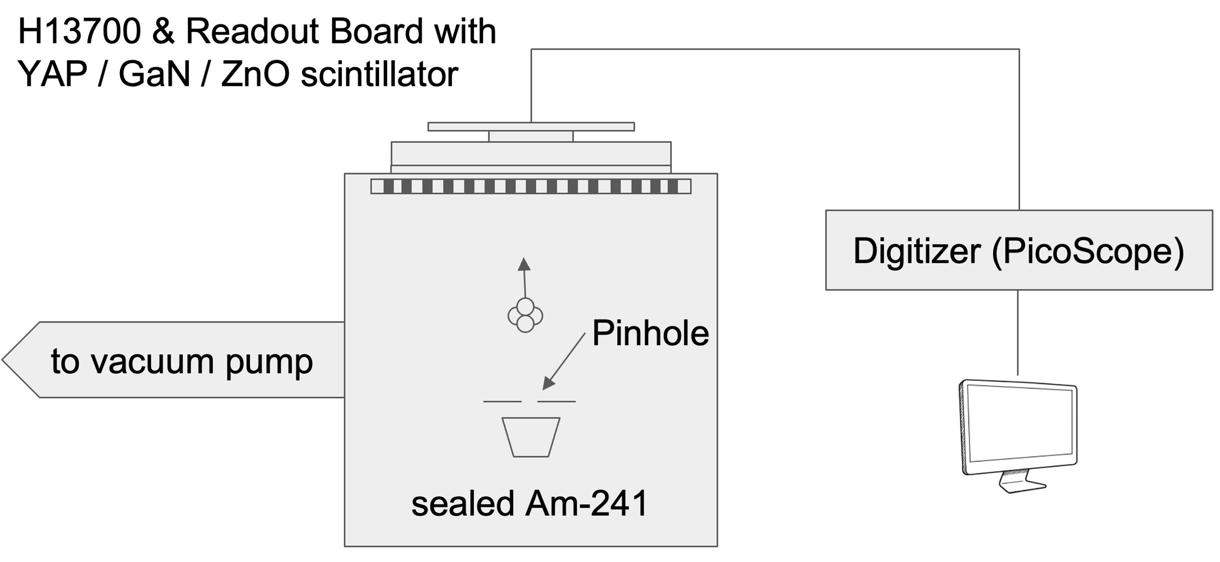


An 241Am source was placed inside a vacuum chamber at a distance of about \qty8\centi from the GaN:Si, ZnO:Ga, and YAP:Ce crystals. Figure 7 shows the experimental setup.
The crystals were covered with the masks shown in Figure 8 to reconstruct the position resolution. Photons created in the crystals passed through a thin vacuum gap and a sapphire window, which served as the vacuum interface, into a Hamamatsu H13700-03 PMT with \qtyproduct16 x 16pixels (\qtyproduct3 x 3mm pixel pitch) and a total active width of \qty48\milli. This geometry is required not only to ensure that alpha particles have a line of sight to all parts of the PMT but also to emulate the scintillator’s implementation in an integrated API system, as studied by ayllon2021_api_3d_recon.
The pixelated PMT was read out with a custom board described in [ayllon2021_api_3d_recon]. It uses a resistive network to encode the photon-impact position into four output channels. By integrating the signals on those four channels and computing the center of mass, a 2D interaction position is obtained.
4 Results and Discussion
4.1 Rise and Decay Time Results


Figs. 9(a), 9(b), and 9(c) show the measured TCSPC histograms for GaN:Si, ZnO:Ga, and YAP:Ce. The insets show the same plots with a linear y-scale, and the fit residuals are shown below each TCSPC histogram. The waveform-shaped histograms reflect the convolution of the true scintillation decay with the IRF. Equation (1) was used as the fitting model, and a least-squares procedure was applied to extract characteristic rise and decay components. The fit results are summarized in Table 2. For YAP:Ce, the distribution shows a comparatively slow decay typical of Ce-activated oxides. By integrating a long (\qty165\nano) and a short (\qty10\nano) interval of the pulse, we obtain that about \qty30 of the total light yield is emitted in the first \qty10\nano. In contrast, ZnO:Ga exhibits a sharp, sub-nanosecond peak consistent with its ultra-fast donor-acceptor recombination mechanism. We measured that about \qty98 of the total light yield is emitted in the first \qty10\nano. GaN:Si shows intermediate behavior, with an ultra-fast near-band-edge component and an additional slower tail from defect-related recombination. Note that the slow component of \qty16\nano contributes only about \qty0.5 to the pulse shape. The small peak in the primary decay in 9(a) is likely related to instrumental artifacts. We measured that about \qty80 of the total light yield is emitted in the first \qty10\nano.
The quality of the fits and the agreement of the residuals confirm that the Gaussian IRF assumption is adequate to deconvolve the observed distributions. This analysis highlights the very different timing profiles of the three scintillators: ZnO:Ga as an ultra-fast benchmark, YAP:Ce as a high-yield but slower reference, and GaN:Si as a promising ultra-fast material that surpasses the well-established ZnO:Ga in terms of timing and decay time but falls below ZnO:Ga in light yield.
| Material | Rise times | Decay times |
| GaN:Si | \qty9.8 ±2.7\pico | \qty32.4±1.0\pico (95.8%) \qty269±7\pico (3.7%) \qty16.0±0.5\nano (0.5%) |
| ZnO:Ga | \qty≤5\pico (71%) \qty403±9\pico (29%) | \qty805±1\pico (99.98%) \qty7.3±0.3\nano (0.02%) |
| YAP:Ce | \qty175±1\pico | \qty24.3±0.1\nano (95%) \qty106±0.4\nano (5%) |
4.2 Light Yield Results


4.2.1 Single-Photon Response Results
To calculate the absolute light yield of the samples used in this work, both the single-photon response and the quantum efficiency (QE) of the PMT must be known. We used Poisson statistics to extract the single-photon response from the pulsed LED setup discussed in Section 3.2.1, as shown in Figure 10. All recorded waveforms, triggered on the signal from the pulse generator, were integrated over a fixed time window, independent of whether a photon signal was present. As a result, the distribution includes events with zero detected photoelectrons, forming a pedestal peak centered around zero integrated signal, which corresponds to the electronic noise floor. The full distribution was modeled as a sum of Gaussian contributions corresponding to 0, 1, 2, and higher photoelectron events. The separation between adjacent peaks defines the single-photoelectron response, while the width of each Gaussian reflects the combined effects of electronic noise and gain fluctuations. While the width of the distribution for 0 p.e. is goverend by noise only, the width of the events with 1 or more p.e. also includes the photon response function of the PMT. We verified this method to obtain the single photon light yield using an independent approach: by identifying single-photon pulses in individual traces across different LED intensities, we constructed a median pulse shape where the integral agrees well with the single-photoelectron response extracted from the multi-Gaussian fit.
The same measurements were repeated for the other two R9800-100 PMTs that are used later in the timing experiments. While the single-photon light yield uncertainty of about \qty32 () drives the overall uncertainty of the light-yield calculation, the variation of the mean single-photon light yield among the three PMTs was measured to be less than \qty4.
4.2.2 Absolute Light Yield Results
The R9800-100 PMT has a QE of \qty42 at \qty400\nano. At \qty1300, the typical gain is about . The R9800-100 has been studied in detail by seng2013_R9800_study. Additionally, Monte Carlo photon transport simulations were performed to account for photon-transport efficiency. 11(a) shows a direct comparison of the measured photoelectrons for each sample. Note that the ZnO:Ga measurement was performed without a reflective mirror coating, whereas GaN:Si and YAP:Ce employed reflective coatings. The integration window for GaN:Si and ZnO:Ga was \qty25\nano while \qty165\nano of the waveform were integrated for YAP:Ce due to the slower decay. The energy resolution of \qty8.8 FWHM measured for ZnO:Ga is noteworthy, given that the statistical limit is \qty6.9 for ZnO:Ga corresponding to the statistical limit . Eq. (10) provides the formulas used to obtain the absolute light yields for alpha particles shown in 11(b):
| (10) | ||||
Here, is the number of photoelectrons detected by the PMT, qe is the quantum efficiency of the PMT, is the photon-transport efficiency from the scintillator to the PMT, is the energy of the incident alpha particle in MeV, and is the light yield in photons per MeV.
Although the single-photon response dominates the overall uncertainty, the measured value for YAP:Ce agrees well with the manufacturer’s reference. The monocrystalline ZnO:Ga sample, as expected, significantly outperforms powder samples in light yield. The relative light yield is approximately 17% for GaN:Si and 43% for ZnO:Ga compared to YAP:Ce. One contributor to the lower detected-photon fraction for GaN:Si is its high refractive index, which increases reflections at interfaces and narrows the total internal reflection acceptance cone. Table 3 summarizes the detected number of photons, material properties, and calculated light yield.
| Material | Detected p.e. | Calc. light yield (ph/MeVα) | |
| GaN:Si | 1060 350 | ||
| ZnO:Ga | 2600 860 | ||
| YAP:Ce | 6090 2010 |
4.2.3 Ionoluminescence Spectra
Ionoluminescence is the emission of light from a material as a result of excitation by energetic ion irradiation, analogous to radioluminescence induced by X-rays or gamma rays. Transmission ionoluminescence spectra were collected by irradiating the GaN:Si and ZnO:Ga samples with -particles from a 241Am source. The emitted light was analyzed using a SpectraPro-2150i spectrometer (Acton Research), coupled to a Pixis:1008 CCD camera (Princeton Instruments). In the transmission geometry, the ionoluminescence was detected from the side opposite to the irradiated face, ensuring that only light transmitted through the sample was measured. All spectra were corrected for the instrument response. The resulting ionoluminescence spectra for both materials are shown in Figure 12.

While ZnO:Ga exhibits a single strong emission around \qty401\nano, GaN:Si shows the direct bandgap emission at \qty372\nano and, in addition, the greenish yellow luminescence peaking around \qty567\nano, as also reported by yanagida2021photoluminescence_Gan and TOMINAGA2026117697. The contribution from the fast-bandgap emission is significantly higher than in the unintentionally doped GaN sample reported in yanagida2021photoluminescence_Gan. The correlation between the fast decay and the \qty372\nano emission was verified by TCSPC measurements with and without wavelength filters: with a \qtyrange360380\nano filter, the GaN:Si decay shows only the ultra-fast component, whereas the slow \qty16\nano component shown in 9(a) is absent.
4.3 Coincidence Timing Resolution Results
4.3.1 Experimental Results


| Material (PMT) | Photons [p.e.] | CFD parameters |
| GaN:Si (1) | \qtyrange210260 | d=\qty1\nano, f=\qty0.53 |
| EJ (2,3) | \qtyrange220260 | d=\qty2.8\nano, f=\qty0.2 |
| ZnO:Ga (1) | \qtyrange700840 | d=\qty0.8\nano, f=\qty0.32 |
| EJ (2,3) | \qtyrange280330 | d=\qty2.8\nano, f=\qty0.2 |
| YAP:Ce (1) | \qtyrange19002650 | d=\qty0.8\nano, f=\qty0.35 |
| EJ (2,3) | \qtyrange230280 | d=\qty2.8\nano, f=\qty0.2 |

For all three samples, a total of \qty200000 traces were collected in the triple coincidence setup described in Section 3.3: one per channel for the two reference EJ-214-coupled PMTs and the sample-coupled PMT. Because the probability of accidental (random) coincidences is negligible with triple-coincidence triggering, no additional event selection was required. Figures 13(a), 13(b), and 13(c) show the timing uncertainty to detect individual alpha particle events in CTR histograms for each sample (left) and the reference EJ-214 scintillators (right).To determine the trigger time in each channel, a custom CFD was implemented based on the recorded trace data. The CFD was calculated using Eq. (11):
| (11) |
where is one individual digitized and interpolated waveform, represents the delay and is the fraction. A CFD optimization was performed to find the optimal parameters for each sample and the EJ-214 thin film. The optimized values are summarized in Table 4. The table also captures the photon windows of the traces selected to measure the CTR. As the CRLB and the experimentally achievable timing performance vary with the number of photons in each waveform, we selected narrow photoelectron windows (used as an energy proxy) for the signal in our collected traces. All three samples showed a Gaussian-like energy spectrum as seen in 11(a), from which we selected an energy/photon window around the peak. However, in this setup, we now only have about \qty1.9\mega alpha particles instead of \qty5.47\mega alpha particles presented in Section 4.2, and therefore, the total number of detected photons is lower.
Time of flight of the alpha particles contributes only a constant offset between the mean photon-arrival times at the reference PMTs and the sample PMT. However, the event-to-event spread is governed by the convolution of the sample and EJ-214 CTR contributions together with TTS and electronic jitter. To calculate the contribution of the sample scintillators, we use
| (12) | ||||
where FWHM is the measured FWHM of the CTR distribution in the right panel of each figure, and FWHM is the measured FWHM of the CTR distribution on the left. The factor of assumes that both EJ-coupled PMTs contribute equally to the EJ+EJ timing distribution, which is justified by the measured variation of less than \qty4 in single-photon response among the three PMTs. To compare FWHM with the theoretically possible CRLB, the photon-selection windows were chosen for each material to optimize the CTR and its uncertainty. Figure 14 presents the resulting FWHM DTR and the CRLB for each material. A central result is the measured DTR of \qty35 ±9\pico for GaN:Si and \qty49 ±5\pico for ZnO:Ga. Note that for ZnO:Ga this is similar to the result reported by cates2013zno_ga for a powder ZnO:Ga sample, although the PMTs used in that work had a significantly faster TTS. This suggests that the higher photon yield of the single-crystal compensates for the slower TTS of the Hamamatsu R9800-100 PMTs.
4.3.2 Statistical Timing Resolution Limits


To understand the prospects for even better timing performance with GaN:Si and ZnO:Ga, Figure 15 shows the theoretically achievable CRLB for the DTR as a function of detected photoelectrons and the TTS FWHM of the PMT. For this, the rise and decay times for both samples from Section 4.1 were inserted into Eq. (1) to obtain the emission p.d.f., which was then used in Eq. (2) to calculate the CRLB via Eqs. (3), (4), and (5). With a photodetector with a TTS FWHM below \qty100\pico and a similar QE and therefore a comparable number of detected photons, timing resolutions on the order of \qtyrange1020\pico are theoretically achievable with GaN:Si and ZnO:Ga. Especially for GaN:Si, one can obtain from 15(a) the potential for a CRLB down to \qty10\pico, making it a very suitable candidate for ultra-fast timing applications. Note that the number of detected photons for the ZnO:Ga sample could be significantly increased by adding a reflective layer as was done for the two other samples.
4.4 Position Resolution Results
4.4.1 Experimental Results


Figure 16 shows a qualitative comparison of the position-resolution capabilities for ZnO:Ga, GaN:Si, and YAP:Ce. Because total internal reflection at the sample–vacuum interface is a major loss mechanism, the light yield in this geometry is significantly lower than in Section 3.2. We measured approximately 25% of the photoelectron yield obtained in the light yield setup Section 4.2: about \qty1000 p.e. for YAP and \qty90 p.e. for GaN with the H13700-03. A four-channel PicoScope D6404 with \qty500\mega bandwidth and a sampling rate of \qty1.25GS/s was used to acquire the data. For ZnO:Ga (upper right), only a small fraction of the H13700-03 PMT was covered with the scintillator, and therefore only seven grid points are visible. For YAP:Ce (lower left), surrounding grid points are distorted due to edge effects in the PMT (see e.g. ayllon2021_api_3d_recon for more details on edge effects). GaN:Si (lower right) shows a coarser image with reduced resolution. The sample’s round shape is clearly visible.
Additionally, a finer mask was placed inside the vacuum chamber on top of the GaN:Si and YAP:Ce samples to replace the coarse mask for a more quantitative assessment of the position resolution. The ZnO:Ga sample could not be measured with this mask because its small lateral size (\qtyproduct10 x 10\milli) did not extend to the fine mask holes, which are located off-center in the field of view. The measurements with that mask, which has hole-to-hole distances from \qty0.2\milli to \qty1.4\milli, are shown in Figure 17. In agreement with ayllon2021_api_3d_recon, the position resolution for YAP:Ce is at least \qty0.2\milli, whereas resolving two holes with GaN:Si is noticeably more difficult. We note that GaN:Si achieves a position resolution of approximately \qty1\milli, which is adequate for many API imaging scenarios.
4.4.2 Position Resolution Simulations


To quantify the position-resolution capabilities of the ZnO:Ga sample, we performed Monte Carlo simulations using the same Python code as in Section 3.2. For each sample, the number of photons was drawn from the measured distribution. In Figure 18, the upper panel shows the distribution of photons arriving at the PMT after the photon-transport simulation. In contrast, the lower panel shows the integrated per-pixel signal and the reconstruction derived from it. The H13700-03 has a pixel size of \qtyproduct3 x 3\milli. The simulation was repeated 500 times for each sample. Figure 19 shows the distribution of reconstructed positions, which ideally cluster at the origin. The spread of this distribution serves as a measure of the achievable position resolution.
For YAP:Ce and GaN:Si, the results agree with the measurements in Section 3.4. The slightly worse measured position resolution for GaN:Si can be explained by the data acquisition system, which reduced energy resolution and therefore spatial resolution due to the comparatively low sampling rate of \qty1.25GS/s, where the pulse shape of a GaN:Si signal is sampled by only a few points. For ZnO:Ga, two simulations were run: the first represents the sample used in this work and shows that, like the measured light yield, the achievable position resolution is between YAP:Ce and GaN:Si, closer to the performance of GaN:Si. However, when a thinner sample (\qty100\micro, reducing self-absorption) was used and coated with a mirror layer on one side, the light yield increased substantially, improving the position resolution by more than 30% to about \qty0.2\milli.
5 Conclusions
We characterized single-crystal ZnO:Ga and near-single-crystal GaN:Si for in-vacuum alpha-particle detection, demonstrating fast timing, energy-resolved alpha peaks, and high position resolution relevant to API applications. To our knowledge, the use of GaN:Si in API systems is novel. We show that these crystals achieve a improvement in timing resolution over YAP:Ce, a commonly used high-performance scintillator in such systems. Using TCSPC, we extracted rise and decay components. We quantified absolute and relative light yields, and measured the CTR as well as the resulting DTR of our samples in an alpha particle triple-coincidence setup. The main experimental results are summarized in Table 5: (i) primary decay components of \qty32.4±1\pico for GaN:Si, \qty805±1\pico for ZnO:Ga and \qty24.3±0.1\nano for YAP:Ce, (ii) absolute light yield of \qty1060 ±350ph/\megaα (GaN:Si), \qty2600 ±860ph/\megaα (ZnO:Ga), \qty6090 ±2010ph/\megaα (YAP:Ce), (iii) DTR of \qty35 ±9\pico for GaN:Si and \qty49 ±5\pico for ZnO:Ga compared to \qty144±2\pico for YAP:Ce, and (iv) position resolution of at least \qty0.2\milli for YAP:Ce, about \qty1\milli for GaN:Si, and expected \qty0.3\milli for ZnO:Ga, and down to \qty0.18\milli with a reflective layer in a thinner geometry. Our CRLB analysis indicates that with PMTs, MCP-PMTs or silicon-photomultiplier achieving TTS FWHM and comparable QE, GaN:Si and ZnO:Ga could, in principle, support DTR near or even below \qty10\pico.
| GaN:Si | ZnO:Ga | YAP:Ce | |
| Primary [] | |||
| LY [ph/α] | |||
| peak [] | 372 | 401 | 365 (Crytur) |
| CTR [] | |||
| Pos. res. [] | (est.) |
From a systems perspective, faster decay and reduced pile-up open a path to higher operational rates and finer depth resolution in an integrated API system. While accidental coincidences remain a limiting factor at elevated neutron rates, improved CTR can narrow the coincidence window for certain applications where it is limited by the CTR and not neutron time of flight within the region of interest, and can therefore lower the random-coincidence rate.
Practical limitations are self-absorption and total internal reflection at sample-vacuum interfaces, which reduce the effective light yield (especially for ZnO:Ga/GaN:Si near the band edge). At the same time, optical design (thinning, reflective layers, index matching) measurably improves both collection efficiency and position resolution.
Data availability
All data used in this work and all scripts to recreate the plots shown in this work can be found on Zenodo [zenodo].
Acknowledgement
We thank Michal Boćkowski from the Institute of High Pressure Physics of the Polish Academy of Sciences for providing the GaN:Si sample. We also want to thank Takeshi Katayanagi for technical support at LBNL.
This work was supported by the NASA PICASSO program under grant No. 22-PICASSO22-0013. Work at Lawrence Berkeley National Laboratory was conducted under U.S. Department of Energy Contract No. DE-AC02-05CH11231.