First-principles finite-size correction schemes for point defects of Cu3N
Abstract
Point defects play a key role in determining semiconductor properties, such as electrical conductivity and photoluminescence, and often enable functional behavior. Accurate first-principles supercell simulations of point defects require reliable finite-size corrections. In this study, we combine PBE+U structural relaxations with HSE hybrid-functional calculations to determine defect formation energies and thermodynamic transition levels of Cu3N. Finite-size trends are quantified using -point calculations in supercells containing 256, 864, and 2048 atoms. We assess and extend the Makov-Payne and Lany-Zunger correction schemes by introducing additional terms, together with core-level potential alignment and defect-specific scaling models. Using Cu3N as a case study, we show that charged vacancies with strongly localized defect states are accurately described by the Makov-Payne-type scaling (), whereas interstitial defects with shallow or weakly localized electronic character are better captured by a hydrogenic impurity model that accounts for defect-band dispersion. Residual trends for neutral or weakly localized defects are described by higher-order polynomial fits in and . Hybrid-functional energetics corrected using PBE+U-based finite-size trends confirm the intrinsic -type character of Cu3N under the conditions considered and demonstrate that no single finite-size correction can be transferred across all defect types.
I Introduction
Point defects in semiconductors correspond to single lattice site imperfections in an otherwise periodic crystal. These include interstitials (Xi) and vacancies (VX) of an atom , as well as substitutions (YX) of a host atom by atom . Intrinsic defects comprise cases in which the species involved are the same as those that form the host material, while extrinsic defects include species not present in the pristine crystal. Typically, defect concentrations are low, e.g., parts per million, and are driven by Maxwell-Boltzmann thermodynamics. Despite their low concentration, point defects are responsible for key properties of semiconductors, such as electrical conductivity and photoluminescence spectra [1, 2], which, in turn, have important implications and functional properties in modern electronics [3], solar energy conversion [4, 5, 6], and batteries [7].
Theoretical studies of point defects generally rely on first-principles density functional theory (DFT)-based calculations and the supercell approach [8], with varying degrees of sophistication [9]. Within the DFT supercell approach, practical cell sizes correspond to defect concentrations that are far above the dilute limit, leading to artificial interactions between the defect and its periodic images. Consequently, the calculated formation energies of charged defects are affected by (i) spurious long-range Coulomb interactions and (ii) the arbitrary choice of the average electrostatic potential, which shifts the energy scales of supercells with different charges and/or numbers of atoms. To recover the dilute limit, we therefore introduce a defect-dependent finite-size correction to the formation energy.
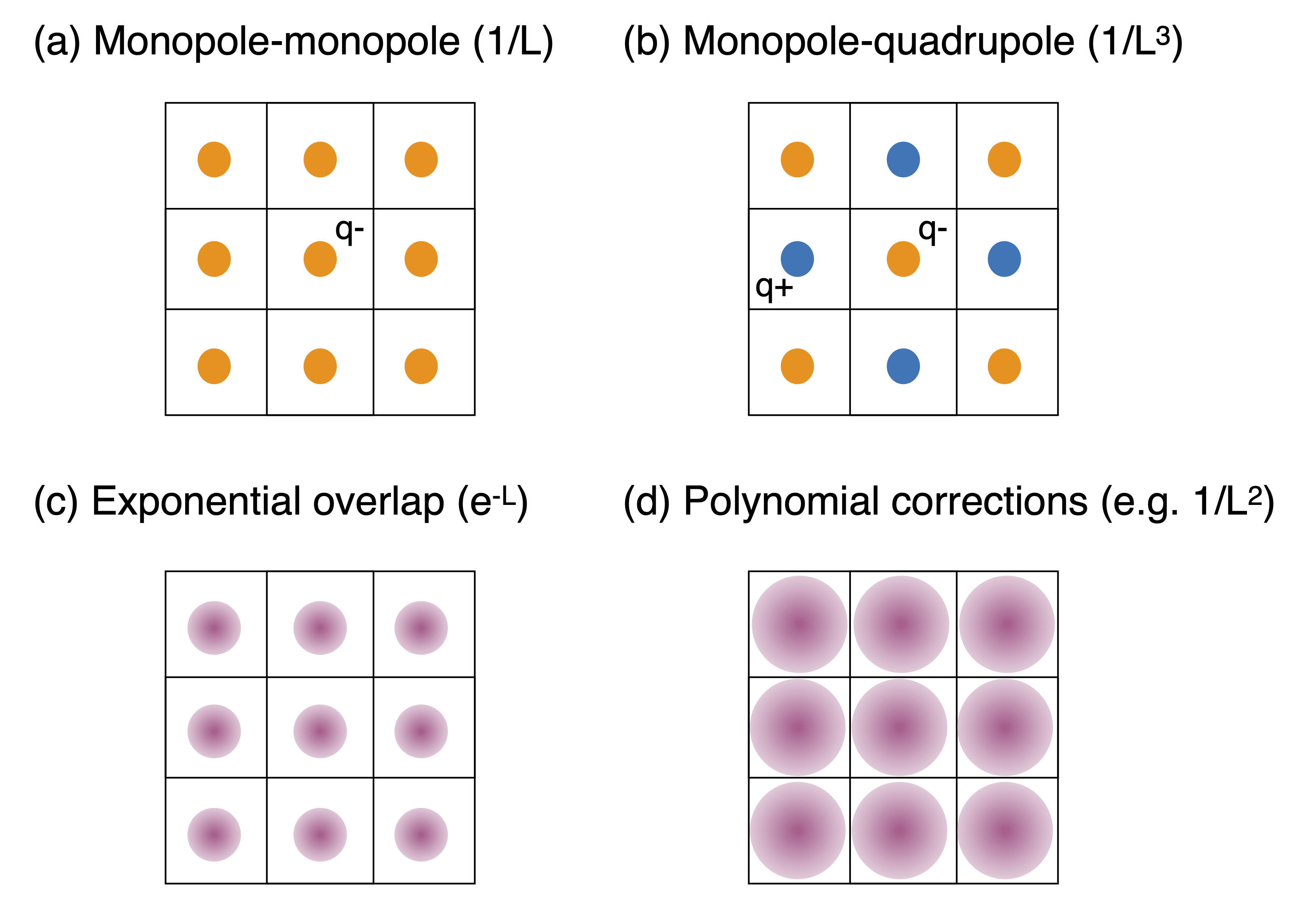
Figure 1 shows dominant spurious electrostatic interactions between a charged defect and its periodic images [10, 11]. The widely used correction method of Makov and Payne [12] assumes a strong excess charge around the defect and incorporates quadrupole effects (see Fig. 1(a) and (b)). The finite-size correction of Makov-Payne is obtained from a multipole expansion, retaining the monopole–monopole () and monopole–quadrupole () terms, as
| (1) |
where is the defect charge, is the lattice Madelung constant of the supercell, is the (static) dielectric constant of the host, is the characteristic linear size of the supercell, and is the quadrupole moment of the defect charge distribution. Several alternative finite-size correction schemes have also been proposed [13, 14, 15, 16]. In addition, the relative zero of the formation energy, originating from the mismatch of charge and stoichiometry among different supercell calculations, is corrected by adding the “potential alignment” term
| (2) |
where is the defect charge, and is the far-field electrostatic potential offset of the defective cell with respect to the pristine reference , commonly evaluated using core-level–averaged potentials [17, 14].
Notably, test calculations with very large supercells show that, for a number of defects, the combination of the Makov-Payne correction and the potential alignment converges towards the dilute limit [15]. These results also show that the monopole-quadrupole correction can be proportional to the monopole-monopole correction, implying a dependence of the defect quadrupole . Therefore, the finite-size correction method of Lany and Zunger proposes
| (3) |
where the potential alignment correction is typically proportional to , and the factor accounts for the proportionality between the monopole-quadrupole and monopole-monopole terms.
Another popular approach is the finite-size (FS) scaling method [15], which involves calculating the defect finite-size correction energy by employing a sequence of supercells with increasing size , and fitting the defect formation energy with the function
| (4) |
Eq. (4) implies a size correction
| (5) |
where and are obtained as fitting parameters. Let us note that if Eqs. (1) or (3) apply, then .
While the methods of Makov-Payne and Lany-Zunger (see Eqs. 1 and 3) have the advantage of offering a fast correction method without the need for a sequence of computationally expensive calculations with larger supercells, the finite-size scaling method (see Eq. (5)) allows for the assessment of size effects for defects that have not been explored previously.
Previous DFT studies using the supercell approach and the correction methods described above have critically examined the performance and applicability of existing a posteriori schemes, including the Makov-Payne, Lany-Zunger, and Freysoldt-Neugebauer-Van de Walle (FNV) methods [14], and have established the conditions under which these approaches can be reliably applied, concluding that the FNV scheme generally provides the best performance for defects with localized electronic states, regardless of the material [18, 19]. This body of work has enabled accurate calculations of defect properties relevant to photovoltaics, photocatalysis, and batteries [20, 16, 21]. However, despite this progress, several classes of point defects still exhibit deviations from these standard models, and their formation-energy corrections are not well described by Eqs. 1–5 [11]. These deviations can arise from additional long-range interactions not captured by the Makov-Payne and Lany-Zunger schemes, such as monopole-dipole interactions (), dipole-dipole interactions in the neutral case (), and residual interactions (). In addition, short-range interactions originating from lattice stress () and defect-wavefunction overlap () may not be sufficiently attenuated in commonly used small to medium supercells and may also require further correction.
In this work, we use first-principles methods to investigate the performance of the Makov-Payne and Lany-Zunger finite-size correction methods when additional terms are included. As a case study, we investigate the low-energy defect properties of copper nitride (Cu3N), a material of interest for solar energy conversion and optoelectronic devices [22, 23, 24, 25]. Cu3N can host a diverse array of defect types and, therefore, provides a useful platform for identifying distinct finite-size behaviors among different classes of defects within a single host. From this analysis, we extract practical considerations for selecting an appropriate correction scheme when computational limitations prevent the use of sufficiently large supercells.
We generalized the previous discussion by considering defects with weakly localized electronic states (Fig. 1(c)) and strongly localized electronic states (Fig. 1(d)). Defects with weakly localized electronic states, such as shallow defects, present inherent methodological challenges due to insufficient supercell size or the use of k-point grids. In the case of highly dispersive bands, band-filling corrections can be used to compensate for size-induced occupation artifacts [15]. Although these corrections are relatively simple to apply, size effects and band-filling corrections may also lead to incorrect minimal energy structure geometries [26]. Strongly localized (e.g. deep in-gap) defects whose impurity bands exhibit a pronounced k-dependent dispersion tend to deviate from simple polynomial finite-size fits. As will be discussed in more detail below, in such cases, the artificial size effects mainly arise from the widening of the impurity band in relatively small supercells.
For the case of weakly localized electronic states, which show a mild dispersive in-gap band, we propose the polynomial fitting model (PFM) given by
| (6) |
where is a convenient supercell size that will be discussed in Sec. III.2. Compared to Eq. (4), Eq. (6) introduces additional powers of . Eq. (6) implies that the size correction to is the fitting parameter . For arbitrary , the size correction is
| (7) |
If the condition is enforced, then
| (8) |
Here, due to computational limitations, only three values of are available. Therefore, only and two additional coefficients are allowed to be nonzero in the fitting, while Eq. (8) remains satisfied. Moreover, the equivalence between Eqs. (1) and (3) allows us to impose a few constraints. First, for neutral and shallow defects, where the induced charge is delocalized, in Eq. (7). Second, if Eqs. (1) or (3) apply, then . These constraints allow us to discard some fitting models.
For defects that generate a dispersive in-gap band, the finite-size correction is modeled as
| (9) |
where and are fitting parameters obtained by fitting the formation energies as a function of the supercell size . This functional form is motivated by a tight-binding description of a defect-derived impurity band on a cubic lattice [27, Ch. 9], whose dispersion is given by
| (10) |
where the sum runs over , is the on-site self-energy, and is a size-dependent hopping parameter that can be obtained from a hydrogenic impurity wave function [27, Ch. 9, Eq. 11]. Because standard calculations sample the artificial dispersion of the defect superlattice at the supercell center, the impurity-band contribution to the total energy at the supercell -point becomes . Therefore, the correction is approximately equal to multiplied by the number of electrons occupying the defect-derived band at .
II Application to
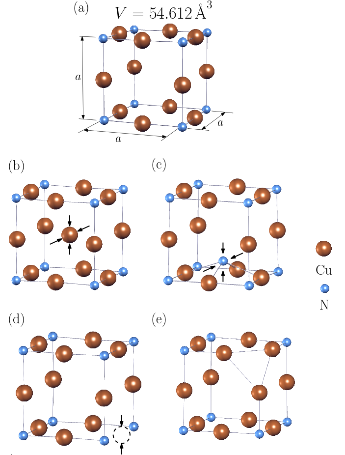
is a narrow gap semiconductor with multiple functional properties in bulk and thin film form, including solar energy conversion [28, 29], optical information storage, microelectronic semiconductors [22], and electronic devices [30, 31]. Cu3N has a cubic structure at room temperature (see Fig. 2(a)) and exhibits small direct and indirect optical gaps of 1.4 eV and 1.0 eV, respectively [32, 30, 31], high charge carrier mobilities (up to 200 cm2/Vs), and a high optical absorption coefficient of 105 cm-1 above 2 eV [33]. Cu3N thin films display bipolar -type and -type doping characteristics as a function of growth temperature and Cu/N flux ratio, enabling the fabrication of – junctions [32, 34]. The electronic structure of Cu3N exhibits anti-bonding and bonding characteristics at the valence and conduction edges, respectively, suggesting defect tolerance [32]. The large cavity of the body-centered cubic structure allows extrinsic doping with Ni [23], Ag, Au [24], Pd, In, Zn [35], Fe, Co, Ni [25], O [36], and Li [37].
Previous DFT work has investigated the defect properties of [30, 38, 33]. The conduction band minimum (CBM) and the valence band maximum (VBM) of are located at the M () and R () points, respectively, of the Brillouin zone [39, 40]. Cu and V display defect levels near the CBM and VBM, respectively [41, 40], supporting the observation of semiconductor transition. Antisite defects such as Cu and N exhibit high formation energies due to the significant electronegativity difference between Cu and N. The large Coulombic repulsion between the defects and the lattice renders the antisite defects inherently unstable [40, 31, 36].
Here, we focus on the formation energies of the thermodynamically stable intrinsic defects, evaluated under several supercell–size correction schemes. To that end, semilocal and hybrid density-functional calculations are combined with three complementary finite-size correction schemes to elucidate the – doping behavior of Cu3N. The corrected formation energies and charge-transition levels of intrinsic defects are evaluated under both N-rich and Cu-rich chemical potentials. Under N-rich growth conditions, charge neutrality is governed by VCu, Cui, and Ni, yielding -type conductivity, whereas in Cu-rich conditions, Cui becomes the most stable defect and drives -type conductivity. Because the spatial extent of these defects varies widely, no single size-correction approach is applicable to all cases. The finite-size correction methods developed here provide guidelines for choosing correction strategies when defect wave functions extend over multiple length scales, yielding dilute-limit energetics without excessive computational cost.
III Computational details
III.1 Electronic reference energies
Spin-polarized DFT calculations were performed using the Vienna Ab-initio Simulation Package (VASP) [42, 43]. We use the generalized gradient approximation of Perdew, Burke, and Ernzerhof (PBE) [44], supplemented by the Hubbard method [45] (PBE+), to describe the Cu orbitals more accurately. The Hubbard U value for the Cu states was set to 5 eV [30], using a plane-wave kinetic-energy cutoff of 400 eV and performing calculations at the -point. Core–valence interactions were treated with projector-augmented wave potentials that included 11 and 5 valence electrons for Cu and N, respectively [46]. Structures were relaxed within PBE+U until the maximum residual force was below 0.01 eV/Å. For cubic Cu3N, the optimized lattice constant is Å, in close agreement with the experimental value of 3.815 Å (deviation of 0.6%) [31].
Previous work has shown that semilocal functionals underestimate the optical band gap of Cu3N by [39, 47, 41]. By contrast, higher levels of theory, such as hybrid functionals [41, 40] and the GW approximation within many-body perturbation theory [41, 32], are able to reproduce the experimental optical gap [48, 32]. Consequently, defect formation energies were obtained from static total-energy calculations using the Heyd–Scuseria–Ernzerhof (HSE) hybrid functional [49, 50]. For Cu3N, the HSE band structure yields an indirect band gap of 0.93 eV in a supercell, with the gap located between the R and M points of the Brillouin zone (see Fig. S1 in Supplemental Material [51]). At the HSE (PBE+U) level, a supercell gives a gap of 0.92 eV (0.67 eV) when extracted from Kohn-Sham eigenvalues and 0.81 eV (0.57 eV) when extracted from total-energy differences between the neutral and charge states. These values are consistent with previous ab initio and experimental results [39, 41].

Previous work has shown that generalized Kohn–Sham eigenvalues obtained with HSE hybrid functionals can suffer from finite-size effects, leading to inaccurate band edge and band gap positions [52]. To ensure consistency with the defect-formation-energy formalism, we therefore determine the HSE band edges and band gap from the ionization potential and electron affinity of the pristine supercell (Fig. 3) [52]. Figure 3 compares the band edges obtained from two different methods as a function of supercell size for both the HSE and PBE+U functionals. The 256- and 864-atom supercells correspond to and multiples of the primitive cubic cell, respectively, whereas the 512-atom supercell has a rhombohedral shape. In method A, the band-edges are readily obtained as the CBM and VBM eigenvalues of the pristine supercell. In method B, the CBM and VBM are extracted from total energy differences between the neutral pristine supercell and supercells with one extra or one fewer electron, respectively. The two methods yield slightly different CBM and VBM positions. The origin of this residual discrepancy is not obvious, as the band-edges appear converged with respect to supercell size.
This shift could originate from the piecewise convexity of approximate density functionals [53]. However, it is surprising that this shift remains rather constant at 0.05-0.06 eV for PBE, PBE+U, and HSE functionals, the last of which is believed to mitigate this effect. Increasing the wavefunction cutoff to 625 eV does not modify this VBM shift, nor do other package-specific computational parameters.
III.2 Defects simulation
Intrinsic point defects in Cu3N were simulated using a supercell with a linear size , containing 256 atoms in the pristine case. The Brillouin zone of the supercell was sampled at a single -point, which avoids band filling errors and improves computational efficiency by enabling the use of real-valued linear-algebra routines. For supercells with even , the R and M points of the primitive Brillouin zone fold onto the supercell -point, so that the VBM and CBM are correctly captured in a single -point calculation. This folding does not occur for odd , as shown below, and single- calculations with odd-multiple supercells therefore fail to capture the true band-edge states and shallow defects. For this reason, all defect calculations reported here employ even-multiple supercells to ensure reliable sampling of the band edges. Materials with band extrema at k-points located away from the boundary of the first Brillouin zone, such as silicon, may require a distinct k-point for each supercell.
Formation energies and transition levels were computed by first relaxing the internal atomic coordinates with PBE+U and then performing a static HSE total-energy calculation on the PBE+U optimized structure. Charged defects were modeled by adding or removing electrons from the supercell, together with a compensating uniform background charge. In all cases, the supercell lattice parameter was kept fixed during the structural optimization to avoid spurious lattice and strain effects. This protocol, which combines PBE+U structural relaxation with HSE total energy calculations, substantially reduces the computational cost while preserving quantitative accuracy and qualitative trends for defect energetics.
Following Ref. [8], the formation energy of a defect with charge (in units of the elementary charge [54]) as a function of the Fermi level is given by
| (11) |
where and are the total energies of the defect supercell in charge state and the pristine supercell, respectively. The integers and the chemical potentials describe the exchange of atomic species with external reservoirs, with () for atoms added to (removed from) the supercell. The defect charge () corresponds to electrons added (removed), and is the electron chemical potential (Fermi level). It is convenient to express as
where is measured relative to the VBM of the pristine structure.
In plane-wave codes such as VASP, single-particle eigenvalues are referenced to the cell-averaged Hartree potential, which includes an arbitrary constant arising from the local parts of the PAW potentials. The potential-alignment term [Eq. (2)] corrects for the shift between the energy references of the defect and pristine supercells that results from adding or removing atoms and electrons, which changes the average Hartree potential. In Eq. (2), the quantity is interpreted as the number of electrons removed (consistent with Eq. (11)), while and denote the corresponding single-particle potential energies. In this convention, represents the shift of the potential-energy reference for single-particle levels and must be subtracted from the single-particle energies (e.g., in band diagrams) of the defect supercells. Finally, collects all remaining finite-size effects beyond potential alignment, which are discussed below.
To analyze the size dependence, we first compute the formation-energy contribution
| (12) |
using supercells () with a linear size . These size-scaling calculations are carried out at the PBE+U level, which allows us to treat larger supercells than are feasible with the HSE functional. Note that the VBM also shows a weak dependence on supercell size when only the -point is used; this effect is treated separately.
To determine the finite-size correction , the formation energies were computed within PBE+U (including ) for supercells with and a linear size . Defining
| (13) |
the quantity was analyzed as a function of and extrapolated to the limit. The extrapolated value,
| (14) |
was then added to the HSE formation energies obtained for the cell, assuming that the residual size error is independent of the functional. This procedure yields formation energies representative of the infinite-size limit while retaining the accuracy of the HSE functional. Our expression for the defect formation energy is
| (15) |

In Eq. (15), denotes the generalized Kohn–Sham eigenvalue of the highest occupied crystal orbital of the pristine supercell. Accordingly, is the Fermi level measured with respect to this VBM energy. Corrections to the VBM can be included by adding a term and modifying the Fermi level definition as , as illustrated in Fig. 4. Generally, the Fermi level takes values between the VBM and the CBM, i.e., within the forbidden band. The correction may change the stable charge states. In the schematic example of Fig. 4, the charge state is stable near , but after considering the correction of the VBM, the charge state is the only stable state. Similarly, corrections to the CBM can modify the stable charge states near the CBM. The quantity has three contributions: (1) the definition of the VBM as an ionization energy (see Fig. 3), (2) finite-size effects, and (3) quasiparticle corrections. The associated finite-size corrections are small (below 0.03 eV) and affect both VBM definitions and both functionals similarly. Quasiparticle corrections beyond the HSE level are not used in this work.
III.3 Thermodynamic constraints
Having established the electronic reference energies, we now specify the thermodynamic constraints on the atomic reservoirs. In thermodynamic equilibrium, the chemical potentials of the constituent elements and compounds must satisfy
| (16) |
It is convenient to express the elemental chemical potentials relative to their standard elemental references as
| (17) |
where is the chemical potential of the pure element in its stable phase and measures the deviation imposed by the growth environment (with the constraint ). The chemical potential of the compound is given by its total energy per formula unit,
| (18) |
where is the heat of formation. Combining Eqs. 5–7 yields the linear constraint
| (19) |
which defines the allowed range used in the defect formation-energy calculations.
The total energies of Cu3N and the competing phases (Cu, N) were computed at the HSE level to define consistent elemental chemical potentials and ensure phase stability (see Table 1). Cu3N is stable only within the range in which the competing phases are stable themselves, and the relationships described in Eqs. (16)–(19) are satisfied. Table S1 summarizes the reference elemental chemical potentials for Cu and N at the Cu-rich and N-rich limits, obtained from the total energies in Table 1. Gas-phase chemical potentials are related to the partial pressure through standard thermodynamic expressions. As Cu3N is metastable (see Ref. [38]), we adopt the quasi-thermodynamic chemical potential model, using solid Cu and dissociated N as references.
| System | (eV) | HSE Energy (eV) |
|---|---|---|
| Cu3N | -4.110 | -20.456 |
| Cu | 0.000 | -3.632 |
| N | 0.000 | -5.450 |
IV Results
IV.1 Analysis of size corrections fitting models
We discuss size corrections for low-energy intrinsic defects: (i) Cu interstitial (Cu), (ii) N interstitial (N), (iii) Cu vacancy (V), and N vacancy (VN). Figure 2 shows the lowest energy structure for the neutral case Cu (b), N (c), V (d), and V (e) after performing structural relaxations. The antisite defects CuN and NCu have large formation energies and are therefore not considered in this work [40]. In principle, interstitial defects can occupy multiple sites within the Cu3N cavity. However, previous studies have shown that Cu stabilizes at the center of the cubic Pmm structure, and we therefore initialized the structure in this configuration [40, 35, 24]. In contrast, for N, due to the small ion size of N, we consider multiple initial positions, including a tetragonal configuration of N bonded to three Cu ions and N in the corner; a diagonal N forming a plane with Cu atoms; and N near the center of the face of the unit cell, exhibiting corner placement towards the center of the cubic cavity. For V and V, we find that removing the Cu and N ions, respectively, induces negligible perturbation of the pristine structure.

For each charge defect, we computed the potential alignment correction (see Eq. (2)) for the charge defect energies. Figure 5 shows the potential average values in the defective supercell with respect to the reference values – those of the pristine supercell – as a function of the distance to the impurity or the vacancy center. Figures S2–S5 show the results for and supercells. The potential alignment was obtained as average values of the electrostatic potential in atomic spheres defined by the DFT code. These averages have a single value for each species, i.e., Cu or N, in the pristine supercell, but they vary across the defective supercell. The potential values are given multiplied by [54], hence these values are potential energies in eV units.
We find that the potential values are well converged to zero at large distance values, suggesting that the supercell is large enough to simulate an isolated impurity. As an estimation of the potential alignment correction, we used the value corresponding to the largest distance in the plot, multiplied by the defect charge . Most of the plots in Fig. 5 have the appearance of Coulomb pair potential energies, although they rather represent the interaction with a periodic array of defects imposed by the periodic boundary conditions. The cases of Cu and N are anomalous and will be discussed below.


Figure 6 presents finite size corrections to defect formation energies, obtained by extrapolating results from supercells () at the PBE+U level. The best fitting model is shown for each defect and charge state, and the discussion that follows provides support for the model selection. Other fitting models are shown in the Supplemental Material [51]. Table S2 shows the data used to obtain the size corrections by means of different fitting models. These data are the formation energy differences (Eq. (13)). Table 2 summarizes the size correction results and highlights the best value used to predict formation energies and defect levels in the last section.
IV.1.1 Interstitial copper defect Cu
Figure 6 reports finite size corrections to the formation energies of Cui for charge states . Figure S6 in the Supplemental Material [51] includes the Cu formation energy and compares two polynomial forms with the hydrogen-like model introduced earlier, which is the model shown in Fig. 6(a). Figure S6 shows an outlier at , corresponding to the formation energy computed with a supercell. This outlier demonstrates that odd supercells can yield anomalous values for the formation energy because they do not include the true VBM and CBM when only the -point is used. This effect has been observed in finite-size analysis of charged defects [55].
On the other hand, as the net charge is zero, the Makov-Payne monopole correction and the potential alignment do not explain the deviation trend with supercell size. Dipole or quadrupole corrections are also not expected because the impurity atoms are located in a centrosymmetric position. Therefore, we search for alternative fitting functions.
Figure 7 shows the band structure of pristine Cu3N and the neutral defect Cu, shown in panels (a) and (b), respectively, using the 4 4 4 supercell and the PBE+U functional in both cases. Since the formation energies are computed using single -point calculations, only the band energies at contribute to the calculated formation energy. Cu exhibits two in-gap bands with opposite spin and similar dispersion. Only one of the two levels at the -point is occupied, which explains the formation of the and charge states, as well as the values of the and transition levels.
Because the formation energies are computed using single -point calculations, the behavior of the bands at determines the accuracy of the fitting model. In the case of Cu, the shift of the -point energy from the band center is the primary cause of the size effect. The pronounced dispersion indicates interaction between periodic images of the defect. Therefore, using the hydrogen-like fitting model (see Eq. (9)), we obtain a formation energy correction of 0.17 eV. Figure S6 also shows that fitting the formation energies using polynomial functions, excluding the linear term, yields an extrapolated correction energy that is relatively close to that obtained with the hydrogen-like model.
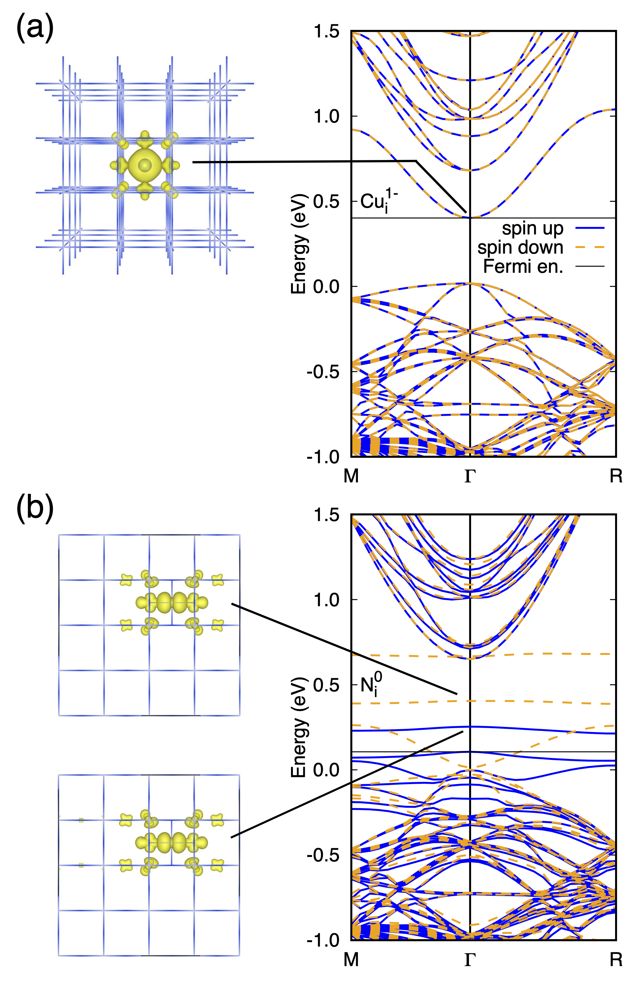
Additional insight can be obtained by considering the band diagram in the framework of the supercell. In order to reduce the computational cost, the bands were computed for the charge state , which allows a non-spin-polarized calculation. Figure 8(a) shows the bands for the Cu defect, which are nearly identical to the bands of the neutral state but are spin-degenerate. The latter is compared to the band diagram for the supercell shown in Fig. S7 (left panel), computed with only a few k-points to reduce the high computational cost. It can be noted that the in-gap band is narrower in the supercell than in the supercell, but the average band energy is practically the same, and it is very close to the CBM. Figure 8(a) also shows the interstitial atom at the supercell center, with an isosurface of the partial charge density (the square of the wavefunction) of the doubly occupied in-gap state of Cu. The decrease in bandwidth upon increasing the supercell size supports the idea that the bandwidth and the deep character of the in-gap level are size effects resulting from the interaction between the interstitial and its periodic replicas, and that Cu is a donor with shallow-like electronic character near the CBM. As will be shown below, the apparent deep character of the transition level is a size effect.
Figure S9 shows the formation energies and the fitted curves with the extrapolated values for Cu. According to the previous discussion, the impurity model was chosen as the best fitting model, providing a size correction of 0.33 eV. The enlarged value compared to the case of Cu is the result of the double occupation of the in-gap level. In principle, the Makov-Payne model could be applied to Cu, and this fit is also shown in Fig. S9, providing a size correction of 0.50 eV. However, the behavior of the core-averaged potential shown in Fig. 5(a) suggests the absence of a negatively point-like charge associated with the defect, which is also in agreement with the dispersive character of the in-gap band. Hence, we state that the Makov-Payne model is not appropriate to Cu.
| Defect | q | Rigid shift | Polynomial scaling | Impurity model |
|---|---|---|---|---|
| Cu | 0.16 | 0.18 | 0.17 | |
| 0.27 | 0.50 | 0.33 | ||
| -0.03 | 0.00 | -0.05 | ||
| N | 0.32 | 0.36 | 0.33 | |
| 0.29 | 0.37 | 0.31 | ||
| 0.39 | 0.50 | 0.41 | ||
| 0.25 | AN | AN | ||
| 0.17 | 0.36 | 0.23 | ||
| 0.19 | 0.25 | 0.20 | ||
| V | 0.10 | 0.13 | 0.11 | |
| 0.02 | 0.05 | 0.03 | ||
| V | 0.13 | 0.16 | NA | |
| 0.09 | 0.14 | NA | ||
| 0.07 | AN | NA | ||
| 0.14 | 0.14 | NA |
For the positive charge state, Cu, the monopole Makov-Payne correction may be appropriate, as the interstitial atom has lost its outer 4 electron and behaves as a positively charged point defect. The trend observed in the core-averaged electrostatic potential shown in Fig. 5(b) supports this interpretation. Figure S8 presents several fits using functions that include a monopole-type linear term along with a higher-order term. The choice for the best model is uncertain due to the fact that the data fall outside the linear convergence regime. However, in all cases, the extrapolated corrections are very small (0.02, 0.0, and -0.01 eV) and are well below the accuracy of DFT calculations. We adopt the intermediate value of 0.0 eV, obtained from fitting the function , which is consistent with the Makov-Payne formalism. This fitting is shown in Fig. 6(b). The fact that is consistent with the Makov-Payne model, as discussed in Sec. I.
IV.1.2 Deep N defect
The most stable position of interstitial nitrogen is located near the center of the unit cell face, coordinated with four Cu atoms, as shown in Fig. 2(c). The vertical displacement of the defect from the cell face varies with the defect charge. The band structure of N exhibits several in-gap bands, the character of which is clarified by the partial charge density at the -point shown in Fig. 8(b) for the supercell. The corresponding squared wave functions are strongly localized around the interstitial site and the neighboring atoms.
For N, Fig. S10 shows the formation energies of the neutral charge state and its fits with two models. First, a model that considers dipole-dipole interactions () plus residual interactions, and second, the hydrogenic impurity model used for Cu. Both models provide nearly the same correction; we chose the impurity model, also in Fig. 6(d), which has a correction of 0.33 eV. This rather large size correction is surprising. For N, the calculated electronic structure shows a clear size dependence. In the 4×4×4 supercell, the band diagram of Fig. 8(b) shows a spin down dispersive band crossing the Fermi energy and several non-dispersive bands near the Fermi energy, whereas in larger supercells (see Fig. S7) the bandwidth is reduced and the relative band ordering changes. This indicates that the residual size effect arises from defect-band dispersion, wavefunction overlap, and other interactions between periodic images, rather than from monopole electrostatics. Together with the Cu defect discussed earlier, this underlines the need to apply size corrections to the neutral defect formation energy.
For N, core average potentials and band diagrams suggest that the monopole correction must be present in the fitting model. However, the interaction is not isotropic, as seen in Fig. 5(d), where the core potential energies depend not only on the distance to the impurity. Also, the orbitals have different symmetries. Among the models, the case with is the only one that exhibits a dominant monopole character at large supercell sizes (see Fig. S11). We therefore select the model, also shown in Fig. 6(e), which yields a correction of 0.37 eV. Most of the alternative models produce corrections close to 0.35 eV, with the exception of the model, which deviates significantly.
Figure S12 shows the formation energies and the fitted curves with the extrapolated values for N. Similar to the previous case N, we choose the model (also in Fig. 6(f)) that gives a correction of 0.50 eV. For N, the extrapolation of total energy corrections is given in Fig. S13. Again, we choose the model (also in Fig. 6(g)) that gives a correction of 0.36 eV. For N, Fig. S14 shows the least squares fits for the models considered. In this case, the size dependence is anomalous, and the extrapolated energies are unreliable. Note that the dominant monopole correction should be given by , but all models give a correction with the opposite sign. Hence, we propose the correction as the difference between the and the calculations, i.e., 0.25 eV. The defect N has two electrons at the CBM, causing it to be unstable for all values of the Fermi level. Figure S15 shows the size dependence of the formation energy. The model is the best behaved, giving a size correction of 0.25 eV.
IV.1.3 Shallow V defect
The neutral V defect exhibits negligible lattice distortion, with Cu–N bond lengths of 1.90 Å varying by no more than 0.03 Å. Its band structure does not show any in-gap states (see Fig. 7(d)). The neutral configuration is non-magnetic within the PBE+U formalism. A spin-polarized calculation with a total spin of 1 yields an energy that is 0.01 eV higher than that of the spin-unpolarized case. There is a delocalized hole state at the VBM, which allows the charge state to adopt a closed-shell configuration and lowers its formation energy.
Figure S16 shows several fitting models applied to V, excluding monopole corrections. We select the model, which yields a size correction of 0.13 eV. For the charged state V, the least-squares fits are presented in Fig. S17. The Makov-Payne function model fits the size dependence, providing a size correction 0.05 eV. Other linear models, i.e., and , give the same correction, showing that the linear term is dominant.
IV.1.4 Shallow V defect
The nitrogen vacancy is shown in Fig. 2(e). In the neutral state, the neighboring Cu atoms move 0.137 Å towards the vacancy center, and their bond length with the next N atoms increases to 1.952 Å, a variation of 0.056 Å from 1.897 Å far from the vacancy. No in-gap levels are created, as shown in Fig. 7(c) for the neutral charge state V. The electronic structure of V is not spin-polarized, although the CBM is occupied by one electron. The state V has a closed shell configuration and is almost identical to the band diagram of V, as seen in Fig. S18. Both band diagrams show three bands with a non-dispersive character in the range 0.2-0.3 eV over the CBM. This feature indicates the presence of unoccupied localized vacancy levels. An HSE band-structure calculation shows the same behavior, as shown in Fig. S18.
Figures S19–S22 show the fitting curves of the formation energies of V for . For the neutral state, we have chosen the model with only cubic and quartic terms, giving a size correction of 0.16 eV. For V, the linear-cubic model gives a size correction of 0.14 eV. For V, the linear-cubic model gives , which contradicts the Makov-Payne model. Therefore, we have chosen the size correction as the difference between the formation energies of and results. Let us note that the cubic-quartic model gives almost the same corrections.
IV.2 Formation energies and defect level properties of Cu3N
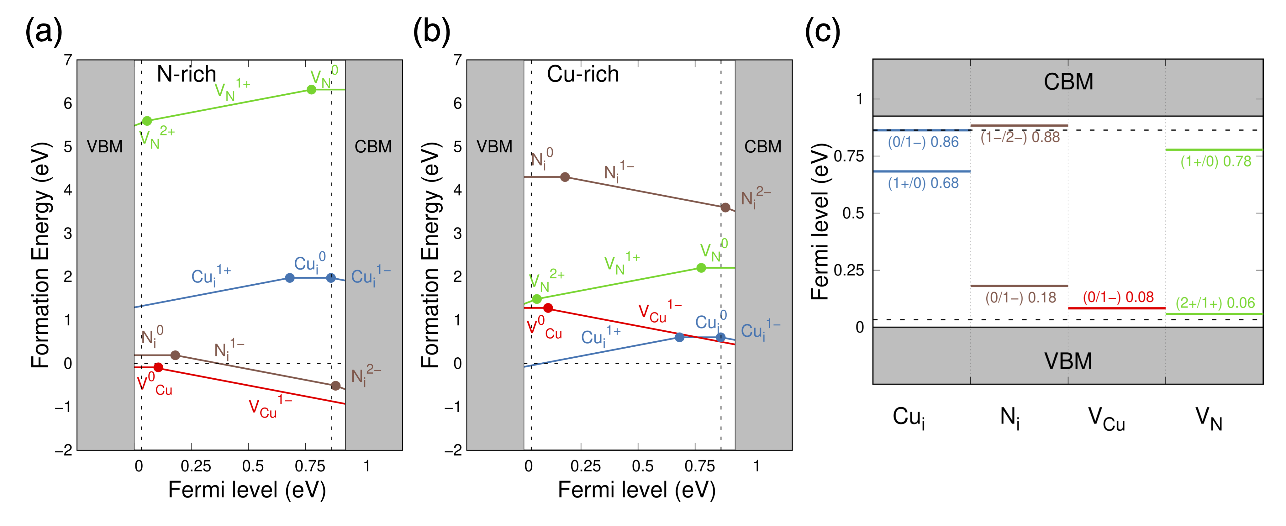
Having computed the finite-size corrections, we next evaluate the formation energies and defect levels. Figures 9(a) and (b) show the formation energies of Cu3N as a function of the Fermi level for N-rich and Cu-rich conditions, respectively. The results incorporate the finite-size corrections; the adopted values are highlighted in boldface in Table 2. Under N-rich conditions, the nitrogen vacancy V also has a relatively high formation energy and is thus unlikely to influence the bulk electrical properties. Its formation energy decreases under Cu-rich conditions, but it is still larger than for VCu and Cui. Therefore, V does not act as an effective source of free carriers.
Figure 9(c) summarizes the transition levels. The three low-energy defects (Cui, Ni, and VCu) exhibit distinct behavior: Cui acts as a donor with a (1+/0) transition level within eV of the CBM; but it is also an acceptor with the transition level resonant with the CBM. VCu behaves as a shallow acceptor with a level near the VBM; whereas Ni forms deeper and more strongly localized electronic states, in line with previous reports [41, 40]. Consistent with the charge-neutrality analysis, Cu3N is -type under N-rich conditions (stabilization of V and N) and -type under Cu-rich conditions (stabilization of Cu).
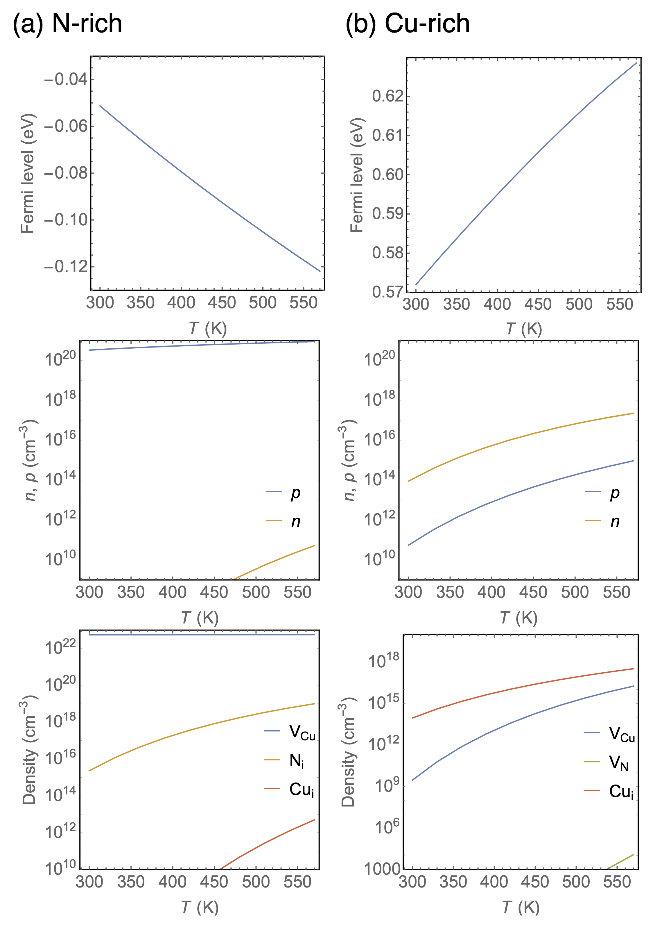
To analyze the or character of the material, we have determined the Fermi level by solving the charge-neutrality equation (CNE) [8] as a function of temperature (), as described in the Supplemental Material [51]. For N-rich conditions, the low-energy defects are exclusively the acceptor defects, Ni and VCu. Therefore, charge neutrality can be achieved between the holes and the negatively charged defects, suggesting a Fermi level between the transition level and the VBM, or even below the VBM. The numerical solution of the CNE, shown in Fig. 10(a), gives values between -0.05 and -0.12 eV for temperatures between 300 K and 570 K, respectively. The defect density, assumed to be in thermal equilibrium, is dominated by VCu in a concentration of , and a high hole density of . This represents an extreme case of heavy self-doping, as well as instability of the material, but it illustrates that strong -character can be achieved with N-rich conditions. Under Cu-rich conditions V, V and Cu have the lowest formation energies, which intersect in the range of 0.68-0.76 eV, pushing the Fermi level toward this range. Solving the CNE, we obtain Fermi level values between 0.57 and 0.63 eV, as shown in Fig. 10(b). As expected, the defect densities of Cui and VCu prevail, with values as large as for Cui at high temperatures. The electron density, , takes values between and cm-3, which is significantly smaller than the hole concentration, , under N-rich conditions. This stems from higher defect formation energies, leading to lower defect concentrations, along with the compensating effect of VCu.
V Conclusions
In summary, we have performed DFT total energy calculations of formation energies and transition levels for intrinsic point defects in Cu3N. The PBE+U method was employed to perform structural relaxations, while the HSE method was used to improve the total energies. The formation energies were corrected for potential alignment and size effects. For each defect and each charge state, the size corrections were obtained by extrapolating the defect formation energy computed with supercells of 256, 864, and 2048 atoms (pristine material). The extrapolation was obtained using a fitting model, which was selected for each defect.
The computed formation energies show that VCu acts as an acceptor near the VBM; Cui behaves as donor and resonant acceptor; and Ni (and VN when present) are associated with localized deep electronic states, consistent with prior reports. Our charge neutrality analysis yields -type behavior under N-rich conditions due to the stabilization of V at 0.08 eV, and -type behavior under Cu-rich conditions due to the stabilization of Cu at 0.68 eV.
We analyze explicit finite-size trends across a sequence of large supercells and determine which functional form best describes each defect according to its physical character. This allows us to identify cases in which conventional electrostatic scaling is adequate, as well as cases in which shallow character, defect-band dispersion, wavefunction overlap, or residual short-range interactions require more flexible defect-specific models.
Our work emphasizes that no universal finite-size correction applies across defect types. Different defects and defect states require different size correction methods or extrapolation strategies, and no single finite-size correction can be applied to all defect types. For Cu3N, we find that singly charged vacancies are accurately captured by Makov-Payne-type scaling (), while interstitial defects with shallow or weakly localized electronic character are better described by a hydrogenic impurity model that accounts for defect-band dispersion. Additionally, residual trends for neutral or weakly localized defects are best modeled by higher-order polynomial fits in and .
Overall, our results support an intrinsic – doping behavior of Cu3N under realistic chemical potentials and provide a practical, defect-specific protocol for assessing and correcting finite-size effects in semiconductors hosting both shallow and deep defects. Our strategy yields dilute-limit energetics at a practical computational cost and offers practical guidance for selecting correction schemes when defect wavefunctions span multiple length scales.
Acknowledgements.
A.M.R. acknowledges financial support from ANID Fondecyt Postdoctoral grant number 3220460. S.E.R.-L. acknowledges financial support from ANID Fondecyt Regular grant number 1260824. A.M.R. and S.E.R.-L. conducted theoretical work at The Molecular Foundry, which is supported by the Office of Science, Office of Basic Energy Sciences of the U.S. Department of Energy under contract No. DE-AC02-05CH11231. E.M.-P. thanks the computing time provided by the Servicio de Supercomputación de la Universidad de Granada (https://supercomputacion.ugr.es). Powered@NLHPC: This research was partially supported by the supercomputing infrastructure of the NLHPC (CCSS210001). The data that support the findings of this article are openly available at Ref. [56].Author Contributions
A.M.R.: formal analysis, funding acquisition, investigation, visualization, and writing the original draft. S.E.R.-L.: conceptualization, funding acquisition, resources, visualization, and supervision. E.M.-P.: data curation, formal analysis, methodology, resources, and visualization. All authors contributed to the investigation and the writing, review, and editing of the final manuscript.
References
- Zheng et al. [2021] Y. Zheng, T. J. Slade, L. Hu, X. Y. Tan, Y. Luo, Z. Z. Luo, J. Xu, Q. Yan, and M. G. Kanatzidis, Defect engineering in thermoelectric materials: what have we learned?, Chem. Soc. Rev. 50, 9022 (2021).
- Zhang et al. [2021] Q. Zhang, A. T. Wee, Q. Liang, X. Zhao, and M. Liu, Defect engineering of two-dimensional transition-metal dichalcogenides: Applications, challenges, and opportunities, ACS Nano 15, 2165 (2021).
- Seebauer and Noh [2010] E. G. Seebauer and K. W. Noh, Trends in semiconductor defect engineering at the nanoscale, Mater. Sci. Eng. R 70, 151 (2010).
- Ran et al. [2020] L. Ran, J. Hou, S. Cao, Z. Li, Y. Zhang, Y. Wu, B. Zhang, P. Zhai, and L. Sun, Defect engineering of photocatalysts for solar energy conversion, Sol. RRL 4, 1900487 (2020).
- Wang et al. [2018] F. Wang, S. Bai, W. Tress, A. Hagfeldt, and F. Gao, Defects engineering for high-performance perovskite solar cells, npj Flex. Electron. 2, 22 (2018).
- Bai et al. [2018] S. Bai, N. Zhang, C. Gao, and Y. Xiong, Defect engineering in photocatalytic materials, Nano Energy 53, 296 (2018).
- Zhang et al. [2020] Y. Zhang, L. Tao, C. Xie, D. Wang, Y. Zou, R. Chen, Y. Wang, C. Jia, and S. Wang, Defect engineering on electrode materials for rechargeable batteries, Adv. Mater. 32, 1905923 (2020).
- Freysoldt et al. [2014] C. Freysoldt, B. Grabowski, T. Hickel, J. Neugebauer, G. Kresse, A. Janotti, and C. G. Van De Walle, First-principles calculations for point defects in solids, Rev. Mod. Phys. 86, 253 (2014).
- Alkauskas et al. [2011] A. Alkauskas, P. Deák, J. Neugebauer, A. Pasquarello, and C. G. V. de Walle, Advanced calculations for defects in materials: Electronic structure methods (Wiley, 2011).
- Lambrecht [2011] W. R. Lambrecht, Which electronic structure method for the study of defects: A commentary, Phys. Status Solidi B 248, 1547 (2011).
- Walsh [2021] A. Walsh, Correcting the corrections for charged defects in crystals, npj Comput. Mater. 7, 72 (2021).
- Makov and Payne [1995] G. Makov and M. C. Payne, Periodic boundary conditions in ab initio calculations, Phys. Rev. B 51, 4014 (1995).
- Dabo et al. [2008] I. Dabo, B. Kozinsky, N. E. Singh-Miller, and N. Marzari, Electrostatics in periodic boundary conditions and real-space corrections, Phys. Rev. B 77, 115139 (2008).
- Freysoldt et al. [2009] C. Freysoldt, J. Neugebauer, and C. G. Van De Walle, Fully ab initio finite-size corrections for charged-defect supercell calculations, Phys. Rev. Lett. 102, 016402 (2009).
- Lany and Zunger [2008] S. Lany and A. Zunger, Assessment of correction methods for the band-gap problem and for finite-size effects in supercell defect calculations: case studies for ZnO and GaAs, Phys. Rev. B 78, 235104 (2008).
- Kumagai and Oba [2014] Y. Kumagai and F. Oba, Electrostatics-based finite-size corrections for first-principles point defect calculations, Phys. Rev. B 89, 195205 (2014).
- Lany et al. [2008] S. Lany, H. Raebiger, and A. Zunger, Magnetic interactions of Cr-Cr and Co-Co impurity pairs in ZnO within a band-gap corrected density functional approach, Phys. Rev. B 77, 241201 (2008).
- Komsa et al. [2012a] H.-P. Komsa, T. T. Rantala, and A. Pasquarello, Finite-size supercell correction schemes for charged defect calculations, Phys. Rev. B 86 (2012a).
- Komsa et al. [2012b] H.-P. Komsa, T. T. Rantala, and A. Pasquarello, Comparison between various finite-size supercell correction schemes for charged defect calculations, Physica B 407, 3063 (2012b).
- Kokott et al. [2018] S. Kokott, S. V. Levchenko, P. Rinke, and M. Scheffler, First-principles supercell calculations of small polarons with proper account for long-range polarization effects, New J. Phys. 20, 033023 (2018).
- Durrant et al. [2018] T. R. Durrant, S. T. Murphy, M. B. Watkins, and A. L. Shluger, Relation between image charge and potential alignment corrections for charged defects in periodic boundary conditions, J. Chem. Phys. 149, 024103 (2018).
- Jiang et al. [2018] A. Jiang, M. Qi, and J. Xiao, Preparation, structure, properties, and application of copper nitride (Cu3N) thin films: A review, J. Mater. Sci. Technol. 34, 1467 (2018).
- Lindahl et al. [2018] E. Lindahl, M. Ottosson, and J. O. Carlsson, Doping of metastable Cu3N at different Ni concentrations: growth, crystallographic sites and resistivity, Thin Solid Films 647, 1 (2018).
- Lu et al. [2013] N. Lu, A. Ji, and Z. Cao, Nearly constant electrical resistance over large temperature range in Cu3N ( Cu, Ag, Au) compounds, Sci. Rep. 3, 3090 (2013).
- Yang et al. [2014] J. Yang, S. Huang, Z. Wang, Y. Hou, Y. Shi, J. Zhang, J. Yang, and X. Li, Synthesis of copper nitride films doped with , , or by reactive magnetron sputtering, J. Vac. Sci. Technol. A 32, 051510 (2014).
- Menéndez-Proupin and Orellana [2015] E. Menéndez-Proupin and W. Orellana, Tellurium vacancy in cadmium telluride revisited: size effects in the electronic properties, Phys. Status Solidi B 252, 2649 (2015).
- Kittel [2005] C. Kittel, Introduction to Solid State Physics, 8th ed. (John Wiley & Sons, Inc., 2005).
- Rodríguez-Tapiador et al. [2023a] M. I. Rodríguez-Tapiador, J. M. Asensi, M. Roldán, J. Merino, J. Bertomeu, and S. Fernández, Copper nitride: a versatile semiconductor with great potential for next-generation photovoltaics, Coatings 13, 1094 (2023a).
- Rodríguez-Tapiador et al. [2023b] M. I. Rodríguez-Tapiador, A. Jiménez-Suárez, A. Lama, N. Gordillo, J. M. Asensi, G. del Rosario, J. Merino, J. Bertomeu, A. Agarwal, and S. Fernández, Effects of deposition temperature and working pressure on the thermal and nanomechanical performances of stoichiometric Cu3N: An adaptable material for photovoltaic applications, Nanomaterials 13, 2950 (2023b).
- Fioretti et al. [2016] A. N. Fioretti, C. P. Schwartz, J. Vinson, D. Nordlund, D. Prendergast, A. C. Tamboli, C. M. Caskey, F. Tuomisto, F. Linez, S. T. Christensen, E. S. Toberer, S. Lany, and A. Zakutayev, Understanding and control of bipolar self-doping in copper nitride, J. Appl. Phys. 119, 181508 (2016).
- Zervos et al. [2020] M. Zervos, A. Othonos, M. Sergides, T. Pavloudis, and J. Kioseoglou, Observation of the direct energy band gaps of defect-tolerant Cu3N by ultrafast pump-probe spectroscopy, J. Phys. Chem. C 124, 3459 (2020).
- Zakutayev et al. [2014] A. Zakutayev, C. M. Caskey, A. N. Fioretti, D. S. Ginley, J. Vidal, V. Stevanovic, E. Tea, and S. Lany, Defect tolerant semiconductors for solar energy conversion, J. Phys. Chem. Lett. 5, 1117 (2014).
- Matsuzaki et al. [2018] K. Matsuzaki, K. Harada, Y. Kumagai, S. Koshiya, K. Kimoto, S. Ueda, M. Sasase, A. Maeda, T. Susaki, M. Kitano, F. Oba, and H. Hosono, High-mobility -type and -type copper nitride semiconductors by direct nitriding synthesis and in silico doping design, Adv. Mater. 30, 1801968 (2018).
- Matsuzaki et al. [2014] K. Matsuzaki, T. Okazaki, Y. S. Lee, H. Hosono, and T. Susaki, Controlled bipolar doping in Cu3N (100) thin films, Appl. Phys. Lett. 105, 222102 (2014).
- Ji et al. [2010] A. Ji, D. Yun, L. Gao, and Z. Cao, Crystalline thin films of stoichiometric Cu3N and intercalated Cu3N ( metals): Growth and physical properties, Phys. Status Solidi A 207, 2769 (2010).
- Zervos et al. [2021] M. Zervos, A. Othonos, T. Pavloudis, S. Giaremis, J. Kioseoglou, K. Mavridou, M. Katsikini, F. Pinakidou, and E. C. Paloura, Impact of oxygen on the properties of Cu3N and Cu3-xN1-xOx, J. Phys. Chem. C 125, 3680 (2021).
- Wang et al. [2017] J. Wang, F. Li, X. Liu, H. Zhou, X. Shao, Y. Qu, and M. Zhao, and its analogs: a new class of electrodes for lithium ion batteries, J. Mater. Chem. A 5, 8762 (2017).
- Caskey et al. [2014] C. M. Caskey, R. M. Richards, D. S. Ginley, and A. Zakutayev, Thin film synthesis and properties of copper nitride, a metastable semiconductor, Mater. Horiz. 1, 424 (2014).
- Moreno-Armenta et al. [2007] M. G. Moreno-Armenta, W. L. Pérez, and N. Takeuchi, First-principles calculations of the structural and electronic properties of Cu3MN compounds with Ni, Cu, Zn, Pd, Ag, and Cd, Solid State Sci. 9, 166 (2007).
- Yee et al. [2018] Y. S. Yee, H. Inoue, A. Hultqvist, D. Hanifi, A. Salleo, B. Magyari-Köpe, Y. Nishi, S. F. Bent, and B. M. Clemens, Copper interstitial recombination centers in , Phys. Rev. B 97, 245201 (2018).
- Peng et al. [2013] H. Peng, D. O. Scanlon, V. Stevanovic, J. Vidal, G. W. Watson, and S. Lany, Convergence of density and hybrid functional defect calculations for compound semiconductors, Phys. Rev. B 88, 115201 (2013).
- Kresse and Furthmüller [1996a] G. Kresse and J. Furthmüller, Efficiency of ab initio total energy calculations for metals and semiconductors using a plane-wave basis set, Comput. Mater. Sci. 6, 15 (1996a).
- Kresse and Furthmüller [1996b] G. Kresse and J. Furthmüller, Efficient iterative schemes for ab initio total-energy calculations using a plane-wave basis set, Phys. Rev. B 54, 11169 (1996b).
- Perdew et al. [1996] J. P. Perdew, K. Burke, and M. Ernzerhof, Generalized gradient approximation made simple, Phys. Rev. Lett. 18, 3865 (1996).
- Dudarev and Botton [1998] S. Dudarev and G. Botton, Electron-energy-loss spectra and the structural stability of nickel oxide: An LSDA study, Phys. Rev. B 57, 1505 (1998).
- Kresse and Joubert [1999] G. Kresse and D. Joubert, From ultrasoft pseudopotentials to the projector augmented-wave method, Phys. Rev. B 59, 1758 (1999).
- Navío et al. [2007] C. Navío, M. J. Capitán, J. Álvarez, F. Yndurain, and R. Miranda, Intrinsic surface band bending in Cu3N (100) ultrathin films, Phys. Rev. B 76, 085105 (2007).
- Ebaid et al. [2020] M. Ebaid, D. M. Larson, K. C. Bustillo, J. H. Turner, and J. K. Cooper, Saw-tooth heat-cycling nitridation of metallic Cu yields first photoactive p-Cu3N for PEC applications, ACS Appl. Energy Mater. 3, 10714 (2020).
- Heyd et al. [2005] J. Heyd, G. E. Scuseria, and M. Ernzerhof, Hybrid functionals based on a screened Coulomb potential, J. Chem. Phys. 118, 8207 (2005).
- Krukau et al. [2006] A. V. Krukau, O. A. Vydrov, A. F. Izmaylov, and G. E. Scuseria, Influence of the exchange screening parameter on the performance of screened hybrid functionals, J. Chem. Phys. 125, 224106 (2006).
- [51] See Supplemental Material at https://journals.aps.org/authors/supplemental-material-instructions for additional Tables and Figures.
- Bang et al. [2013] J. Bang, Y. Y. Sun, T. A. Abtew, A. Samanta, P. Zhang, and S. B. Zhang, Difficulty in predicting shallow defects with hybrid functionals: implication of the long-range exchange interaction, Phys. Rev. B 88, 035134 (2013).
- Mori-Sánchez et al. [2008] P. Mori-Sánchez, A. J. Cohen, and W. Yang, Localization and delocalization errors in density functional theory and implications for band-gap prediction, Phys. Rev. Lett. 100, 146401 (2008).
- Millikan [1913] R. A. Millikan, On the elementary electrical charge and the Avogadro constant, Phys. Rev. 2, 109 (1913).
- Castleton et al. [2009] C. W. M. Castleton, A. Höglund, and S. Mirbt, Density functional theory calculations of defect energies using supercells, Modelling Simul. Mater. Sci. Eng. 17, 084003 (2009).
- Reyes et al. [2026] A. M. Reyes, S. E. Reyes-Lillo, and E. Menéndez-Proupin, Density functional theory calculations of intrinsic defects in Cu3N [data set], http://doi.org/10.5281/zenodo.18071017 (2026).