Dual-Polarization Quasi-BIC Refractive Index Sensing via Dielectric Symmetry Breaking in TiO2-BeS Metasurfaces Thanks: Preprint: Submitted to Optics Express.
Abstract
A dual-polarization dielectric metasurface sensor based on TiO2 nanobar pairs with a 20 nm BeS gap insert is numerically investigated in the near-infrared. The BeS layer introduces dielectric symmetry breaking without requiring geometric asymmetry, enabling polarization-selective excitation of two distinct resonances. Under TE illumination, the structure supports a quasi-BIC resonance at 879.2 nm with , whereas TM excitation produces a broader magnetic dipole resonance at 910.8 nm with . The spectral separation between the two modes enables simultaneous tracking of both polarization channels within a single measurement window. For background refractive indices from 1.00 to 1.05, the TE and TM resonances exhibit sensitivities of 243.1 and 178.8 nm/RIU, respectively. The corresponding figures of merit reach 35 and 7 RIU-1, with detection limits on the order of RIU. Field distributions show strong confinement of the TE mode inside the gap region, leading to enhanced overlap with the surrounding analyte. Because the two resonances respond differently to refractive-index variations, the metasurface produces a polarization-dependent spectral fingerprint that may provide additional selectivity beyond conventional single-channel dielectric sensors. The proposed platform further shows good tolerance against dimensional variation and consistent resonance behavior across independent FDTD solvers.
Keywords dielectric metasurface quasi-BIC refractive index sensing polarization multiplexing TiO2 BeS near-infrared
1 Introduction
Surface plasmon resonance (SPR) sensors remain widely used for label-free refractive index sensing because of their strong surface field confinement and high spectral sensitivity [19]. However, Ohmic loss in the metal layer broadens the resonance linewidth and limits the achievable quality factor [53, 44]. Local heating effects can also become problematic for biological analytes under certain operating conditions.
All-dielectric metasurfaces provide an alternative route for low-loss refractive index sensing by supporting electric and magnetic Mie resonances in high-index dielectric nanostructures [13, 29, 12, 9, 51, 26]. Silicon and TiO2 metasurfaces can support resonances with quality factors ranging from to without the absorption losses associated with metallic structures. In particular, quasi-bound states in the continuum (quasi-BICs) have attracted considerable attention because weak symmetry breaking can introduce controlled radiative coupling into otherwise dark modes [20, 27, 23, 31, 56, 46, 55, 49]. The resulting perturbation strength strongly influences both the resonance linewidth and coupling efficiency, making it an important design parameter in quasi-BIC metasurfaces.
Most dielectric refractive index sensors rely on a single spectral resonance shift as the sensing observable [28, 7, 46, 45]. As a result, different analytes can produce similar responses when their effective refractive indices are close. Additional sensing channels are therefore desirable, particularly for surface-sensitive measurements and multidimensional optical detection. Dual-resonance metasurfaces have been explored for this purpose because different resonant modes can exhibit distinct spatial field distributions and analyte overlap [46, 45]. Among the available approaches, polarization multiplexing provides a relatively simple implementation in which TE and TM illumination excite spectrally separated resonances within the same metasurface geometry [3].
TiO2 is well suited to this operating regime. Its refractive index – near 900 nm supports strong Mie resonances, its absorption edge near 350 nm keeps it transparent through the visible and near-infrared, and ALD deposits films with angstrom-level thickness control patternable by EBL to nm [40, 17, 36]. Reported TiO2 metasurface sensors reach 82–185 nm/RIU at factors of several thousand [48, 1]. Silicon absorbs below 1100 nm and cannot be used at the 879–911 nm resonances of the present design, making TiO2 the practical choice for this wavelength range.
The symmetry-breaking element introduced here is a 20 nm BeS bar placed inside the gap between each TiO2 nanobar pair. BeS is a II–VI semiconductor with an indirect bandgap near 5.4 eV [4]. In thin-film form, the broken out-of-plane symmetry of the zinc-blende lattice lifts the degeneracy of the principal dielectric tensor components and introduces a birefringence – at 900 nm [4, 52]. Both extinction coefficients are negligibly small across the near-infrared, so the insert is effectively lossless. The TE and TM fields therefore sample the gap region with different effective permittivities, which lifts the resonance degeneracy of the two bar-pair modes and produces two spectrally separated sensing channels from a single geometry. First-principles calculations further show that molecular adsorption modifies the BeS optical constants along each crystallographic axis in an analyte-specific way [52], which points toward chemical discrimination in a future experimental extension of this work.
We numerically show that a single 20 nm BeS bar inside the TiO2 nanobar-pair gap activates a quasi-BIC resonance under TE illumination and a magnetic dipole mode under TM illumination, with no geometric asymmetry required. FDTD simulations establish the sensing metrics of both channels. Near-field maps connect the sensitivity difference between channels to the spatial distribution of the modal energy. A two-dimensional polarization fingerprint shows what a dual-channel readout can resolve that a single-resonance sensor cannot. Structural tolerance sweeps, BeS optical-constant perturbation tests, and cross-platform validation against the Tidy3D solver confirm the numerical robustness of the results.
2 Structure and Simulation Method
2.1 Device geometry
The unit cell is shown in Fig. 1. Two TiO2 nanobars of width nm, length nm, and height nm are separated by a gap of nm along . A BeS bar of thickness 20 nm sits symmetrically inside this gap. The unit cell period along is nm. The structure rests on a SiO2 substrate (), and the superstrate is the analyte medium of index .
TiO2 optical constants come from the ALD-film ellipsometry data of Siefke et al. [40], giving with negligible extinction at 800–950 nm. SiO2 dispersion follows Kischkat et al. [25]. The BeS directional constants (, , , ) are from first-principles calculations for pristine BeS [39]. Both components are near zero at 800–1000 nm, so the insert is effectively lossless.

2.2 FDTD simulation details
All simulations used Lumerical FDTD [2] with periodic boundary conditions in and and perfectly matched layers (PML) in [5]. A broadband plane-wave source spanning 850–950 nm was incident along .
Separate campaigns covered 0∘ polarization ( along , across the gap) and 90∘ polarization ( along , along the bar axis). A non-uniform conformal mesh with a minimum cell size of 5 nm was used. Mesh convergence was checked by comparing 10 nm and 5 nm meshes; the resonance wavelength shifted by only nm (Fig. 2), negligible compared to the RI-induced shift of 12 nm per 0.05 RIU. Each run was continued until the stored field energy fell below of its peak value, which is standard practice for accurate linewidth extraction [54, 43].

Transmission was recorded by a frequency-domain power monitor placed above the structure and normalized to a reference run without any nanostructure. Resonance wavelengths and linewidths were extracted by fitting the transmission dip to the Fano lineshape [33, 34],
| (1) |
where is the off-resonance background transmission, is the Fano asymmetry parameter, is the resonance wavelength, and is the full width at half maximum (FWHM). The quality factor is . Both resonances exhibit asymmetric lineshapes arising from interference between the narrow resonant mode and the broad radiation continuum, a hallmark of quasi-BIC coupling that is well described by the Fano formula [24, 27, 23]. Sensitivity was extracted from a linear fit to over – in steps of 0.01 (12 FDTD runs total). The figure of merit is FOM [47] and the limit of detection is LoD , assuming a 0.01 nm wavelength resolution [41].
3 Results
3.1 BeS crystal structure and optical constants
3.1.1 Crystal structure
Bulk BeS crystallizes in the zinc-blende (sphalerite) structure with space group (No. 216) [21]. Each Be2+ cation is tetrahedrally coordinated by four S2- anions with a Be–S bond length of 2.11 Å. The cubic symmetry of the bulk phase means that the three principal dielectric tensor components are degenerate in the unstrained crystal. However, when BeS is grown as an ultrathin film or monolayer on a planar substrate, the broken out-of-plane symmetry lifts this degeneracy and introduces a measurable birefringence [22, 52]. It is this thin-film birefringence that is exploited in the present design: the 20 nm BeS bar presents different permittivities to the TE (-polarized) and TM (-polarized) fields, lifting the resonance degeneracy of the two TiO2 bar modes.
3.1.2 DFT origin of the optical constants
The directional optical constants used in this work come from a comprehensive first-principles study of the BeS monolayer and its interaction with volatile organic compounds (VOCs) [39]. DFT calculations used the GGA-PBE exchange-correlation functional [35] together with the Grimme dispersion correction [18] on a BeS supercell with a 21 Å vacuum slab. The relaxed pristine monolayer has a lattice constant of 3.459 Å, a Be–S bond length of 1.993 Å, a bond angle of 120∘, and a DFT-PBE band gap of 4.529 eV, consistent with earlier theoretical reports [22, 52].
That same study found that adsorption of 4-hydroxyhexanal (4HHE), isoprene, propanal, benzene, acetone, CO2, and H2O each introduces mid-gap defect states on the BeS surface and alters the in-plane and out-of-plane optical constants in a way that is distinct for each analyte [39]. The present work uses only the pristine-BeS constants, which establish the baseline birefringence and the lossless character of the gap insert. The adsorbate-modified constants from Ref. [39] represent a ready, first-principles input dataset for extending the metasurface to analyte-specific optical gas discrimination, and that extension is left as a direct continuation of this work.
Fig. 3 shows the dispersive and of pristine BeS along and from 400 to 2000 nm. Across the 800–1000 nm sensing window, – and –, and both extinction coefficients remain below 0.005. The birefringence – is what causes the two polarizations to couple to the gap insert with different effective permittivities, and it is ultimately the physical origin of the spectral separation between the two sensing channels.
To our knowledge, no experimental near-infrared ellipsometry data exist for BeS thin films in the open literature. This uncertainty is addressed in Sec. 3.7 by running additional simulations with and each perturbed by from their DFT values.

3.2 Effect of the BeS insert
Fig. 4 compares the 0∘ transmission spectrum of the bare TiO2 bar pair (no BeS) with that of the BeS-loaded structure at . Without the insert the bar pair supports a symmetric resonance at 876.9 nm with a relatively broad lineshape. Adding the 20 nm BeS bar red-shifts the resonance by 2.3 nm to 879.2 nm and narrows the dip, as visible in the sharper descent on the long-wavelength side. The redshift originates from the increased effective index inside the gap region, while the linewidth reduction indicates modified radiative coupling introduced by the dielectric perturbation. Without the BeS insert, the antisymmetric mode remains weakly coupled to the radiation continuum because of the nearly symmetric bar-pair geometry. Introducing the gap insert breaks this symmetry and enables excitation of the quasi-BIC resonance observed in the loaded structure.

3.3 Transmission spectra and resonance physics
Figure 5 shows the transmission spectra of the metasurface for both polarizations at . The 0∘ (TE) response exhibits a narrow Fano resonance at nm, whereas the 90∘ (TM) channel supports a broader resonance at nm. The 31.6 nm spectral separation allows both resonances to be resolved within the same spectral window. Fano fits to the transmission spectra are shown in Fig. 6. The extracted asymmetry parameters are and , with corresponding fitting coefficients of and . The smaller linewidth of the TE resonance is consistent with weaker radiative leakage relative to the TM mode. The extracted FWHM values are nm and nm, giving quality factors of and .


The two resonances have distinct physical origins. The 0∘ resonance at 879.2 nm is a gap-coupled quasi-BIC mode. In a perfectly symmetric TiO2 bar pair, the antisymmetric superposition of the two bar dipole modes has opposing dipole moments that cancel in the far field, making it a symmetry-protected dark mode [20, 27]. The BeS bar breaks this symmetry dielectrically by introducing different permittivities along and in the gap region. This allows the dark mode to radiate, producing a quasi-BIC resonance with strong gap field confinement. The asymmetric Fano lineshape () arises directly from the interference between this narrow quasi-BIC mode and the broad radiation continuum [33, 24], and is the standard lineshape reported for quasi-BIC sensors with weak geometric or dielectric symmetry breaking [27, 23, 46].
The 90∘ resonance at 910.8 nm is a magnetic dipole (MD) mode driven by the -polarized field. The displacement current circulates inside the TiO2 bar cross-section, storing energy predominantly in the bar volume rather than in the gap [14, 42]. The map shows four lobes inside the bar, consistent with MD excitation (Fig. 8b). Because the BeS insert occupies only a small fraction of the MD mode volume, the analyte overlap integral is lower than for the gap mode [38, 37]. This explains why is 26% below .
3.4 Near-field electric-field distributions
Figs. 7 and 8 show the normalized and distributions at each resonance wavelength in the cross-section through the gap.
At the 0∘ resonance (Fig. 7a), the field is concentrated near the inner corners of the TiO2 bars close to the substrate interface, indicating strong gap-mode confinement. In contrast, the 90∘ resonance (Fig. 7b) exhibits a broader field distribution near the upper bar region (– nm), consistent with magnetic dipole localization inside the dielectric bars.

(a)

(b)
At the 0∘ resonance (Fig. 8a), forms a sharp vertical stripe at the gap center (), exactly where the BeS bar sits. This gap-confined hot spot confirms that the mode is directly sensitive to the permittivity of the gap region, and directly accounts for the higher sensitivity of the 0∘ channel. At the 90∘ resonance (Fig. 8b), shows four lobes arranged symmetrically inside the bar, the characteristic quadrupolar signature of an MD mode oriented along the bar axis [42, 13]. The gap field is noticeably weaker here, consistent with the lower sensitivity of this channel.

(a)

(b)
3.5 Refractive index sensing
Fig. 9 shows the resonance wavelength heat map as goes from 1.00 to 1.05. Both resonances red-shift monotonically with no mode crossings. Fig. 10 shows the extracted wavelengths with linear fits ( for both). The sensitivities are
| (2) | ||||
| (3) |
The 0∘ mode is more sensitive because its gap-confined field has a larger overlap with the analyte. A rise in shifts the effective index of the gap mode more than that of the MD mode, which stores energy mostly inside TiO2.


The full sensing metrics are summarized in Table 1 and Fig. 11. At a wavelength resolution of 0.01 nm, the 0∘ channel gives LoD RIU and the 90∘ channel gives LoD RIU.
| Polarization | (nm/RIU) | FWHM (nm) | FOM (RIU-1) | LoD (RIU) | ||
|---|---|---|---|---|---|---|
| 0∘ (TE) | 243.1 | 6.87 | 128 | 0.10 | 35.4 | |
| 90∘ (TM) | 178.8 | 25.55 | 36 | 0.25 | 7.1 |

3.6 Polarization fingerprint
Because the two resonances exhibit different refractive-index sensitivities, each value of maps to a distinct point in the parameter space. As shown in Fig. 12, the simulated RI values fall along a line with slope .
The polarization-dependent response originates from the different field distributions of the TE and TM resonances. Consequently, analytes with similar bulk refractive indices but different optical anisotropy or surface interaction may exhibit different ratios [28, 7]. The isotropic response slope is determined by the metasurface geometry and may additionally serve as an internal calibration reference [28].

3.7 Structural parameter sweeps and fabrication tolerance
The influence of geometric variation on the resonance response was investigated through parameter sweeps and fabrication-tolerance analysis. Figure 13 shows the dependence of on the principal structural parameters. Among the investigated dimensions, the resonance position is most sensitive to variations in bar height and unit-cell period, where a nm perturbation produces shifts of approximately 20–40 nm. The responses to gap-width and bar-width variation remain comparatively smaller. Because ALD processes routinely achieve thickness control near nm [40, 36], the resonance wavelength is expected to depend primarily on the deposition thickness.
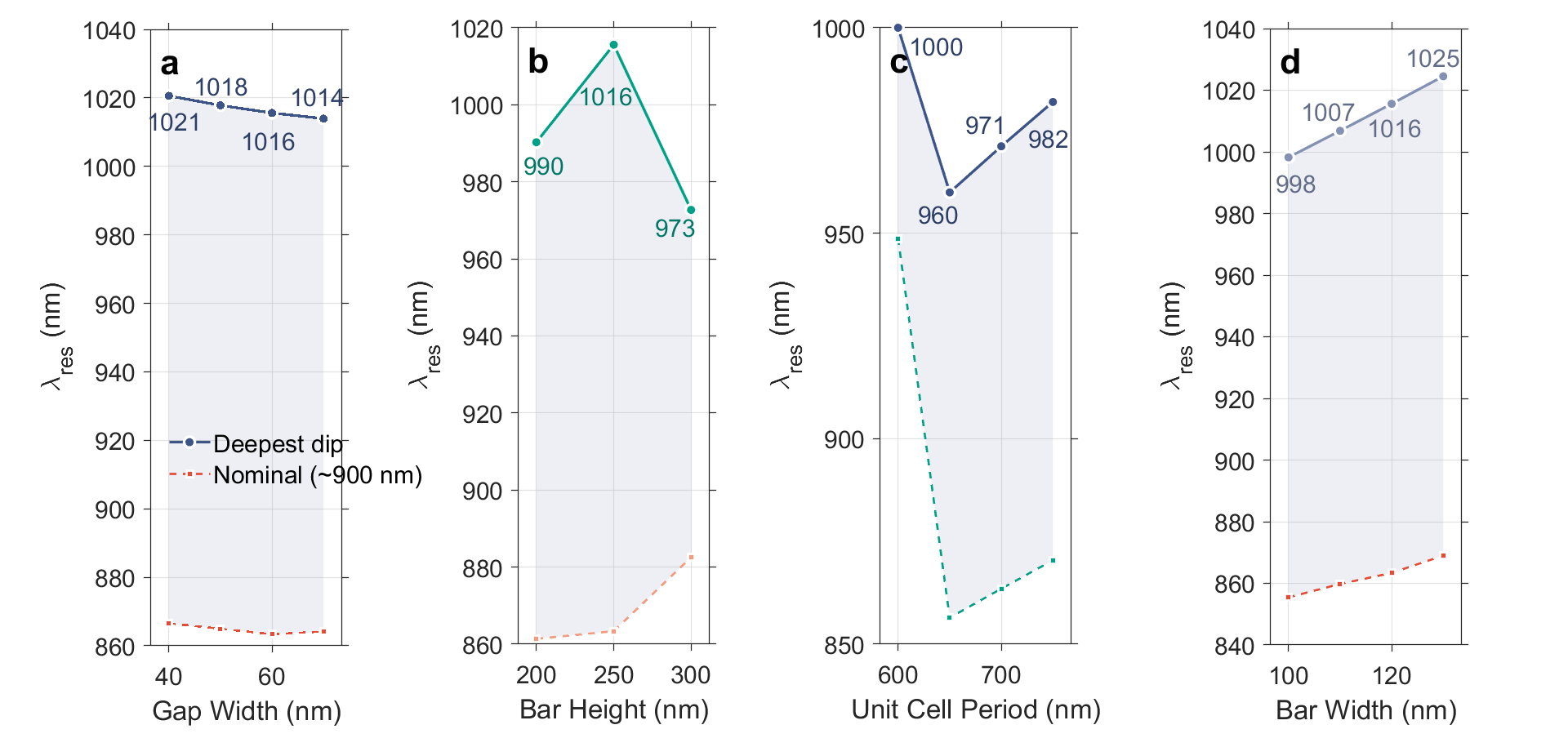
The combined influence of width and gap variation is summarized in Fig. 14. The nominal operating point ( nm, nm) lies close to a local minimum in the relative resonance-shift map, indicating partial compensation between correlated dimensional errors.

The effect of bar-length asymmetry was additionally examined to estimate sensitivity to EBL dose variation. As shown in Fig. 15, reducing from 450 to 440 nm (–) produces resonance shifts below 0.5 nm, indicating relatively weak sensitivity to moderate bar-length mismatch.

Figure 16 summarizes the overall fabrication tolerance through heatmaps of and for nm dimensional perturbations. Bar height and unit-cell period produce the largest variations in both resonance wavelength and quality factor.

Additional simulations were performed by varying both and by relative to their nominal DFT values. The resulting resonance shifts remain below 2.1 nm, while the corresponding variation in is less than 3%. These changes are small compared with the resonance shifts induced by refractive-index variation in the sensing range considered here.
Figure 17 compares the normalized sensing metrics for the two polarization channels. The TE resonance exhibits stronger sensitivity and figure of merit, whereas the TM resonance maintains comparatively higher robustness in linewidth-related performance.

3.8 Cross-platform FDTD validation
To assess the solver dependence of the resonance wavelengths, the nominal geometry was independently simulated using the Tidy3D finite-difference time-domain solver [15]. Tidy3D uses a cloud-based FDTD engine with a distinct grid implementation and perfectly matched layer formulation from Lumerical [5, 43]. The same unit cell dimensions, material constants, broadband source range (850–950 nm), and auto-shutoff criterion ( field energy decay) were applied in both solvers.
The Tidy3D resonance wavelengths are nm and nm, compared to 879.2 and 910.8 nm in Lumerical. The offsets are and nm for the two polarizations respectively. The near-identical magnitude of the offset across both polarization channels confirms that it arises from systematic mesh discretization rather than a physics disagreement between the two solvers. A systematic offset of this magnitude is consistent with prior cross-platform comparisons of dielectric metasurface resonators in this class [54, 16, 11].
Fig. 18 summarizes the cross-platform validation through four complementary views. The anchor-point agreement in panel (d) independently confirms that nm/RIU and nm/RIU are solver-independent.

(a)

(b)

(c)

(d)
4 Discussion
| Structure | (nm/RIU) | FOM (RIU-1) | (nm) | Dual | Ref. | |
| TiO2 GMR | 82 | 3208 | 433 | 800 | No | [48] |
| TiO2 multimodal | 185 | – | 210 | NIR | No | [1] |
| Si TD-EQ qBIC | 399 | 4959 | 1281 | NIR | No | [23] |
| Si dual-rod qBIC | 408 | – | 1823 | NIR | No | [10] |
| Si nanodisk qBIC | 440 | 9400 | 4223 | 980 | No | [56] |
| a-Si qBIC (Exp.) | 413 | – | 66 | NIR | No | [31] |
| Si dual-Fano qBIC | 529/347 | – | – | NIR | Yes | [46] |
| Si3N4 H-pillar BIC | – | – | – | NIR | Yes | [50] |
| Si H-disk TD qBIC | 262 | 2183 | NIR | No | [55] | |
| -qBIC | – | – | – | NIR | No | [49] |
| Si dual qBIC | – | 415 | – | NIR | Yes | [45] |
| TiO2 SOP (Exp.) | – | – | – | VIS | Yes | [28] |
| This work, 0∘ | 243 | 128 | 35 | 879 | Yes | |
| This work, 90∘ | 179 | 36 | 7 | 911 | Yes |
Table 2 places the present design among recently reported all-dielectric RI sensors, spanning single-channel and dual-channel designs over the 2020–2025 period.
The factors here (36–128) are substantially below quasi-BIC silicon designs reaching [23, 31, 56, 55]. The moderate factors are associated with the weak dielectric perturbation introduced by the BeS insert (–), which produces only limited radiative coupling of the quasi-BIC mode. The extracted Fano asymmetry parameters (–) are consistent with this behavior. The same perturbation-controlled trade-off is well documented in geometric asymmetry designs: larger asymmetry gives lower but broader spectral coverage and greater fabrication tolerance [56, 30]. A recent permittivity-asymmetric qBIC design by Yang et al. [49] takes a conceptually related approach of using dielectric rather than geometric asymmetry to activate the quasi-BIC, though with a different material system and sensing modality. The key advantage of the present design is not the absolute value but the dual-channel output and the NIR operating wavelength. None of the high- quasi-BIC designs in Table 2 provide two independent polarization channels. Wang et al. [46] achieve dual Fano channels in silicon with sensitivities of 529 and 347 nm/RIU, but through geometric rather than dielectric symmetry breaking, and without the analyte-specific detection pathway offered by the adsorbate-responsive BeS insert.
The conceptually closest prior work is the TiO2 state-of-polarization sensor of Kramadhati et al. [28], which is experimentally demonstrated but operates in the visible range. The near-infrared is more relevant for biosensing applications because many molecular absorption bands lie in the 700–1100 nm window [6, 32].
The sensitivities of 243 and 179 nm/RIU sit within the range reported for comparable TiO2 and moderate- silicon sensors [48, 1]. TiO2 is transparent from about 350 nm through the near-infrared, which makes it practical at the 879 and 911 nm resonances here. Silicon absorbs below about 1100 nm and cannot be used in this range [40, 17].
The 20 nm BeS insert has two roles. It sits at the gap field maximum and introduces directional permittivity that breaks the polarization degeneracy of the bar modes, playing the same role as the geometric parameter in prior asymmetric designs [8, 54]. It also responds to molecular adsorption through changes in and [52, 39], which a future version of this sensor can exploit for analyte-specific detection. The adsorbate optical constants computed in Ref. [39] for seven lung-disease biomarkers (4HHE, isoprene, propanal, benzene, acetone, CO2, H2O) on the BeS monolayer provide a ready, first-principles input dataset for such an extension.
This study is entirely computational. The TiO2 and SiO2 constants come from experimentally verified datasets [40, 25], and mesh convergence confirms numerical accuracy. Sidewall roughness and BeS film non-uniformity are not included in the model. The tolerance sweeps cover systematic dimensional errors but not stochastic roughness, which is left for future work.
5 Conclusion
A dual-polarization TiO2–BeS dielectric metasurface was numerically investigated for refractive index sensing in the near-infrared region. By introducing a thin BeS insert inside the TiO2 nanobar gap, the structure supports two polarization-dependent resonances. This eliminates the need for geometric asymmetry. Under TE illumination, the quasi-BIC resonance at 879.2 nm achieves a sensitivity of 243.1 nm/RIU and a quality factor of 128, while the TM magnetic dipole mode at 910.8 nm yields 178.8 nm/RIU with . The corresponding figures of merit are 35.4 and 7.1 RIU-1, with detection limits of and RIU respectively. The TE channel exhibits a quasi-BIC resonance with higher sensitivity, while the TM channel supports a broader magnetic dipole mode with a distinct spectral response.
The different refractive-index dependence of the two resonances produces a polarization-dependent spectral fingerprint. This can offer additional selectivity compared with conventional single-channel dielectric sensors. Because the two sensitivity values differ by 26%, isotropic analytes trace a fixed slope in the dual-channel shift space, while analytes with optical anisotropy or asymmetric surface interaction deviate measurably from this reference line, providing a discrimination capability unavailable from a single resonance. The all-dielectric TiO2/SiO2 platform is fully compatible with ALD deposition and electron-beam lithography, placing the structure within reach of current nanofabrication capabilities. Cross-platform simulations and fabrication-tolerance studies further reveal that the resonance behavior remains stable under moderate numerical and structural variation.
The present study is fully computational and does not include experimental uncertainties such as surface roughness or nonuniform BeS film formation. In addition, analyte-specific discrimination was not directly modeled using adsorbate-modified optical constants. Future work may extend the present platform toward experimentally realizable polarization-resolved sensing using analyte-dependent BeS optical responses and integrated microfluidic architectures. First-principles optical constants for seven biomarker adsorbates on BeS (4HHE, isoprene, propanal, benzene, acetone, CO2, and H2O) are already available [39], so this extension does not require additional DFT calculations.
Acknowledgments
The authors acknowledge the computational support and simulation resources utilized throughout this study.
Disclosures
The authors declare no conflicts of interest.
Data Availability
All key structural parameters and simulation conditions required to reproduce the reported results are provided within the manuscript. Additional simulation data are available from the corresponding author upon reasonable request.
References
- [1] (2020) Engineering multimodal dielectric resonance of TiO2 based nanostructures for high-performance refractive index sensing applications. Opt. Express 28 (16), pp. 23509–23522. External Links: Document Cited by: §1, Table 2, §4.
- [2] (2024) Lumerical FDTD solutions. Note: https://www.ansys.com/products/photonics/fdtd Cited by: §2.2.
- [3] (2015) Dielectric metasurfaces for complete control of phase and polarization with subwavelength spatial resolution and high transmission. Nature Nanotechnology 10, pp. 937–943. External Links: Document Cited by: §1.
- [4] (2021) Ground state properties of the wide band gap semiconductor beryllium sulfide (BeS). Materials 14 (20), pp. 6128. External Links: Document Cited by: §1, Figure 3.
- [5] (1994) A perfectly matched layer for the absorption of electromagnetic waves. J. Comput. Phys. 114 (2), pp. 185–200. External Links: Document Cited by: §2.2, §3.8.
- [6] (2023) Near-infrared spectroscopy for biomedical sensing and imaging: a review. J. Near Infrared Spectrosc. 31 (1), pp. 1–16. External Links: Document Cited by: §4.
- [7] (2026) Flatland metasurfaces for optical gas sensing. Sensors 26 (4), pp. 1293. External Links: Document Cited by: §1, §3.6.
- [8] (2016) Broken symmetry dielectric resonators for high quality factor Fano metasurfaces. ACS Photonics 3 (12), pp. 2061–2068. External Links: Document Cited by: §4.
- [9] (2016) A review of metasurfaces: physics and applications. Rep. Prog. Phys. 79 (7), pp. 076401. External Links: Document Cited by: §1.
- [10] (2024) Dual high- Fano resonances metasurface excited by asymmetric dielectric rods for refractive index sensing. Nanophotonics 13 (5), pp. 689–699. External Links: Document Cited by: Table 2.
- [11] (2026) Inverse design validation of Cs3Cu2Cl5-based microring resonator. Note: Tidy3D Community Library, https://www.flexcompute.com/tidy3d/community/notebooks/Cs3Cu2Cl5_MRR/ Cited by: §3.8.
- [12] (2015) High-efficiency dielectric Huygens’ surfaces. Adv. Opt. Mater. 3 (6), pp. 813–820. External Links: Document Cited by: §1.
- [13] (2012) Demonstration of magnetic dipole resonances of dielectric nanospheres in the visible region. Nano Lett. 12 (7), pp. 3749–3755. External Links: Document Cited by: §1, §3.4.
- [14] (2010) Optical response features of Si-nanoparticle arrays. Phys. Rev. B 82, pp. 045404. External Links: Document Cited by: §3.3.
- [15] (2024) Tidy3D: cloud-native FDTD electromagnetic solver. Note: https://www.flexcompute.com/tidy3d/ Cited by: §3.8.
- [16] (2023) High-Q silicon resonator. Note: Tidy3D Example Library, https://www.flexcompute.com/tidy3d/examples/notebooks/High_Q_Si_Resonator/ Cited by: §3.8.
- [17] (2021) Quasi-guided modes in titanium dioxide arrays fabricated via soft nanoimprint lithography. ACS Appl. Mater. Interfaces 13 (40), pp. 47860–47870. External Links: Document Cited by: §1, §4.
- [18] (2006) Semiempirical GGA-type density functional constructed with a long-range dispersion correction. Journal of Computational Chemistry 27 (15), pp. 1787–1799. External Links: Document Cited by: §3.1.2.
- [19] (2008) Surface plasmon resonance sensors for detection of chemical and biological species. Chem. Rev. 108 (2), pp. 462–493. External Links: Document Cited by: §1.
- [20] (2016) Bound states in the continuum. Nat. Rev. Mater. 1, pp. 16048. External Links: Document Cited by: §1, §3.3.
- [21] (2020-07) Materials data on BeS by the Materials Project. Note: Materials Project Database, entry mp-422https://next-gen.materialsproject.org/materials/mp-422 External Links: Document Cited by: §3.1.1.
- [22] (2016) Electronic and optical properties of beryllium sulfide monolayer: under stress and strain conditions. Physics Letters A 380 (42), pp. 3546–3552. External Links: Document Cited by: §3.1.1, §3.1.2.
- [23] (2023) High-sensitivity sensing in all-dielectric metasurface driven by quasi-bound states in the continuum. Nanomaterials 13 (3), pp. 505. External Links: Document Cited by: §1, §2.2, §3.3, Table 2, §4.
- [24] (2006) Classical analogy of Fano resonances. Phys. Scr. 74 (2), pp. 259–266. External Links: Document Cited by: §2.2, §3.3.
- [25] (2012) Mid-infrared optical properties of thin films of aluminum oxide, titanium dioxide, silicon dioxide, aluminum nitride, and silicon nitride. Appl. Opt. 51 (28), pp. 6789–6798. External Links: Document Cited by: §2.1, §4.
- [26] (2021) Dielectric resonant metaphotonics. ACS Photonics 8 (1), pp. 102–112. External Links: Document Cited by: §1.
- [27] (2018) Asymmetric metasurfaces with high- resonances governed by bound states in the continuum. Phys. Rev. Lett. 121, pp. 193903. External Links: Document Cited by: §1, §2.2, §3.3.
- [28] (2025) State-of-polarization-based refractive index sensing using dielectric metasurfaces. Nano Lett. 25 (46), pp. 16532–16537. External Links: Document Cited by: §1, §3.6, Table 2, §4.
- [29] (2016) Optically resonant dielectric nanostructures. Science 354 (6314), pp. aag2472. External Links: Document Cited by: §1.
- [30] (2020) High quality factor phase gradient metasurfaces. Nat. Nanotechnol. 15, pp. 956–961. External Links: Document Cited by: §4.
- [31] (2025) Ultrasensitive metasurface sensor based on quasi-bound states in the continuum. Nanophotonics 14 (4), pp. 485–494. External Links: Document Cited by: §1, Table 2, §4.
- [32] (2005) Fluorescence microscopy. Nat. Methods 2, pp. 910–919. External Links: Document Cited by: §4.
- [33] (2017) Fano resonances in photonics. Nat. Photonics 11, pp. 543–554. External Links: Document Cited by: §2.2, §3.3.
- [34] (2010) Fano resonances in nanoscale structures. Rev. Mod. Phys. 82, pp. 2257–2298. External Links: Document Cited by: §2.2.
- [35] (1996) Generalized gradient approximation made simple. Physical Review Letters 77 (18), pp. 3865–3868. External Links: Document Cited by: §3.1.2.
- [36] (2011) Plasma-assisted atomic layer deposition: basics, opportunities, and challenges. J. Vac. Sci. Technol. A 29 (5), pp. 050801. External Links: Document Cited by: §1, §3.7.
- [37] (2010) Photonic crystal nanobeam cavity strongly coupled to the feeding waveguide. Appl. Phys. Lett. 96 (20), pp. 203102. External Links: Document Cited by: §3.3.
- [38] (2008) On-chip gas detection in silicon optical microcavities. Opt. Express 16 (6), pp. 4296–4301. External Links: Document Cited by: §3.3.
- [39] (2026) Exploring the interaction of BeS monolayer and lung disease biomarkers: potential material for biosensing applications. Nano Select 7 (4), pp. e70139. External Links: Document Cited by: §2.1, Figure 3, §3.1.2, §3.1.2, §4, §5.
- [40] (2016) Materials pushing the application limits of wire grid polarizers further into the deep ultraviolet spectral range. Adv. Opt. Mater. 4 (11), pp. 1780–1786. External Links: Document Cited by: §1, §2.1, §3.7, §4, §4.
- [41] (2017) Principles, technologies, and applications of plasmonic biosensors. J. Appl. Phys. 121 (17), pp. 171101. External Links: Document Cited by: §2.2.
- [42] (2013) Tailoring directional scattering through magnetic and electric resonances in subwavelength silicon nanodisks. ACS Nano 7 (9), pp. 7824–7832. External Links: Document Cited by: §3.3, §3.4.
- [43] (2005) Computational electrodynamics: the finite-difference time-domain method. 3rd edition, Artech House, Norwood, MA. Cited by: §2.2, §3.8.
- [44] (2018) Imaging-based molecular barcoding with pixelated dielectric metasurfaces. Science 360 (6393), pp. 1105–1109. External Links: Document Cited by: §1.
- [45] (2023) Dielectric metasurfaces for refractive index sensing towards anemia detection. Frontiers in Photonics 4, pp. 1234060. External Links: Document Cited by: §1, Table 2.
- [46] (2024) Dual high-Q Fano resonances metasurfaces excited by asymmetric dielectric rods for refractive index sensing. Nanophotonics 13, pp. 1221–1232. External Links: Document Cited by: §1, §1, §3.3, Table 2, §4.
- [47] (2008) On the performance quantification of resonant refractive index sensors. Opt. Express 16 (2), pp. 1020–1028. External Links: Document Cited by: §2.2.
- [48] (2022) High- refractive index sensors based on all-dielectric metasurfaces. RSC Adv. 12 (33), pp. 21264–21269. External Links: Document Cited by: §1, Table 2, §4.
- [49] (2025) Permittivity-asymmetric qBIC metasurfaces for refractive index sensing. Nanophotonics 14 (27), pp. 5311–5321. External Links: Document Cited by: §1, Table 2, §4.
- [50] (2025) Hybrid metasurface based on Si3N4 nanopillar for optical sensing with dual channels. ACS Applied Nano Materials 8 (6), pp. 2965–2973. External Links: Document Cited by: Table 2.
- [51] (2019) Ultrasensitive hyperspectral imaging and biodetection enabled by dielectric metasurfaces. Nat. Photon. 13, pp. 390–396. External Links: Document Cited by: §1.
- [52] (2023) A graphene-like BeS monolayer as a promising gas sensor material with strain and electric field induced tunable response: a first-principles study. RSC Adv. 13, pp. 23558–23569. External Links: Document Cited by: §1, Figure 3, §3.1.1, §3.1.2, §4.
- [53] (2022) Dielectric metasurfaces for next-generation optical biosensing: a comparison with plasmonic sensing. Nanotechnology 34 (40), pp. 402001. External Links: Document Cited by: §1.
- [54] (2018) High-quality-factor multiple Fano resonances for refractive index sensing. Opt. Lett. 43 (8), pp. 1842–1845. External Links: Document Cited by: §2.2, §3.8, §4.
- [55] (2024) High-performance refractive index and temperature sensing based on toroidal dipole in all-dielectric metasurface. Sensors 24 (12), pp. 3943. External Links: Document Cited by: §1, Table 2, §4.
- [56] (2026) High-sensitivity and -engineered all-dielectric metasurface sensor driven by bound states in the continuum. J. Opt.. External Links: Document Cited by: §1, Table 2, §4.
