Diamond membranes: platform for photonic and opto-mechanical applications
Abstract
Diamond m thick membranes are platform for photonic, quantum and optomechanic devices with applications across UV-IR spectral ranges. IR characterization of diamond gratings in reflection and transmission showed a change of the IR absorbance dichroism between positive and negative when the grating period was 1-2 wavelengths (free space) including inside the region of the intrinsic diamond absorbance. Femtosecond laser cutting of micrometers-wide and mm-long structures are demonstrated by steps of carbonization J/cmpulse (1030 nm/200 fs) and oxidation of diamond membranes. Light intensity distribution inside form-birefringent diamond structure was modeled for a scaled-down structure and wavelength to reveal characteristic interference patterns for different polarizations.
I Introduction
Advances in nanophotonics and optomechanics have highlighted the dual role of light, both as a tool for manipulating micro- and nanoscale objects through its linear and angular momentum, and as a degree of freedom that can be precisely engineered using form-birefringent structures. Photon or radiation pressure , a linear momentum transfer of absorbed light (intensity and velocity of light ), laser tweezing via the gradient of intensity of the tightly focused light, allow manipulation of micro objects. For example, birefringent liquid crystal droplets can be trapped, moved, aligned [18, 9]. Spin and orbital angular momenta imparts torsional forces on birefringent micro-nano objects [12] with increased complexity of internal structural/mechanical changes [19, 7], chiral sorting [36], volume-phase transitions in gels [11], optical switching [12], and other related phenomena. Even nonlinear two-photon absorption can be induced using cw-laser tweezers in dye-doped liquid crystals [20]. Further demonstration of opto-mechanical applications include sensing of magnetic fields using a laser-trapped assembly of nano-diamonds with nitrogen vacancy NV- centers [34]. Cooling of a micro-particle trapped in a circularly-polarized tweezers in vacuum is example of opto-mechanical effect [2]. On the other hand, fabrication of birefringent patterns based on a grating structure allows to engineer form birefringence for manipulation of spin and orbital states of light, as well as to impart mechanical action on a micro-nano structures/objects [22]; here denotes the extraordinary refractive index (E-field is along the optical axis) and is the ordinary refractive index.
The two quests to manipulate light’s spin-orbital state as well as to apply mechanical action by light carrying an angular momentum requires to create a toolbox to make gratings and structures on micrometers-thin membranes, which can be incorporated into micro-chips and photonic devices. This is already a 3D challenge for nanolithography. The geometry of nano- and micro-structures defines their mechanical response through their moment of inertia and resonance frequency, and requires demanding fabrication approaches, especially for micrometers-thin membranes. In particular, long and thin structures are very sensitive to mechanical forces, which makes them excellent sensitive tools for opto-mechanical measurements, but also challenging for microfabrication, e.g., by laser machining using ablation. As an example, a suspended bridge structure has the area moment of inertia for a rectangular section and under load (force per unit length) deflects by , where are length, thickness, width of the beam and its Young modulus. There is a need for new methods to structure diamond membranes for photonic applications over a wide spectral range from X-ray to far-IR and for quantum emitters/sensors, spin-orbital converters (q-plates), and opto-mechanical structures.
Fabrication of intricate sub-wavelength patterns on thinner membranes with thickness m by usual EBL definition and plasma etching becomes challenging due to usually non-flat substrates which have inherent internal stresses built in during the growth or transfer and fixation onto sample mounts, e.g., Si substrates with central holes. Crystalline substrates thinner than m are usually not flat, e.g., Si solar cells with efficient light trapping using photonic crystal (PhC) patterns on m wafers a promising for the above Lambertial limit performance [4, 37, 5], however their realization by standard lithography approaches is challenging. Hence, a light trapping PhC pattern on a 10 m-thick Si solar cell was prototyped on Si-on-Insulator (SoI) substrate by EBL and etching, first, followed by the final removal of the Si back-substrate by wet or dry etching [15, 17]. Recently, fs-laser patterning of sub-wavelength holes in alumina hard-etch-mask was demonstrated for PhC light trapping Si solar cells over areas with 2 cm side length [27]. The fs-laser direct write over cm-scale length with sub-1 m precision and resolution has become a feasible method [43, 38]. It can be applied to diamond (usually cubic), recently synthesized in a harder hexagonal lonsdaleite phase previously observed only in materials with meteorite impact [40, 16].
Here, we focus on two approaches to structure diamond membranes by lithography and laser patterning. First, we characterize the response of diamond gratings fabricated on a m membrane at IR spectral range. Diamond gratings with azimuthally changing orientation are optical elements which control spin-orbital coupling and must be fabricated on thin membranes for opto-mechanical applications. Secondly, we characterize the structuring with fs-laser of diamond membranes of only m thickness. The fabrication and characterization toolbox for such elements can be extended through high-precision machining using fs-lasers. A structure-controlled change between spectral regions with positive and negative dichroism of form-birefringent gratings is revealed.
II Samples and Methods
II.1 Diamond micro-membranes
Thick m (Fig. 1) and thin m CVD diamond membranes from Diamond Materials GmbH were used in this study. The etch masks of HSQ-resist for gratings were defined by e-beam lithography (EBL) and made by reactive plasma etching (RIE) with details given elsewhere [28]. For thin 1-m diamond membranes, fs-laser micro-machining by graphitization-oxidation and by ablation were made directly on as-received diamond membranes. The bandgap of diamond is eV (wavelength nm). Diamond membranes were without dopants and purely dielectric. This was also excluding presence of a prominent Reststrahlen IR band where the permittivity has spectral region where surface wave can be launched at the air-diamond interface, the surface phonon polariton (SPhP) with .

II.2 Femtosecond laser machining
Diamond m-thick membranes were laser cut using Mitutoyo , NIR objective lens for stress relief segments and NPlan Apo Olympus objective lens for the definition of beams/bridges.
Laser (Pharos, Light Conversion Ltd.) power 2.5 W and 200 kHz frequency were kept constant, wavelength was 1030 nm, pulse duration 230 fs. Process variables were attenuator transmittance to define pulse energy, number of pulse per site , pulse density per millimeter mm-1, and write speed [mm/s].
For stress relief cuts: progressively nibble away material on two sides symmetrically having set the remaining membrane support width to 2.5 mm, then down to 0.5 mm in 0.5 mm decrements. This allowed internal compressive stresses in the membrane to relax partially and reshape the membrane from a roundish bulge to a unidirectional bend with a comparatively much flatter crest where the platform cut was then positioned. One cut pass and one redundancy pass were used. Pulse energy nJ corresponding to the J/cm2 fluence, which is slightly below single pulse ablation of diamond at 3 J/cm2. The effective laser frequency defined by number of pulses per site (selected by laser pulse picker) , density of pulses mm-1, and scan speed mm/s was kHz.
For the platform with bridges/beams cuts: 300 m diameter central platform and 1 mm beams on two sides L and R. Bridges were cut and gradually thinned down from 40 m to 10 m in small steps. Periodically measurements of sag (bridge end and platform Z difference) and tilt (L-R bridge end Z difference) were taken and adjusted for in fab code. The 10 m bridge width was the point where the platform could start shifting or flop its bulge up/down at the used laser cut conditions.
The conditions for the cut of the final structure were chosen at tighter focusing to reduce graphitisation at the rim of the cut. The was used with two passes at pulse energy of 185 nJ, the average fluence of 3 J/cm2 and effective frequency of kHz. Extra trimming/narrowing of the bridge was carried out by additional two laser runs on the same path but at higher pulse energies of 229 nJ and 451 nJ.

II.3 Numerical simulations
Finite-difference time-domain (FDTD) calculations were performed using the Lumerical-Ansys software package to model the optical field distribution inside the form-birefringent diamond grating. Diamond was treated as a lossless dielectric with refractive index of .
To reduce computational cost while preserving electromagnetic similarity, a geometrical down-scaling was applied according to Maxwell’s scaling invariance. The simulated grating had a period = 412 nm and duty cycle of 0.5, supported on a diamond membrane. The computational domain was periodic in the lateral directions and terminated with perfectly matched layers (PML) along the propagation (z) direction.
A plane-wave source was used with normal incidence (). Broadband simulations were carried out over the wavelength range nm. Linear polarization azimuths of , , , and were simulated. The incident field amplitude was normalised such that the incident intensity satisfied =1.
Reflection and transmission were recorded using 2D frequency-domain power monitors normal to the propagation direction. The reflection monitor was positioned 200 nm away from the injection plane to avoid overlap with the source field. The transmission monitor was placed 630 nm away from the exit interface to ensure full formation of the transmitted field. For front- and back-illumination cases, monitor distances from the respective grating interfaces were kept identical to ensure symmetric comparison.
Field monitors were used to record the total electric field intensity as well as the normal field component , corresponding to the component perpendicular to the grating sidewalls. These distributions were analysed to identify polarization-dependent energy localisation within the diamond and air regions.
A non-uniform mesh was employed with local mesh refinement in the grating region (maximum mesh step of 4 nm) to accurately resolve field enhancement at diamond–air interfaces. The simulation time was set to 2000 fs, and convergence was ensured using an auto-shutoff threshold of .
III Results
III.1 Thick m diamond membranes
The X-ray gratings [28] were characterised for transmittance (absorbance ) and reflectance at mid-IR spectral range of cm-1 wavenumbers or 2.5 - 14.7m wavelengths, respectively (Fig. 1). The gratings were made on a free-standing m-thick membrane of poly-crystalline diamond and had height of m at periods from m to 6.87 m, corresponding to the aspect ratio . The gratings were defined by e-beam lithography (EBL) and were plasma etched. Images of samples at visible and IR spectral ranges in transmission are shown in Fig. 2.
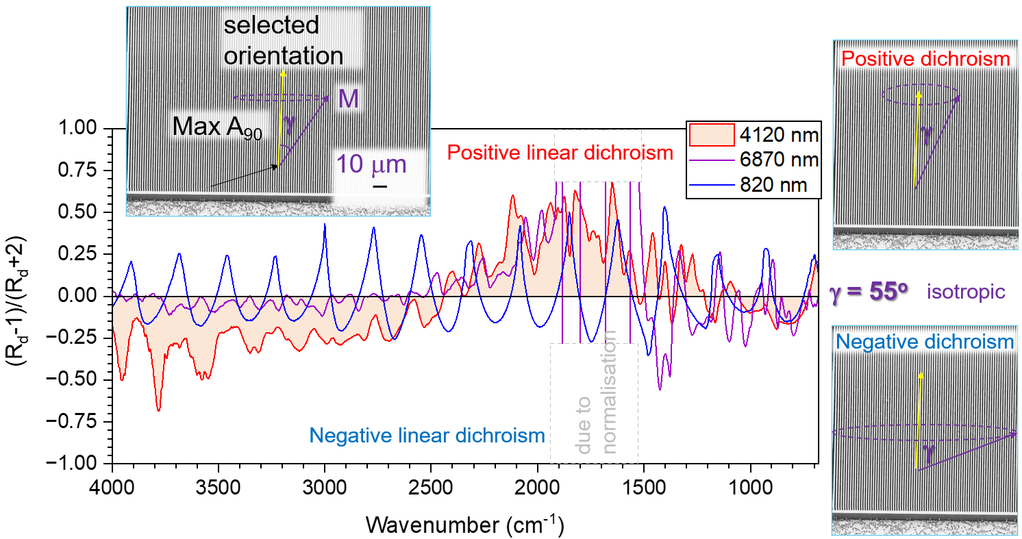
When period of the grating is comparable with the IR wavelength of incident light , the structure imposed changes of reflectance and transmittance are modulated/altered. The intrinsic absorption of diamond stretch over 2600-1700 cm-1 band (3.85-5.88 m). First, a Fourier filter was applied for experimentally measured absorbance spectrum (Fig. 3). The very same filter was applied for all absorbance spectra. Only five gratings with the most strong absorbance at IR (the largest periods) were analysed (see Fig. 2). Figure 4(a) shows filtered absorbance spectra of five gratings at four polarization azimuths. At some spectral region, absorbance at was larger than at as well as the opposite tendency was present. The dichroic ratio is called positive when and negative when (see Sec. IV). From the 4-pol. fits, the amplitude and orientation azimuth were calculated (Fig. 4(b)). The shows jumps of phase by at the locations of the sign change of the dichroism. For example, the iso-polarisation point where absorbance for all four polarisations is the same was at 3000 cm-1 for the m period grating (Fig. 4). This corresponds to the wavelength of m, which is inside diamond with the refractive index of . The isotropic absorbance for the linear polarised incident light would correspond to the quarter-wavelength conditions induced between o- and e-beams due to the form-birefringence in the grating of thickness m, i.e. . One would find , which match the expected value for the grating with duty cycle (the largest birefringence). The phase conditions for a quarter wavelength are repeated over the wavelength (or in phase): where is an integer . For and wavelength m, it is m (or 4003 cm-1) where spectral iso-crossing is expected (Fig. 4). This analysis is applied to a spectral range out of the intrinsic diamond absorbance 2600-1800 cm-1 band; at the absorbance resonance the phase of an oscillator undergoes a change.


As measured spectra of absorbance and reflectance without fringe removal are shown in Supplement. Figure A1 shows and spectra from the very same area of m2 at four polarizations. The reduced absorbance was observed at for 6.87 m (Fig. A1) and 4.12 m (Fig. A2) conditions. In the case of those two periods, the intrinsic diamond band is not discernible due to reduced absorbance (reduced can also be affected by diffraction losses). By color-tracing of the spectra measured at different azimuth of incident polarization, a clear inversion of phase (an intensity reversal between and spectra) was observed in Fig. A2(a) at the intrinsic diamond absorption region. For the smaller period grating of 0.82 m, the spectra are governed by interference and clear free spectral range cm-1 is observed (Fig. A3). The effective refractive index can be determined for the known thickness : cm-1; for m, .

Interestingly, was observed when reflectance was normalised to that of gold mirror (on the sample stage of Bruker microscope). This can be caused by interference and sub-wavelength nature of the structure allowing for constructive field addition in intensity calculation . Strong interference is present in spectra due to the Fabry-Pérot slab multi-reflections. This hampers visualisation of dichroic ratio the dichroic ratio change from positive to negative, however, we used experimentally measured data without Fourier filtering to trace intricate changes of absorption and reflection (see Sec. IV for discussion of ). With Fourier filtering, the sign change of dichroic ratio was present at the same spectral regions, however, there were oscillatory artifacts (not shown here for brevity).
The absorbance can be estimated from the differential reflectance of the diamond grating vs. diamond membrane as , [30] where is the refractive index of diamond. This method is used to calculate absorption of a thin micro-film on a thicker substrate, e.g., resist on a cover glass. Figure A5 shows such presentation for the diamond grating sample. It represents the grating-only contribution to the absorbance. The interference fringes is the main feature, however, there is a clear orientation change between the positive and negative linear dichroism at the diamond absorption region .

III.2 Thin m diamond membranes
Example of laser ablation approach to define opto-mechanical structure with central 0.3-mm diameter disk suspended on two 1-mm-long arms of 10 m width defined in 1-m-thick membrane of diamond is shown in Fig. 5. Semi-circular m wide incisions close to the membrane’s attachment to Si substrate were made by fs-laser 230 fs/1030 nm ablation. The released internal stress formed a cylindrical arc of m height over mm cross-section. The curvature of the cylindrical arc is mm-1 (see bottom inset in Fig. 5).
The protocol of laser cutting by ablation was developed on a diamond membrane without stress release by incisions. To define 1-mm-long bridge, one window was cut out by scanning at single fs-pulse fluence above the graphitisation threshold of 0.3 J/cm2 and below the ablation threshold of 3 J/cm2 [1] (see, Fig. 6). The scanning speed, laser repetition rate and pulse energies were chosen to have at least two-three repeated cycles for a cut (Fig. 6). Once the first window was out, the second window is started with a shift determining the final beam width. Laser scan was started along the beam and progressed to the outside direction from the bridge. In this way, any membrane’s movements due to stress release were minimised, which decreased the likelihood of unexpected lateral repositioning of the bridge in respect to the laser path, which would result in damaging the bridge/beam. The narrowest bridge of 10 m was reliably fabricated. This protocol was used for the longer beam with a disc in the middle (Fig. 5). Carbonisation of the bridge and regions near the cut was apparent from color change. Internal stress of the diamond film was evident when 1-mm-long beam was separated at the one end from the rest of membrane. It moved m from the plane of original membrane (Fig. 6). The final structures with longer span (Fig. 5), were made using more tight focusing with lens at higher fluence J/cm2 in order to have more narrow width of graphitisation affected rim.
The method of progressing from diamond graphitisation to oxidation (burning) is a debris-free method of 3D structuring and laser machining [39]. The energy deposition (dose) should be optimised for controlled removal of diamond into . The presented cutting of long micro-bridges was adopted to reduction of the width of the bridge by side-edge burning with precise control of lateral beam scanning. In this way, the most of the laser focal region is not irradiating the bridge/beam itself. This avoids direct linear momentum deposition (a push by photon pressure), which can break the beam. The Rayleigh length at the used focusing conditions m and allows to side-burn/polish micro-beams (waist/radius was m). With the used objective lens and m focal spot, reliable 1-mm-long beams were made down to 8-10 m. The major limitation is defined by the grain structure of CVD diamond membrane where sub-micrometer sized grains are not uniformly carbonized and burned (see Fig. A6). The grain structure of CVD diamond is also apparent in dry plasma etched regions near gratings (Fig. 1). To remove graphitised carbon from edges of the laser cut of diamond membrane, plasma can be used, which is more selective to rather bonding [42]. The lower oxidation threshold of graphite vs. diamond in [25] could be utilised to reduce amount of graphitisation after laser cut. In fs-laser ablation of bulk high-pressure high-temperature (HPHT) diamonds at comparable high pulse fluence at 800 nm wavelength, graphitisation was found negligible [41]. The regions in fs-laser inscribed modifications inside diamond are located along nano-cracks [3].
IV Discussion
IV.1 An apparent anisotropy of (hence ) due to form-birefringence
One clear evidence from 4-pol. spectra is its complex structure, where the dichroic ratio is changing (Figs. A1, A2) at the different parts of IR spectrum; here is absorbance parallel or perpendicular to the selected direction. The dichroic ratio reveals orientation of the absorbing species in IR and widely used in IR chemical finger printing spectral region [6]. The diamond membrane is isotropic and is expected, especially at the regions were there are no specific absorption bands. However, a clear distinction between regions (at incidence azimuth of E-field polarization, is along the diamond ridges/planes of the grating, so, the o-beam or ) as well as are observed at wavenumbers of high and low intrinsic absorbance parts of the spectrum, respectively (Fig. A2(a)). The absorbance dichroism revealed by 4-pol. analysis has origin in material structural organisation (a grating) which is made out of isotropic poly-crystalline absorbers. The form-birefringence, in theory, should not cause absorbance changes since it only affects state of polarization (ellipticity) of the outcoming beam but not energy losses/absorption. The light scattering, on the other hand, could contribute to the losses and affect the spectral lineshape of the absorbance bands [10].
One possible contribution to enhanced absorbance in a grating structure is due to light intensity redistribution at the interface diamond-air between the walls. This is governed by the boundary conditions for the normal and tangential components of the displacement and at the interface for a non-conductive medium-1 (diamond) with surface charge density and air (medium-2). A change of dichroism from positive to negative occurs at the two sides in respect to the resonance peak [29]. However, in non-absorbing spectral range the apparent dichroism stems from the form-birefringence.

The dichroic function measured experimentally is linked to the angle between the electric dipole-transition moment and selected direction of -field orientation: ; with the absorbance maximum when and zero when at [6]. The when and there is no anisotropy in absorption. At this condition, or . The is plotted for different period gratings in Fig. A4. For the smallest period of 820 nm, the is oscillating with a structure of . However, a change from to is clearly discernible for the 4.12 m grating between positive and negative dichroism. At the intrinsic absorbance region of diamond , i.e., or (positive linear dichroism). There were no any specific changes near the highly reflective Reststrahlen spectral region at the degenerate TO and LO phonon bands, which for diamond are at cm-1 [35], which is also a characteristic Raman line of diamond [14].
IV.2 Numerical model: optical intensity distribution
In order to model light intensity distribution relevant to a comparatively large grating on a diamond membrane, which has dimensions and structures in size, where is the wavelength, a 10× down-scaling was applied in order to apply FDTD (see Fig. 7(a)). FDTD model for the visible wavelength 500 nm was setup up with periodic boundary conditions in the lateral dimensions and the perfectly matching layer (PML) along light propagation to remove scattering and reflections Fig. 7(b). Figure 7(c) shows cross sectional view of the light intensity enhancement in the form-birefringent structure for top-illumination. The corresponds to the normal component and is shown separately from the overall intensity. The back-illuminated intensity cross-section is presented in Fig. 7(d) and the local near-field distribution is apparently different. As required by boundary conditions, the component has largest enhancement at the interface diamond-air at the side-walls of the grating structure. Also, there is enhancement of intensity at the exit interface for propagation from diamond-to-air when there is no phase change for the reflected light. This illustrates the difference of volume where high intensity is localised, hence, were a strong absorption for the and -modes could be expected. The form-birefringent structure is responsible for this energy redistribution and influence transmission (hence absorption) due to different proportions of energy distributed between the diamond and air. The modeling of plane wave irradiation and periodic boundary conditions present the ideal case when all scattered/diffracted light is accounted for. In real experiments, the illumination/collection of the objective lens plays a role since only light within a cone will be measured/collected; here is the refractive index of air (for dry objective lens).
V Conclusions
The and spectral of diamond micro-gratings at IR spectral range showed polarization sensitivity at the intrinsic absorption band of diamond where change of dichroic ratio was changing sign (positive linear dichroism was at the intrinsic absorption region). In a 4-pol. measurement, this corresponded to a reversal between the high and low absorbance. Absorbance was also accessed from the reflectance spectra, and confirmed dichroism reversal. This can be useful for structures when transmittance is not possible to measure directly, which is very common case in complex and integrated micro-structures.
For laser cutting of micrometers-thick diamond membranes, the approach of graphitisation (0.3 J/cm2 threshold) and oxidation is adopted to reduce threshold of ablation (3 J/cm2) and was applied for fabrication of micro-bridges of 1 mm long, m-wide in m-thick diamond membrane. Stress release cuts were essential to define such micro-bridges.
Acknowledgements.
S.J. acknowledges support via ARC DP240103231 grant and Nanophorb (2018-2022) - Nanofabrication technologies towards advanced control of the photon angular momentum - from the National Center for Scientific Research (Le Centre National de la Recherche Scientifique), France. Design of micro-bridges for opto-mechanical applications was provided by Etienne Brasselet. H-H.H. and S.J. are grateful for a research stay at the Laser Research Center, Vilnius University, in 2025. J.M. acknowledges support via JST CREST (Grant No. JPMJCR19I3) and KAKENHI (No.22H02137). M.R. was supported via KAKENHI (Grant No. 22K14200) and SAKIGAKE (Grant No. JPMJPR250E). Part of the supplementary information was acquired using synchrotron-based FTIR microspectroscopic technique on the Infrared Microspectroscopy (IRM) beamline at the Australian Synchrotron, part of ANSTO.References
- [1] (2021) Femtosecond laser micromachining of diamond: current research status, applications and challenges. 179, pp. 209–226. External Links: ISSN 0008-6223, Document, Link Cited by: §III.2.
- [2] (2013) Laser-induced rotation and cooling of a trapped microgyroscope in vacuum. 4, pp. 2374. Cited by: §I.
- [3] (2016-06) Direct observation of graphenic nanostructures inside femtosecond-laser modified diamond. 102, pp. 383–389. External Links: Document, ISSN 00086223 Cited by: §III.2.
- [4] (2018) Designing high-efficiency thin silicon solar cells using parabolic-pore photonic crystals. 9, pp. 044009. Cited by: §I.
- [5] (2020) Photonic crystal light trapping: beyond 30% conversion efficiency for silicon photovoltaics. 5 (2), pp. 020902. Cited by: §I.
- [6] (2022) Infrared linear dichroism for the analysis of molecular orientation in polymers and in polymer composites. 14 (6). External Links: Link, ISSN 2073-4360, Document Cited by: §IV.1, §IV.1.
- [7] (2009) Light-induced nonlinear rotations of nematic liquid crystal droplets trapped in laser tweezers. 512 (1), pp. 143–151. External Links: Document, Link, https://doi.org/10.1080/15421400903050780 Cited by: §I.
- [8] (2026) Bruker, FTIR application notes. Note: Last accessed 26 January 2026; External Links: Document Cited by: Figure A1.
- [9] (2010-06) Colloquium: gripped by light: optical binding. 82, pp. 1767–1791. External Links: Document, Link Cited by: §I.
- [10] (2006) Differential reflectance spectroscopy in analysis of surfaces. In Encyclopedia of Analytical Chemistry, pp. . External Links: ISBN 9780470027318, Document, Link, https://onlinelibrary.wiley.com/doi/pdf/10.1002/9780470027318.a2504 Cited by: §IV.1.
- [11] (2000) Reversible phase transitions in polymer gels induced by radiation forces. 408, pp. 178–181. Cited by: §I.
- [12] (1999-06) Fast optical switching by a laser-manipulated microdroplet of liquid crystal. 74 (24), pp. 3627–3629. External Links: ISSN 0003-6951, Document, Link Cited by: §I.
- [13] (2017, https://api.semanticscholar.org/CorpusID:165157566) The Kramers-Kronig relations : validation via calculation technique. External Links: Link Cited by: Appendix A2.
- [14] (1945) Raman spectrum of diamond. 155, pp. 171. Cited by: §IV.1.
- [15] (2016) Achieving an accurate surface profile of a photonic crystal for near-unity solar absorption in a super thin-film architecture. 10 (6), pp. 6116–6124. Cited by: §I.
- [16] (2026) Bulk hexagonal diamond. 651 (), pp. 621–625. Cited by: §I.
- [17] (2022) Beyond lambertian light trapping for large-area silicon solar cells: fabrication methods. 5 (9), pp. 210086. Cited by: §I.
- [18] (1999) Photophysics and photochemistry of a laser manipulated microparticle. 24 (5), pp. 665–697. External Links: ISSN 0079-6700, Document, Link Cited by: §I.
- [19] (2005) Control of the molecular alignment inside liquid-crystal droplets by use of laser tweezers. 1 (6), pp. 656–661. External Links: Document, Link, https://onlinelibrary.wiley.com/doi/pdf/10.1002/smll.200500038 Cited by: §I.
- [20] (2008) Two-photon excitation of dye-doped liquid crystal by a cw-laser irradiation. 489 (1), pp. 310 – 319. External Links: Document, Link, https://doi.org/10.1080/15421400802218785 Cited by: §I.
- [21] (2007-10) Laser trapping of deformable objects. 15 (20), pp. 13310–13317. External Links: Link, Document Cited by: Appendix A3.
- [22] (2005) All-optical control of microfluidic components using form birefringence. 4, pp. 530–533. Cited by: §I.
- [23] (2012-01) Kramers–Kronig Analysis Of Infrared Reflectance Spectra With A Single Resonance. 1, pp. 67 – 76. External Links: ISSN 2180-3722, 0127-9696, Document Cited by: Appendix A2.
- [24] (2012-05) A simple method for the kramers-kronig analysis of reflectance spectra measured with diamond anvil cell. 359 (1), pp. 012013. External Links: Document, Link Cited by: Appendix A2, Appendix A2.
- [25] (2012) Hyperthermal oxidation of graphite and diamond. 45 (11), pp. 1973–1981. Note: PMID: 22694904 External Links: Document, Link, https://doi.org/10.1021/ar200317y Cited by: §III.2.
- [26] (2026) Sharp diamond needles for single-photon emission. 7 (2), pp. e202500302. External Links: Document, Link, https://advanced.onlinelibrary.wiley.com/doi/pdf/10.1002/adpr.202500302 Cited by: Appendix A3.
- [27] (2025) Integration of laser-patterned photonic crystals in si solar cells. 13 (35), pp. e01781. Cited by: §I.
- [28] (2021-04) Hard x-ray transient grating spectroscopy on bismuth germanate. 15 (7), pp. 499–503. External Links: ISSN 1749-4893, Link, Document Cited by: §II.1, §III.1.
- [29] (2021) Hyperspectral molecular orientation mapping in metamaterials. 11 (4). External Links: Link, ISSN 2076-3417, Document Cited by: §IV.1.
- [30] (2016) Light-induced reflectivity transients in black-si nanoneedles. 144, pp. 221–227. External Links: ISSN 0927-0248, Document, Link Cited by: §III.1.
- [31] (2025) Self-organized nanostructures formed by femtosecond laser processing of graphite electrode: nanogratings, nanoparticles, and nanofilaments. 192, pp. 113873. Cited by: Appendix A3.
- [32] (2026) Shimadzu application notes. Note: Last accessed 31 January 2026; External Links: Document Cited by: Appendix A2.
- [33] (1963) Elementary Theory of the Optical Properties of Solids. In Solid State Physics, F. Seitz and D. Turnbull (Eds.), Vol. 15, pp. 299–408. External Links: ISSN 0081-1947, Document, Link Cited by: Appendix A2.
- [34] (2024) Optical tweezers assembled nanodiamond quantum sensors. 24 (39), pp. 12188–12195. Note: PMID: 39291712 External Links: Document, Link, https://doi.org/10.1021/acs.nanolett.4c03195 Cited by: §I.
- [35] (2005) FTIR spectra of faceted diamonds and diamond simulants. 14 (10), pp. 1592–1599. External Links: ISSN 0925-9635, Document, Link Cited by: §IV.1.
- [36] (2014) Optofluidic sorting of material chirality by chiral light. 5, pp. 3577. Cited by: §I.
- [37] Towards 30. Cited by: §I.
- [38] (2024) Femtosecond laser direct writing of flexible electronic devices: a mini review. 17 (3). External Links: Link, ISSN 1996-1944, Document Cited by: §I.
- [39] (2023-03) Fresnel zone plate sculptured out of diamond by femtosecond laser for harsh environments. 48 (6), pp. 1379–1382. External Links: Link, Document Cited by: §III.2.
- [40] (2025) Synthesis of bulk hexagonal diamond. 644 (), pp. 370–375. Cited by: §I.
- [41] (2010-06) On femtosecond micromachining of hpht single-crystal diamond with direct laser writing using tight focusing. 18 (12), pp. 13122–13135. External Links: Link, Document Cited by: §III.2.
- [42] (2023) The etching mechanisms of diamond, graphite, and amorphous carbon by hydrogen plasma: a reactive molecular dynamics study. 6 (11), pp. 2300371. External Links: Document, Link, https://advanced.onlinelibrary.wiley.com/doi/pdf/10.1002/adts.202300371 Cited by: §III.2.
- [43] (2010) Designable 3d nanofabrication by femtosecond laser direct writing. 5 (5), pp. 435–448. External Links: ISSN 1748-0132, Document, Link Cited by: §I.
Appendix A1 Anisotropy in and -modes: no fringe removal
Figure A3 presents -spectra for 820 nm period grating (0.5 duty cycle). This is sub-wavelength structure showing strong oscillatory signals due to thickness of entire structure on the membrane being only 4-10 times larger than the wavelength of the light source.
Figure A4 shows spectra of dichroic function with change of linear dichroism at the intrinsic absorption window of diamond.
Figure A5 presents absorbance spectra calculated from the differential reflectance , which represents absorbance only in the grating structure since for the reference a thinned diamond membrane region was used (reflectance ).
Appendix A2 Kramers-Kronig determination of refractive index from reflectance spectra
Assessing absorbance from reflectance can also be achieved by Kramers-Kronig analysis. The complex amplitude of the reflected light wave is a function of the phase difference between the incident and reflected waves , where is the phase angle. The reflectance . The refractive index is given by [24]:
| (A1) |
For experimentally measured spectra , the phase is obtained for each frequency value from the Kramers-Kronig relation [24]:
| (A2) |
This integral has poles at and can be calculated using the double Fourier transform method [32]:
| (A3) |
where is the cyclic frequency. By measuring wide IR spectrum range benefits recovery of and allow to estimate absorbance or optical density (from reflectance only) , where is the thickness and the absorption coefficient [cm-1].
Appendix A3 Graphitisation of diamond
Figure A6 shows close up optical images of bridges fs-laser cut out from diamond membrane shown in Fig. 6. Cross polarized imaging showed that there was no stress induced at the vicinity of anchoring sites of the beam/bridge. Whiskers of micrometer size were recognisable along the laser oxidised tracks and could be due to the diamond orientation controlled propensity to oxidation [26]. Degree of graphitization can be determined using Raman and IR spectroscopes which are sensitive to changes in and bonding and corresponding C-C vibration bands [31].
At more tight focusing (Fig. A7) the final cut out of a suspended disk on two side beams of 1 mm length was made. Attempt was made to thin the width of 10 m beam/bridge by extra passes of the laser beam at higher pulse energy (power). At higher laser power and tighter focusing, the lateral force can push out high refractive index material (diamond ) as well as pull into laser beam depending of the actual position of object and focal spot [21].