Geant4 Optical Simulation without C++
Abstract
The plain text geometry description syntax in Geant4 has been extended to incorporate optical properties for bulk materials and surface interfaces. This extension enables users to configure and execute comprehensive optical simulations without writing C++ code, significantly lowering the learning curve and eliminating the need for frequent recompilation. In this paper, we detail the implementation of the new :prop and :surf tags and validate them through examples of key optical processes, including Cherenkov radiation, scintillation, Rayleigh scattering, and absorption. Furthermore, we provide a thorough demonstration of configuring complex optical boundaries using the UNIFIED model. These capabilities are contextualized through practical scenarios, showcasing the extension’s potential for rapid prototyping and simulation studies.
Program Summary
Program Title: GEARS - Geant4 Example Application with Rich features and Small footprint
Developer’s repository link: https://github.com/jintonic/gears
Licensing provisions: MIT
Programming language: C++
External routines/libraries: Geant4, CMake
Nature of problem: Configuring Geant4 optical simulations traditionally requires advanced C++ programming, creating a steep learning curve and necessitating time-consuming recompilation during the iterative detector design process.
Solution method: We extended the Geant4 plain text geometry syntax with custom tags for defining bulk and surface optical properties. These text-based definitions are parsed at runtime, enabling fast, C++-free configuration of complex optical simulations.
keywords:
Geant4 , Monte Carlo Simulation , Optical Simulationorganization=Department of Physics, University of South Dakota,addressline=414 E. Clark St., city=Vermillion, postcode=57069, state=SD, country=USA
1 Introduction
Geant4 [1, 2, 3] is a widely used toolkit for simulating the passage of particles through matter, including optical photons. It provides three methods to define detector geometry and material: C++, GDML [4], and plain text with some simple syntax [7]. All of them are introduced in the Detector Definition and Response section in Geant4 User’s Guide for Application Developers (Geant4 User’s Guide in short hereafter) [9] with an obvious emphasis on C++.
1.1 C++ VS GDML & Plain Text
However, detector definition in C++ requires fair amount of knowledge of C++ programming and the usage of Geant4 classes. This creates a steep learning curve for beginning physicists and engineers. In addition, it requires re-compilation every time a change is made, no matter how small. This is very inconvenient, especially during the iterative design and debugging phase.
In contrast, GDML and plain text geometry definitions do not require compilation at all, allowing for fast and frequent updates to a geometry setup.
1.2 GDML VS Plain Text
GDML is akin to HTML in that it uses a structured and verbose XML-based syntax, which provides greater flexibility and precision but requires familiarity with its syntax rules. Plain text geometry description, on the other hand, is more like Markdown [10]: simple, intuitive, and easier to write and read, making it ideal for quick prototyping and debugging.
In fact, GDML is created as an intermediate format to facilitate the exchange of geometry information between different tools, such as FreeCAD [6], Geant4, and ROOT [13]. It is meant to be generated by one piece of software and read by another. The strict and structured XML-based syntax is well suited for this purpose. However, its complexity can be a barrier for users who want to quickly define and modify geometries without delving into the intricacies of XML syntax. On the other hand, plain text geometry description is designed to be written by human, allowing users to easily create and modify geometries without the need for extensive knowledge of XML or programming.
1.3 Optical Simulation
Optical simulation in Geant4 typically requires C++ coding to define optical properties of a bulk material and/or an interface (surface) between two materials [9]. However, it suffers the same drawbacks described previously. Optical properties can also be defined using GDML with, however, some limitation, for example, optical properties cannot be assigned to existing NIST materials pre-defined in Geant4 [5], such as G4_AIR, etc.
Although the standard plain text geometry definition in Geant4 lacks syntax for optical properties, we have extended it to include them for both bulk materials and surfaces. This allows users to perform optical simulations without C++ coding, making the process more accessible and user-friendly.
1.4 Article Structure
In this article, we first introduce our extension to the plain text geometry definition syntax for defining optical properties in Section 2, and then demonstrate its usage and accuracy in simulating optical properties of bulk materials (Section 3) and optical interfaces (Section 4), individually. The demonstration is done primarily through the application of this extension to scintillation crystals wrapped with various reflectors and read out by common photo-sensors, such as photomultiplier tubes (PMTs) or silicon photomultipliers (SiPMs). Finally, we summarize the work and discuss its implications in the concluding section.
2 Plain Text Extension
The plain text geometry definition in Geant4 utilizes tags (keywords with a proceding colon) to define various aspects of the geometry, such as :solid for a 3D shape, :mate for a material, and :volu for a Geant4 logical volume. For example,
defines a logical volume named CsI as a tube with an inner radius of 0, an outer radius of 3 cm, a half-length of 5 cm, and made of the built-in NIST material G4_CESIUM_IODIDE.
We have added two new tags to define optical properties for bulk materials (:prop) and surfaces (:surf), following the instruction in section Defining new tags in the geometry file format in the plain text geometry definition manual [7]. The C++ code is included in a single-file Geant4 application, GEARS - Geant4 Example Application with Rich features and Small foodprint [11], that can parse the extended plain text geometry description in an ASCII file (detector.tg, for example), and set up the optical simulation accordingly. A new Geant4 macro command, /geometry/source, is also introduced in GEARS to specify the geometry definition file:
2.1 New Tag :prop
The :property (or :prop in short) tag is introduced to define both constant and energy dependent optical properties of a bulk material:
For example:
Note that the material specified in the :prop tag must be defined previously using the :mate tag or be a built-in NIST material in Geant4, such as G4_CESIUM_IODIDE.
Both tags and properties are case-insensitive. Properties that contains more than one word, such as ScintillationYield, can be written in camel case [14] to increase readability.
A list of optical properties and their meanings can be found in section Optical Photon Processes in Geant4 User’s Guide [9].
2.2 New Tag :surf
The :surface (or :surf in short) tag is introduced to define optical properties for a surface (interface between two physical volumes):
where [vol.1]:[#] means the name of physical volume 1 and its copy number # [9]. Copy number is necessary to uniquely identify a specific placement of a volume that may be placed multiple times. For example:
Note that properties specified in the :surf tag are assigned to the interface between two physical volumes identified by their names and copy numbers, and they must be defined at the end of the :surf code block after the property keyword.
2.3 Usage
To use the extension, a user needs to provide at least two text files to GEARS: 1. a detector definition file, for example, detector.tg, with optical properties defined using the new tags, and 2. a macro file, for example run.mac, generating optical photons in the detector system.
Listing 3 shows a minimal working example of run.mac. It instructs Geant4 to simulate 1000 times a 3.5 eV optical photons emitted isotropically from the center of a detector defined in detector.tg.
It is possible to pull optical property definitions out of detector.tg and place them in a separate file, for example, CsI77K.tg, as shown in Listing 1, which can be included back in detector.tg as shown in Listing 4.
The advantage of this approach is that the optical property definition file CsI77K.tg can be reused in various detector definition files.
When parsing the optical definition code, GEARS will print out the following messages on screen for the user to verify whether the definitions are correctly recognized.
In the following sections, we demonstrate the application of the extended plain text geometry definition through various example snippets of geometry definition files, macro files, and simulation results.
3 Material Optical Properties
The effectiveness of configuring optical properties of a bulk material using the :prop tag is verified through a few key optical properties defined in the Optical Photon Processes section [9] in Geant4 User’s Guide. Some of them are for the generation of optical photons, such as scintillation and Cherenkov radiation, while others are for the transportation of optical photons, such as absorption length and Rayleigh scattering length.
3.1 Cherenkov Radiation
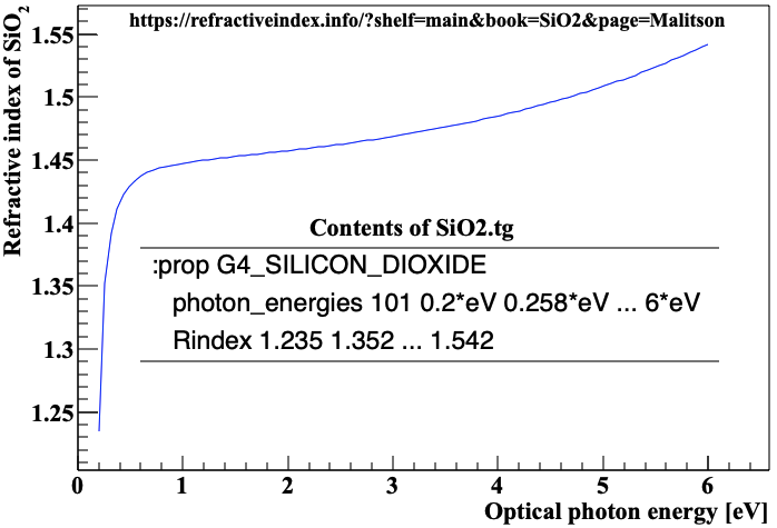
Cherenkov radiation is emitted when a charged particle travels through a dielectric medium at a speed greater than the phase velocity of light in that medium. The refractive index of the medium is a key parameter that determines the Cherenkov threshold and the angle of emission [8]. In general, the refractive index is energy dependent, and it is defined using the Rindex property in the :prop tag. Figure 1 shows the refractive index of silicon dioxide (SiO2) taken from Ref. [12]. Saved in file SiO2.tg are 101 data points along this curve as shown in the code snippet in Figure 1. This file can then be included in a detector definition file, for example, PMTwindow.tg, to define the refractive index of SiO2, a common material used in PMT windows, as shown in Listing 5.
PMTwindow.tg can then be used by a Geant4 macro file, for example, cherenkov.mac, to simulate Cherenkov radiation emitted by a 511 keV electron passing through a PMT window, as shown in Listing 6.
The simulation can be performed by executing command gears cherenkov.mac in a terminal. Figure 2 shows the visualization of Cherenkov photons (green) emitted along an electron trajectory (red) in a PMT window (blue). The detailed step-by-step tracking information can be printed out on screen for verification using Geant4 macro command /tracking/verbose 2, as shown in Listing 7.

Note that optical photons are generated as secondary particles through an electron multiple scattering (msc) process instead of an explicit Cherenkov process. To verify that they are really Cherenkov photons, one can disable the Cherenkov radiation process by uncommenting line 3 in Listing 6, and re-run the simulation. The output tracking information, as shown in Listing 8, confirms that no optical photons can be generated during the electron multiple scattering process if the Cherenkov process is disabled.

Figure 3 shows the energy spectrum of Cherenkov photons generated in the PMT window. The artificial cut-off of the spetrum at 6 eV is due to the lack of refractive index data above 6 eV in SiO2.tg. The rest of the spectrum follows roughly the refractive index curve shown in Figure 1. This is because the energy of a photon is sampled from the density function below [8]:
| (1) |
where is the photon energy, is the refractive index of the medium at energy , and is the velocity of the charged particle relative to the speed of light in vacuum. The smaller the refractive index, the smaller the density function, and thus fewer photons are generated at that energy.
3.2 Scintillation
Geant4 provides many properties to fine-tune the emission of scintillation photons in a bulk material, such as light yield, resolution scale, time constants, and emission spectra, etc. [9]. As an example, Listing 1 shows the definition of those properties for a pure CsI crystal at liquid nitrogen temperature (77 K), and Listing 4 shows how this file is used in a detector definition file, detector.tg. Listing 9 shows snippet of Geant4 macro file scintillate.mac used to simulate the emission of scintillation photons generated at the center of the crystal after it absorbs a 1 keV ray.
The simulation can be performed by executing command gears scintillate.mac in a terminal. Figure 4 shows the visualization of scintillation photons (green) emitted from the center of a cylindrical CsI crystal (blue circle) after it absorbs a 1 keV ray, the trajectory of which is too short to be seen. Photon tracks end at the boundary of the crystal because no refractive index is defined beyond the crystal in this simulation. Since Geant4 cannot predict the behavior of optical photons without knowing the refractive index beyond the boundary, it kills the photons upon their arrival at the boundary. Viewing along the axial direction of the cylindrical crystral, some photon tracks appear to be shorter than others because they are killed at the front and back surfaces of the crystal instead of being absorbed in the crystal.

Figure 5 shows numbers of scintillation photons emitted in 5,000 simulated events. It peaks around 101, matching the expected value of 1 keV 100/keV within the statistic uncertainty. Assuming Poisson statistics, the width of this distribution should be around . The sigma of the red Gaussian fit is about 4.4 times larger, matching the setting of ResolutionScale within the statistic uncertainty.

Figure 6 and 7 show the emission time distributions of scintillation photons in large and small ranges, respectively. The two exponential decay components are clearly seen, their values obtained from exponential fittings (colored curves) match the time constants defined in Listing 1 within statistic uncertainties. Note that the slow time constent is fixed to 1000 ns in the fitting of the fast component to improve the fitting stability.


Figure 8 shows the energy spectrum of scintillation photons emitted in the CsI crystal. Two Gaussian functions (blue and magenta) are used to fit the distribution simultaniously. Their means and sigmas match the 3.67 and 4.3 eV emission spectra defined in CsI77K.tg (Listing 1 shows only a snippet of the entire file). The mornalization factors, norm1 and norm2, represent the total areas instead of the heights of the Gaussian distributions. Their ratio is , much larger than the ratio given by ScintillationYield2/1 (0.98/0.02=49). This is likely due to a bug in Geant4’s implementation of ScintillationYield1,2, etc. Further investigation is needed to confirm this. But practically, one can always adjust ScintillationYield1,2 to achieve the desired ratio of the two emission components.

3.3 Rayleigh Scattering
Optical photons can be scattered by small particles in a medium through Rayleigh or Mie scattering depending on the size of particles [9]. In a typical scintillation crystal, such as CsI, the size of atoms is in the order of a few tenth of nm, much smaller than the typical optical photon wavelength, which is in the order of a few hundred nm. The dominant scattering mechanism hence is Rayleigh scattering.
The Rayleigh scattering length is defined through the property Rayleigh in Geant4, as shown in Listing 1. To verify the effectiveness of this configuration, 3.5 eV optical photons (green trajectories) are shot along the z axis of a long cylindrical CsI crysatl as shown in the Geant4 visualization imbedded in Figure 9. The distance between the origin and the first scattering point of each trajectory is accumulated in the histogram shown in Figure 9. It is niced described by an exponetial decay function (red) and the decay constant cm given by the fitting matches the set value of 339 cm within statistic uncertainties.

3.4 Absorption Length
In addition to be scattered, optical photons can also be absorbed by a medium. The absorption length is defined through the property AbsLength in Geant4, as shown in Listing 1. Again, to verify the effectiveness of this configuration, 3.5 eV optical photons are shot along the z axis of a long rectangular CsI crystal as shown in the Geant4 visualization imbedded in Figure 10. The distance between the origin and the absorption point of each trajectory is accumulated in the histogram shown in Figure 10. It is nicely described by an exponetial function (red) and the constant cm given by the fitting matches the set value of 30 cm within statistic uncertainties.

Note that scattering parameters are disabled in this simulation to avoid interference, and vice versa in the previous Rayleigh scattering simulation.
4 Surface Optical Properties
When an optical photon generated in a dielectric material travels to the boundary of that material, it reaches an optical interface (or optical surface using Geant4 terminology) between two materials, the one that it is about to leave and the one that it is about to enter. Optical properties of the material where the photon is generated cannot determine the fate of the photon on its own. As a minimal requirement, optical properties of the material that the photon is about to enter also need to be specified. More generally, certain properties of the interface itself may need to be specified as well, such as its roughness, etc., and they are independent from optical properties of the two materials on the two sides of the interface. The :surf tag is dedicated to the configuration of these surface optical properties. If the :surf tag is not specified, the program defaults to the ideal surface mentioned in the next section.
4.1 Ideal Surface
An ideal interface is the simplest case of an optical interface. In this case, no additional property of the interface itself is needed. The fate of an optical photon reaching the interface is determined solely by the refractive indexes of the two materials on the two sides of the interface, and , following Snell’s law and Fresnel equations [9].
Figure 11 visualizes the behavior of optical photons (green) on an ideal optical interface between CsI and a PMT window made of SiO2. Photons are shot from the CsI crystal (blue) towards the PMT window (black) at different incident angles. As expected, at a smaller incident angle, some photons are refracted into the PMT window while others are reflected back into the CsI crystal, at a larger angle, all photons are totally reflected, following Snell’s law and Fresnel equations.

This simulation is done by placing a CsI crystal defined in Listing 4 and a PMT window defined in Listing 5 next to each other in a detector definition file. The refractive indices of the two materials are provided in the included files CsI77K.tg (Listing 1) and SiO2.tg (Figure 1), respectively. No more optical property is needed to define the interface between the two materials. A Geant4 macro file similar to Listing 3 is used to shoot 3.5 eV optical photons from the CsI crystal towards the PMT window at different incident angles.
4.2 The UNIFIED Model
Defining optical properties of a surface goes beyond the ideal interface described above. Geant4 provides several models to define more complex optical surfaces, among which the UNIFIED model is the most versatile one [9]. Listing 2 shows an example of defining an optical surface using the UNIFIED model in the extended plain text geometry syntax. In the following sections, we first demonstrate the implementation of the UNIFIED model using the extended syntax for the dielectric_dielectric interface with various surface finishes. The dielectric_metal interface will be discussed after that.
4.3 Unpainted Dielectric Surfaces
While Geant4 does not explicitly use the term unpainted as a reserved keyword, it is used here to categorize surfaces where the optical boundary is defined solely by the interface between two dielectric media. Two finishes are available for these surfaces in the UNIFIED model: and , each introduces more optical parameters for increased flexibility.
4.3.1 Polished Finish
The polished finish in the UNIFIED model can be regarded as an extension of the ideal interface discussed in Section 4.1. It allows users to specify two new parameters: Reflectivity (R) and Transmittance (T). Both parameters must be within the range , and their sum must satisfy . If , Geant4 will redefine as and as such that the sum of the newly defined and is equal to 1.
It is crucial to note that these parameters are settings, not physically calculated probabilities derived from Snell’s law or Fresnel equations.
Specifically, Transmittance (T) defines the ratio of incident photons that immediately pass through the surface without further optical processing. Photons transmitted in this manner retain the polarization state of the incident photon. Setting may seem artificial, but it is particularly useful for modeling complex physical components as simplified geometric planes. A primary example is the metal wire mesh commonly found in time projection chambers. Rather than simulating each individual wire, a user can define a flat plane with equal to the open-area ratio of the mesh, allowing transmitted photons to continue their tracks in the subsequent volume. Another typical use case is a partial polarizer, where a specific fraction of light is intended to pass through the boundary while strictly preserving its original polarization state.
Conversely, Reflectivity (R) specifies the ratio of photons reserved for processing by physics laws; they will be subjected to the standard Geant4 reflection/refraction calculations based on the refractive indices and the angle of incidence.
A third parameter, Absorption (A), is not specified by the user but is instead calculated from the user-defined settings via the simple energy conservation relation:
This parameter represents the ratio of incident photons that are absorbed at the surface.
The ideal interface described in Section 4.1 represents a specific configuration of the polished finish where (and consequently ). Since these values constitute the model’s default settings, a surface declared as polished without explicitly defined or values will behave identically to an ideal interface.
In a more general configuration, where , , and such that , the fate of an incident photon is determined by a pseudo-random number generator, as illustrated conceptually in Figure 12. When a photon reaches the surface, a uniformly distributed random number is generated within the range . The result is determined by comparing against the defined parameters:
-
1.
If , the photon’s outcome is calculated based on the standard optical physics rules, including Snell’s Law and Fresnel equations.
-
2.
If , the photon is directly transmitted through the interface.
-
3.
If , the photon is absorbed at the surface.

It is worth noting that the parameter names are somewhat misleading due to the probabilistic nature of the first case. Even when a random number falls into the Reflectivity range (Case 1), the subsequent physics-based calculation may still result in the photon being refracted through the interface, provided it is allowed by the refractive indices and the angle of incidence. Thus, Reflectivity () does not represent the probability of reflection, but rather the probability of applying a physics-based calculation. Similarly, Transmittance () is not the probability of transmission calculated from physics, but an artificial setting that controls the probability of a photon passing through the interface without any change in direction or polarization.
Listing 10 demonstrates the implementation of this finish in GEARS using the extended text geometry syntax. Here, a polished interface named CsI2Epoxy is defined between a CsI crystal (copy number 1) and an optical epoxy layer (copy number 2).
Figure 13 demonstrates the result with this setting. Because the sum of probabilities is unity (), no photons are absorbed. The large is not set based on reality, but to exaggerate its effect. Half of the photons undergo transmission, passing straight through the interface without any change in direction. The other half undergo a standard physical calculation, resulting in either reflection or refraction.

This distinction between the transmitted and refracted photons is clearly visible in the figure: the transmitted ones continue along their original trajectory, whereas the refracted ones bend further at an angle relative to the surface normal, consistent with the change in refractive index between the two media.
Figure 14 demonstrates another configuration featuring a polished interface with and . In this scenario, half of the incident photons are absorbed at the boundary, while the other half undergo a calculation via physics laws. To illustrate this, photons are directed onto the interface at an oblique angle. Approximately half of the tracks terminate at the interface, verifying the setting. The remaining photons either refract into the epoxy or reflect specularly, consistent with physics laws.

4.3.2 Ground Finish
The ground finish within the UNIFIED model is designed to simulate a rough interface between two dielectric materials. The roughness is modeled by treating the interface as a collection of microscopic facets, or micro-facets in short, randomly oriented around the average surface normal, as shown in Figure 15.
The azimuthal angle of the micro-facet normal with respect to the average surface normal is uniformly sampled within , which cannot be seen in the 2D schematic. The polar angle between the micro-facet normal and the average surface normal is sampled from a Gaussian distribution with mean 0 and standard deviation , as shown in Figure 16. If is larger than , an incident photon from the upper dielectric material will hit the back side of a micro-facet, which is physically impossible.
Apparently, the larger is, the rougher the surface is. Empirically, lapped or machine-polished surfaces generally correspond to radian, while satin or fine-ground finishes typically fall within the 0.09–0.21 radian range. Coarser surfaces, such as those that are milled or sandblasted, may require values exceeding 0.26 radian. When is too large, say, 1.0 radian, the chance for a randomly sampled to be larger than becomes significant, a few new samplings will be done until a valid is obtained. This is highly inefficient and should be avoided. A new parameter, sigma_alpha, is introduced to specify , and its upper bound is set to the smaller of and to ensure sampling efficiency.
On highly rough surfaces, an optical photon may undergo multiple reflections across several micro-facets. In such cases, Geant4 determines the refraction angle, and the reflection and refraction probabilities based on the first micro-facet orientation. However, the final reflection angle falls into four different scenarios as shown in Figure 17. The probability of each scenario is determined by three additional parameters introduced below.
- Back scattering
-
happens when a photon undergoes multiple reflections within deep grooves on the surface and eventually scatters back toward its starting point. The probability of this scenario, , can be specified by parameter backscatterConstant.
- Specular spike
-
represents specular reflection about the average surface normal. Its probability can be specified by parameter specularSpikeConstant.
- Specular lobe
-
represents a reflection about the micro-facet normal rather than the average surface normal. The probability of this scenario, , can be specified by parameter specularLobeConstant.
- Diffuse lobe
-
represents Lambertian reflection. The probability of this scenario is . No new parameter is needed to specify this scenario.
The usage of these new parameters is demonstrated in Listing 11, which shows the application of this finish to a nonpolished CsI crystal wrapped with Teflon.
Figure 18 shows the case where and other constants are zero. Within CsI, photons undergo backscattering reflection about the average surface normal. The directions of refracted photons in Teflon are randomized due to the small variation of the micro-facet orientation ( radians).

Figure 19 shows the case where and other constants are zero. Within CsI, photons undergo specular spike reflection about the average surface normal. The refracted photons in Teflon are diffused a bit due to the small variation of the micro-facet orientation ( radians).

Figure 20 shows the case where and other constants are zero. Within CsI, photons undergo fuzzy specular reflection about the average surface normal. The directions of both reflected and refracted photons are randomized due to the small variation of the micro-facet orientation ( radians).

If none of the constants is specified, they are initialized to zero. The finish defaults to pure Lambertian reflection because .
Figure 21 is generated using settings in Listing 11 without line 6, 7, 8, 9. Photons undergo Lambertian reflection in CsI. Photons refracted in Teflon are diffused a bit due to the small variation of the micro-facet orientation ( radians).

It is worth noting that the ground finish serves as a functional superset of the polished finish and the ideal interface. As shown in Figure 22, by setting and , the standard polished logic is exactly replicated. Under these constraints, if we further require , all incident photons will propergate according to physics laws, and the ideal optical interface logic is recovered.
4.4 Painted Dielectric Surfaces
For surfaces painted or wrapped with reflective layers, the nomenclature in the UNIFIED model shifts: while polished and ground previously referred to the nature of the dielectric interface itself, here they characterize the paint. Explicitly, the descriptor ground indicates that the paint functions as a diffusive (Lambertian) reflector, whereas polished identifies the paint as a specular (mirror-like) reflector. The prefixes, front and back, distinguish the interaction sequence: front implies immediate photon-paint interaction (Figure 23), whereas back implies the photon first traverses the gap before encountering the paint (Figure 24).
We will start with the discussion of the ...frontpainted finishes and then proceed to the ...backpainted ones.
4.4.1 PolishedFrontPainted Finish
The polishedfrontpainted finish defines a surface coated with a specularly reflective paint.
The functional distinction between this and the polished finish lies in the interpretation of the reflectivity parameter, . For a polished interface, dictates the probability that a photon undergoes an optical physics calculation to determine whether it reflects or refracts. Conversely, for a polishedfrontpainted finish, physics laws are bypassed. directly specifies the probability that a photon undergoes purely specular reflection. No refraction is possible for the polishedfrontpainted finish as shown in Figure 25. Parameter and the calculated absorptivity behave the same in both finishes.
A real-life application of this finish is the simulation of a first-surface (or front-surface) mirror (FSM), such as those used in telescopes or laser optics. Unlike a standard household mirror (second-surface mirror) where light passes through glass before reflecting, a FSM has the reflective coating on the front side of the substrate. A photon traveling in air strikes the coating immediately and undergoes specular reflection off the coating, without reaching the substrate beneath it at all. As a result, the optical properties of the substrate beneath the coating do not matter and hence do not need to be specified.
However, if a non-zero is given, that portion of photons will enter the subtrate as if the coating were not there. Users need to specify the optical properties of the substrate if they want to track these artificially transmitted photons. Listing 12 gives an example of a FSM with 95% reflectivity and 5% transmittance. Its results are shown in Figure 26.

4.4.2 GroundFrontPainted Finish
This finish models a surface coated with a diffusive reflective layer. A canonical application is the integrating sphere, designed to homogenize incident light using multiple diffusive reflections. These devices typically consist of a hollow cavity, coated in its inner surface with a highly diffusive material such as white BaSO4 powder or sintered PTFE (Teflon). In the context of luminous flux metrology, a light source is suspended centrally within the cavity to measure its total optical power. By capturing the full spherical emission ( steradians) and scattering it repeatedly against the cavity walls, this geometry spatially averages the light field, effectively eliminating errors that would otherwise arise from the source’s specific angular directionality.
Listing 13 defines the optical surface for half of such a sphere, where the inner wall is treated as a 99% reflective diffuse coating. Only 1% of photons are absorbed on the coating. The output of the simulation is shown in Figure 27.

4.4.3 Back Painted Finishes
Back painted finishes can be understood as the combination of a ground finish between dielectric 1 and the gap (dielectric 2) with a front-painted surface, as shown in the relation schematic in Figure 28. Whether it is polished or ground is determined by the front painted finish, not the finish of the interface between dielectric 1 and the gap, which is always ground:
It should be explicitly noted, however, that attempting this conceptual recreation requires the manual definition of three separate physical volumes: dielectric 1, the gap, and the external wrapper. The explicit backpainted finishes, therefore, provide a streamlined mechanism to simulate this complex three-tier volume interaction efficiently without requiring the manual definition of a microscopic gap volume. The refractive index of the gap must be explicitly defined as a parameter of the surface as shown in Listing 14. Otherwise, the photon will be killed upon encountering the surface.
4.5 Summary of Dielectric-Dielectric Surfaces
Table 1 summarizes parameters that determine the optical behavior of different types of dielectric-dielectric surfaces. It is worth emphasizing that, while is defined for the interface, and are properties of the bulk materials instead of the interface; they need to be defined so that photons can be properly propagated in those materials. From this point of view, a surface with a front painted finish requires zero parameter to function.
| Surface and | Required | Optional |
|---|---|---|
| Finish Types | Parameters | Parameters |
| ideal | - | |
| polished | ||
| ground | ||
| polishedFrontPainted | ||
| groundFrontPainted | ||
| polishedBackPainted | ||
| groundBackPainted |
Default values of the optional parameters are , which results in the default behaviors listed in Table 2.
| Finish Types | Default Behavior |
|---|---|
| polished | ideal reflection and refraction |
| ground | Lambertian reflection, ideal refraction |
| polishedFrontPainted | specular reflection only |
| groundFrontPainted | Lambertian reflection only |
| polishedBackPainted | Lambertian and specular reflection |
| groundBackPainted | Lambertian reflection only |
4.6 Dielectric-Metal Surfaces
The interaction of electromagnetic waves with metallic surfaces is fundamentally different from dielectric-dielectric interfaces due to the high density of free electrons in conductors. When a photon strikes a metal, the oscillating electric field induces a rapid motion of these electrons, which in turn radiates an electromagnetic field that effectively cancels the incident field within the material. Consequently, electromagnetic waves cannot penetrate deep into the metal; instead, they are confined to a very thin skin depth, typically on the order of a few nanometers for visible and ultraviolet light. The macroscopic result of this interaction is high reflectivity.
For most metals used in detector construction, the reflectivity remains high until the photon energy approaches the material’s plasma frequency (). At this threshold, the electrons can no longer respond fast enough to cancel the field, and the metal begins to behave more like a transparent dielectric. The energy corresponding to the plasma frequency () typically falls in the vacuum ultraviolet (VUV) range for common metals. For example, aluminum has a high plasma energy of approximately eV ( nm), making it an excellent reflector for most optical applications. Other common metals like silver and gold have plasma energies around 9.0 eV and 9.1 eV respectively, while copper sits at approximately 10.8 eV. Since the energy of scintillation photons is typically in the range of 2–5 eV, bulk metals can be regarded as opaque to them. For this reason, T can be kept at its default value of 0, while R can be set slightly lower than 1 to account for some surface absorption due to the energy loss to heat through ohmic dissipation. Cherenkov photons, on the other hand, may have energyies approaching or exceeding the plasma frequencies of the metal they interact with. T can be adjusted according to experimental data to account for the increased transparency.
In addition to specifying the R and T parameters, Geant4 allows one to specify a complex refractive index, , where the imaginary part (), also known as the extinction coefficient, dictates the rate of absorption within the skin depth. Parameters corresponding to these two indices are called realRindex and imaginaryRindex. It is important to note that these parameters are generally applicable for photon energies below the plasma frequency; above this threshold, the index of refraction for metals is no longer accurately described by the simple free electron model, requiring more complex treatment or empirical data.
4.6.1 Polished
The polished dielectric_metal surface essentially exhibits the same behavior as the polishedFrontPainted dielectric_dielectric surface. Its reflectivity and absorption rate can be fine-tuned by adjusting the R and T parameters guided by the general discussion provided previously.
4.6.2 Ground
The ground dielectric_metal surface behaves much like the groundFrontPainted dielectric_dielectric surface, in that the photon interacts immediately with the surface upon confronting it and there is no refraction. It differs notably in that if there is a reflection, the reflection type can be affected by the three user defined constants: , , and , as discussed in the ground finish section for dielectric_dielectric interfaces.
4.7 Look-Up Tables
An alternative to the parameter-driven UNIFIED model is the Look-Up Table (LUT) approach. While the UNIFIED model relies on the manual specification of multiple optical properties, such as , , , and , etc. LUT models, on the other hand, utilize pre-calculated or measured datasets to determine the fate of an incident photon. In these models, the complex interactions at the boundary are encapsulated within the table itself.
The primary advantage of the LUT approach is its ease of configuration. From a user’s perspective, the setup is significantly more straightforward because it requires no manual parameter tuning. One simply selects a predefined finish, such as polishedVM2000Glue or groundTyvekAir, as shown in listing 15, and the simulation automatically handles the optical response. This turnkey functionality eliminates the need for the iterative optimization often required to find the correct or reflection coefficients for a specific physical surface, making it particularly useful for simulating standard detector materials that are well-characterized and consistent across different experimental setups.
Despite their convenience, LUT models are fundamentally limited in scope compared to the UNIFIED model. Because they rely on specific experimental datasets, they are only available for a select range of surface finishes and material interfaces. Consequently, the LUT approach is not a universal solution; if a user is simulating a custom material, a unique surface treatment, or a boundary condition not covered by the existing libraries, they must revert to the UNIFIED model’s parameter-based framework to manually construct the surface’s optical profile.
5 Conclusion
In this work, we introduced an extension to the Geant4 plain text geometry syntax that allows for the comprehensive definition of optical properties without C++ programming. Through the newly developed :prop and :surf tags, users can seamlessly assign both constant and energy-dependent optical properties to bulk materials and intricate surface boundaries.
We validated this implementation against a broad spectrum of optical phenomena, successfully reproducing the expected physical behaviors for Cherenkov radiation, scintillation, Rayleigh scattering, and optical absorption. Additionally, we demonstrated the extension’s robust capability to handle diverse surface configurations by extensively exploring the UNIFIED model, covering polished, ground, and painted finishes for both dielectric-dielectric and dielectric-metal interfaces.
By interpreting text-based optical property definitions at runtime, this approach bypasses the time-consuming C++ compilation cycle and makes Geant4 optical simulations significantly more accessible. The modular nature of the text files encourages the reuse of optical property definitions across different detector geometries. Ultimately, this development streamlines the iterative design of complex optical systems, facilitating rapid prototyping and advanced simulation efforts for future applications like the operation of pure CsI detectors at cryogenic temperatures in dark matter and neutrino experiments.
6 Acknowledgements
This work is supported by the NSF award OIA-2437416, PHY-2411825, and the Office of Research at the University of South Dakota. Computations supporting this project were performed on High Performance Computing systems at the University of South Dakota, funded by NSF award OAC-1626516.
7 Declaration of Use of AI Tools
During the preparation of this work, the authors used Gemini to generate the initial draft of this manuscript. After using this tool, the authors reviewed and edited the content as needed and take full responsibility for the content of the published article.
References
- [1] (2003) Geant4: a simulation toolkit. Nucl. Instrum. Meth. A 506, pp. 250–303. External Links: Document Cited by: §1.
- [2] (2006) Geant4 developments and applications. IEEE Trans. Nucl. Sci. 53 (1), pp. 270–278. External Links: ISSN 1558-1578, Document Cited by: §1.
- [3] (2016) Recent developments in Geant4. Nucl. Instrum. Meth. A 835, pp. 186–225. External Links: ISSN 0168-9002, Document Cited by: §1.
- [4] (2006) Geometry Description Markup Language for Physics Simulation and Analysis Applications. IEEE Trans. Nucl. Sci. 53 (5), pp. 2892–2896. External Links: ISSN 0018-9499, Document Cited by: §1.
- [5] (2019) Adding optical properties to built-in Geant4 materials using GDML. Note: https://geant4-forum.web.cern.ch/t/340/4 Cited by: §1.3.
- [6] (2025) FreeCAD. Note: https://www.freecad.org/ Cited by: §1.2.
- [7] (2025) Geant4 Geometry from Text File Version 1.0. Note: https://geant4.web.cern.ch/collaboration/workingi_groups/persistency/docs/textgeom.pdf Cited by: §1, §2.
- [8] (2025) Geant4 Physics Reference Manual. Note: https://geant4-userdoc.web.cern.ch/UsersGuides/PhysicsReferenceManual/html Cited by: §3.1, §3.1.
- [9] (2025) Geant4 User’s Guide for Application Developers. Note: https://geant4-userdoc.web.cern.ch/UsersGuides/ForApplicationDeveloper/html Cited by: §1.3, §1, §2.1, §2.2, §3.2, §3.3, §3, §4.1, §4.2.
- [10] (2004) Markdown. Note: https://daringfireball.net/projects/markdown Cited by: §1.2.
- [11] (2025) GEARS - Geant4 Example Application with Rich feature and Small foodprint. Note: https://github.com/jintonic/gears Cited by: §2.
- [12] (2025) Refractive index database. Note: https://refractiveindex.info Cited by: §3.1.
- [13] (2025) ROOT Data Analysis Framework. Note: https://root.cern/ External Links: Document Cited by: §1.2.
- [14] (2025) Camel case. Note: https://en.wikipedia.org/wiki/Camel_case Cited by: §2.1.