Development of Nb-GaAs based superconductor semiconductor hybrid platform by combining in-situ dc magnetron sputtering and molecular beam epitaxy
Abstract
We present Nb thin films deposited in-situ on GaAs by combining molecular beam epitaxy and magnetron sputtering within an ultra-high vacuum cluster. Nb films deposited at varying power, and a reference film from a commercial system, are compared. The results show clear variation between the in-situ and ex-situ deposition which we relate to differences in magnetron sputtering conditions and chamber geometry. The Nb films have critical temperatures of around and critical perpendicular magnetic fields of up to at . From STEM images of the GaAs-Nb interface we find the formation of an amorphous interlayer between the GaAs and the Nb for both the ex-situ and in-situ deposited material.
Keywords:
niobium, dc magnetron sputtering, semiconductor superconductor hybrid materials, in-situ superconductor growthI Introduction
Superconductor (SC) semiconductor (SE) hybrid (SSH) devices have re-emerged Takayanagi and Kawakami 1985; Bending et al. 1990; Nguyen et al. 1992 fueled by the hope of finding anyons in solid state systems and their subsequent application for fault tolerant quantum computing Kitaev 2003; Nayak et al. 2008; Alicea et al. 2011; Karzig et al. 2017; Aguado 2020. Most notably the search for the Majorana Fermion in solid state systems has attracted attention Das et al. 2012; Mourik et al. 2012. This promoted numerous experiments in Andreev interaction with Quantum Hall states Wan et al. 2015; Lee et al. 2017; Gül et al. 2022 and topological superconductivity Sato and Ando 2017; Fornieri et al. 2019.
The achievement of epitaxial growth of thin film Al on III-V SEs Pilkington and Missous 1999; Krogstrup et al. 2015 sparked experiments in SSH devices Chang et al. 2015; Kjaergaard et al. 2016; Shabani et al. 2016; Drachmann et al. 2017; Kjaergaard et al. 2017; Suominen et al. 2017; Casparis et al. 2018; Bøttcher et al. 2018; O’Farrell et al. 2018; Lee et al. 2019; Mayer et al. 2019; Drachmann et al. 2021; Nichele et al. 2020; Whiticar et al. 2020; Haxell et al. 2022a; Haxell et al. 2022b; Banerjee et al. 2022. The crucial element of material synthesis is the in-situ deposition, enabling an undisturbed SC-SE combination, crucial for a transparent interface to electron transport Krogstrup et al. 2015. The formation of sub-gap states and a electrostatic barrier, degrading the performance of the hybrid system, is associated to the surface oxide, formed when the SC is deposited ex-situ Chang et al. 2015.
Therefore, nanowires and two dimensional electron systems (2DES) based on InAs and InSb with an epitaxial Al layer have become the established material platform exhibiting a pronounced proximity effect Krogstrup et al. 2015; Chang et al. 2015; Güsken et al. 2017. Furthermore, Al is typically available in molecular beam epitaxy (MBE) systems owing to its use in III-V semiconductor growth.
The superconducting properties of epitaxial Al films limit the temperature and magnetic field range of Al-based SSH experiments to of around at film thicknesses between and Kjaergaard et al. 2016; Shabani et al. 2016; Bøttcher et al. 2018; Lee et al. 2019; Mayer et al. 2019. The reported perpendicular critical fields range from Drachmann et al. 2017 up to Mayer et al. 2019 at dilution fridge temperatures.
The search for an alternative to Al is the subject of a multitude of recent studies Güsken et al. 2017; Carrad et al. 2020; Kanne et al. 2021; Pendharkar et al. 2021; Dang et al. 2021; Perla et al. 2021; Kousar et al. 2022. A wide range of elemental superconductors has been deposited onto nanowires including Pb Khan et al. 2020; Kanne et al. 2021, In Bjergfelt et al. 2021, Ta Carrad et al. 2020, V Bjergfelt et al. 2019 and Sn Pendharkar et al. 2021; Khan et al. 2020. Nb is of particular interest Güsken et al. 2017; Perla et al. 2021; Carrad et al. 2020 as it has the highest bulk critical temperature and magnetic field of all the elemental SCs Buzea and Robbie 2005. Pb appears to be the best alternative so far Khan et al. 2020; Kanne et al. 2021 owing to its favourable lattice match to InAs Jelver et al. 2017 and relatively high Tc Kanne et al. 2021.
Exciting research proposals van Heck et al. 2012; O’Brien et al. 2018; Fatemi et al. 2021 call for building increasingly complex SSH devices and networks. In this application lithographically patterned 2DES-SC SSH represent a promising approach Lutchyn et al. 2018. The 2DES in InAs Haxell et al. 2022a and InSb Lei et al. 2022a can be grown to reasonably high mobilities but lack far behind 2DES based on GaAs Külah et al. 2021. The drawback of GaAs is the Schottky barrier McLean 1988 which is expected to suppress the proximity effect Blonder et al. 1982. Nonetheless induced superconducting gaps in bulk n-GaAs employing in-situ deposited Al have been measured Taboryski et al. 1996; Kutchinsky et al. 1997. In this context our recently developed shallow GaAs 2DESs Külah et al. 2021 are posing an interesting unexplored potential for SSHs.
The interaction between the SE and SC is not limited to the proximity effect. A type-II superconductor can shape the magnetic field in the SE underneath via its vortices Weeks et al. 2007 forming the basis of exciting experimental proposals Rosenberg et al. 2009; Zocher and Rosenow 2016; Okugawa et al. 2022. Vortex interaction mediated experiments have been previously attempted Bending et al. 1990; Kruithof et al. 1991 most notably by Geim et al. Geim et al. 1992a; Geim et al. 1992b. The authors investigated Pb on a GaAs 2DES and concluded that a SC with a small vortex is needed together with a low electron density 2DES as close as possible to the surface Geim et al. 1992c. These requirements are rooted in a geometrical argument, considering the size of the magnetic field variation at the depth of the 2DES versus the size of the quasiparticle in the 2DES as a function of magnetic field. The small vortex size Ghenim et al. 2004 can be achieved in Nb and the lowest electron densities have been reached in (Al)GaAs based systems 2DES Sajoto et al. 1990.
In this work, we present the first results from our chamber for DC magnetron sputtering of SC on our MBE grown III-V SEs without breaking the vacuum. In the initial experiment, we compare Nb deposited in-situ at varying power in the UHV dc magnetron sputtering system and ex-situ deposited in a commercial system (AJA Int.). The samples are of high purity but display significant differences in surface roughness and crystallite orientation which can be related to the growth regime.
We compare the superconducting properties of the Nb film, by investigating the resistive transition as a function of temperature and magnetic field. STEM images of the Nb-GaAs interface reveal an amorphous interlayer at the interface for both the in-situ and ex-situ depositions.
II MBE and Magnetron Sputtering Cluster
The layout of the UHV cluster, consisting of two molecular beam epitaxy (MBE) machines and the SC deposition system, is presented in fig.1 a). The first MBE chamber is optimized for high mobility 2DES in (Al)GaAs Berl et al. 2016; Meyer et al. 2019; Röösli et al. 2020; Scharnetzky et al. 2021; Külah et al. 2021 while the other covers a wider range of III-V materials based on As and Sb Lei et al. 2019; Karalic et al. 2019; Shibata et al. 2019; Shibata et al. 2020; Lei et al. 2020; Lei et al. 2022a; Lei et al. 2022b. The UHV magnetron sputtering chamber is connected via a UHV tunnel to enable in-situ deposition of SCs on MBE grown SEs as well as preventing contamination of the MBE systems.

The incorporation of oxygen in superconducting films is generally believed to have a detrimental effect on the superconducting properties such as the critical temperature Koch et al. 1974. Therefore, the system was designed to minimize contaminants, specifically the incorporation of oxygen. The UHV magnetron sputtering chamber is supplied with purified gas and solely pumped by a cryo pump in order to obtain elementally clean films, see supplementary for details Todt et al. 2023. After bakeout the system achieved the mass spectra presented at the bottom fig.1 b). The black line represents the pumped state at while the red line at was taken 18hrs after the deposition of Nb. The pressure is dominated by peaks from the different ionization states of Ar and its isotopes (36, 38). A peak associated with water three orders of magnitude smaller than Argon can be identified after deposition indicated by the arrow. Continued use of the chamber reduced the water peak below detection limit and therefore we assume that it originated from residual water in the gas lines.
The kinetic rather than thermal nature of magnetron sputtering offers an alternative path to the evaporation for SC deposition on SEs. The film growth via evaporation is primarily controlled by substrate temperature and rate Palmstrom 1995. In order to produce connected films of low melting point elements such as In, Pb or even Al on SE surfaces, the substrate has to be typically cooled below room temperature Sands et al. 1990; Brillson 2010; Kanne et al. 2021; Krogstrup et al. 2015 adding technical complexity. SC with higher melting points such as Ta and Nb can be grown at higher substrate temperatures Perla et al. 2021. However, to evaporate these low vapor pressure metals Alcock et al. 1984 they have to be heated to high temperatures causing the chamber to release contamination from the chamber walls and heat up the substrate surface. Magnetron sputtering, on the other hand, is a comparatively cold deposition method Mattox 2010.
The method appeals additionally with the possibility to grow nitrides, a simple material exchange, wide variety of compounds from mixed targets and co-sputtering as well as a moderate pressure during deposition which limits outgassing Mattox 2010. This opens up the possibility to deposit a wide range of compound materials such as A15 and B1 phase SCs as well as more exotic variants like MgB2 Mičunek et al. 2006.
II.1 Sample preparation
Both the ex-situ and in-situ Nb films were deposited onto of MBE grown n++ GaAs. The ex-situ wafer was removed from the MBE chamber after growth. Before loading it into the AJA magnetron sputtering system the wafer was etched in a 1:1 solution of HCl ():H2O at temperature until the surface was hydrophilic to remove the oxide. The wafer was then transferred in air to the load lock within 5 min. The in-situ wafer was moved in our UHV tunnel from the MBE chamber to the UHV magnetron sputtering chamber under a residual pressure of .
II.2 Nb depositions
In order to investigate the possible operating conditions in our sputtering system, a characterisation of the Nb sputtering rate for various power and pressure combinations was made. This exploration served as a starting point to determine which sputtering conditions could be compared to the commercial AJA system and could yield films with good superconducting parameters.
The dependence of the Nb deposition rate on pressure and set power for our system was investigated using a quartz crystal balance that can be moved into the wafer position and results are presented in fig.2. The rate increases with pressure up to at which point the Nb growth is limited by diffusion from the Ar gas. With increasing pressure the voltage decreases and the current increases as expected from a denser and more conductive plasma. The rate is linearly dependent on the set power at a given pressure.
The deposition in our system with inch UHV magnetrons from Angstrom Sciences is controlled by pressure, power and substrate heating. The parameters used in this study are summarised in table 1. The guns are mounted such that we can vary the substrate target distance under a fixed angle of and the substrate is not rotated. For this study we chose to fix the distance at the minimum of . The commercial system employs a inch target away from the substrate in a planar orientation and a constant substrate rotation. The pressure was chosen such that the pressure-distance product is for both setups.
Due to the difference in target size between the systems it is not possible to attain the same rate at the same current and voltage values for both setups. The ex-situ system can attain a low voltage of at a high rate while the in-situ machine is limited to before the plasma becomes unstable at .

| sample | substrate | p | Tsub | voltage | J | rate | Rsq |
| () | () | () | () | () | () | ||
| ex-situ | GaAs | 10 | RT | 214 | 24.2 | 5.0 | 0.95 |
| in-situ - A | GaAs | 9 | RT | 404 | 3.7 | 0.6 | 1.84 |
| in-situ - B | GaAs | 9 | RT | 582 | 10.6 | 2.7 | 1.75 |
| in-situ - C | GaAs | 9 | RT | 708 | 17.4 | 5.0 | 2.03 |
| Dobrovolskiy and Huth 2012 B2 | Al2O3 | 4 | 850 | 312 | 2.5 | 5.0 | 0.7 |
| Imamura et al. 1992 | Si | 23 | RT | 270 | 74 | 27.3 |
III Structural and Elemental Analysis
III.1 AFM

Fig.3 shows the surface morphologies of the Nb films measured by AFM. All samples have randomly distributed elongated grains, roughly long and wide. The elongated grains are not oriented with respect to the substrate or the source. Since randomly oriented elongated Niobium grains are also observed on a silicon substrate by Imamura et. al. Imamura et al. 1992, a direct relationship between this effect and the GaAs substrate seems unlikely.
The root mean square roughness values obtained from the AFM data using Gwyddion Nečas and Klapetek 2012 are listed in the last column of table 1. The in-situ films are distinctively rougher than the ex-situ film with little difference between the in-situ films.
III.2 XRD
XRD measurements were performed with a PANalytical X’PERT PRO MPD diffractometer in Bragg-Brentano reflection geometry and Cu K radiation. The measurements of the Nb films are plotted in fig.4. The data was acquired under a offset of the sample tilt relative to the symmetric geometry to minimize the signal from the GaAs substrate. The signal from the (001) oriented GaAs substrate still appears as broad background centered at , which is coming from thermal diffuse scattering. Apart from the substrate signals, no significant differences are observed between the measurements with and without offset.
Comparison of our XRD data with literature de Freitas et al. 2016; Wilde et al. 2018 shows that our in-situ Nb films are missing the reflections associated with the (211) orientation parallel to the substrate surface de Freitas et al. 2016; Wilde et al. 2018. The ex-situ film, on the other hand, only shows the 110 and 220 reflections indicating that the crystallites, making up the uniform film, have a preferential orientation of the (100) planes with respect to the substrate.
The relative peak heights of the 110 family of reflections and the 200 reflection vary between the in-situ samples while the 310 signal appears unchanged. Depending on deposition voltage the orientation distribution either the (110) or (200) oriented crystallites appears to vary. However, it is not a direct trend as the largest variation is observed for the in-situ - B sample.
III.3 Elemental analysis
Rutherford Back Scattering (RBS) measurement of the Nb films were undertaken. The RBS was performed using Helium ions under a back-scattering angle of . The particle induced X-ray emission (PIXE) from the sample was measured in parallel. No significant contamination of the Nb film could be conclusively detected within the capabilities of RBS and PIXE, see supplementary for details Todt et al. 2023.
III.4 Discussion
The possible origin of the observed structural variations between the in-situ and ex-situ films could be related to different deposition parameters, namely voltage, substrate surface and or geometric differences between the two sputtering systems.
It appears, that the large kinetic energy difference related to different powers used for the in-situ samples do not make a significant difference in their structure that could be identified with the implemented characterization methods. A step up in deposition voltage between the in-situ and ex-situ samples does exist. However, we observed very little structural change when changing the voltage from 404V to 708V for samples in-situ - A,B and C. Given that both systems work at the same pressure distance product, this does not point to the deposition voltage as the root cause for our observed structural differences.
To aid in understanding our findings and bring our deposition conditions into context with those from published literature which have been appended to table 1.
Dobrovolskiy et al. Dobrovolskiy and Huth 2012 have reached the Stranski-Krastanov regime growth regime Mattox 2010 and produced epitaxial Nb films at on Al2O3. The key differences between the reference film by Doborvolskiy et al. and our material is the Al2O3 substrate which not only has a favourable lattice match but also allows for the required high substrate temperature. The high quality clean limit film listed in table 1 has been grown at the same rate as our ex-situ and in-situ - C samples. In terms of voltage current conditions the reference film is comparable to our in-situ - A sample which suggests that the authors had a smaller substrate target distance to achieve a ten fold higher rate at roughly half the pressure. The roughness increased with elevated growth rate corresponding to a larger voltage which could either be due to the kinetic energy of arriving species or adatoms that didn’t have enough time to reach a kink site.
Imamura et al.Imamura et al. 1992 report similarly elongated grains on their Nb films deposited on Si at room temperature. The distance pressure product employed by Imamura et al. is close to ours at which could explain the close resemblance. The authors find that with reducing pressure or equivalently increasing voltage the width of the XRD peaks reduces (therefore crystallite size increases) and the surface becomes smoother. Specifically, the strain went from tensile to compressive at which corresponds to the point at which crystallite size and roughness did not change anymore. Our in-situ samples deposited at voltages appeared to follow this in that roughness and crystallite size did not change.
The random crystallite orientation seen in the XRD in fig.4 on the in-situ material suggests that the Nb does not find a preferential orientation with the substrate. The in-situ material presents the clean GaAs surface reconstruction while the ex-situ material was exposed to air. It is therefore less likely that the XRD findings are not originating from the Nb-GaAs interface.
The film growth as we understand it has been discussed in detail by Monti et al. Monti et al. 2023. Randomly nucleated crystallites grow in the direction of the facet that incorporates new material at the highest rate. Which facets grow is determined by the surface energy of the specific facet, the adatom mobility on the surface, the direction and rate of the arriving Nb. This will result in the crystallites with favourable orientation to outgrow and terminate neighbouring crystallites until only dendrites of one orientation remain.
The fact that the ex-situ sample only shows the (110) family of crystal orientations parallel to the substrate surface, could therefore originate from a fast saturation of the termination process. The (110) facets thus grow the fastest and terminate their neighbours faster in the ex-situ system than in the in-situ system. The in-situ samples on other hand have not reached the point at which slower growing crystallites are buried resulting in a rougher surface and more crystallite orientations appearing in the XRD. The (211) oriented crystallites have been buried early on in both systems and do not appear at all in the XRD data.
IV Nb superconducting properties
The critical temperature and critical magnetic field of the Nb films limit the measurement range of SSH devices. is the field applied perpendicular to the film at which the resistive transition occurs, termed the upper critical field associated with type-II superconductors Kerchner et al. 1981. Knowledge of the resistive superconducting transition can additionally be used to estimate the coherence length of the Cooper pairs. When compared to the mean free path of the electrons the coherence length determines whether the superconducting film is in the clean or dirty limit Tinkham 1996.
In the context of proximity induced superconductivity the coherence length appears in the pair breaking parameter indicating that a larger coherence length enhances the pair breaking within the superconductor towards the interface Schäpers et al. 2003.
Van der Pauw structures were made and measured using standard lock-in techniques to determine the sheet resistance as a function of temperature and magnetic field , see supplementary for details Todt et al. 2023. The result of measuring the resistive transitions at a constant temperature, while sweeping the magnetic field, is given in fig 5.
The extracted values are significantly higher than expected for clean limit films which have values of or less Peroz and Villard 2005; Dobrovolskiy and Huth 2012. It has been reported that dirty limit films have increased critical fields Dobrovolskiy and Huth 2012; Peroz and Villard 2005 while the critical temperature is lower. The large critical field of our films indicates that these are in the dirty limit with the ex-situ sample being closest to the clean limit. The results shown in fig.5 indicate that, even for room temperature Nb depositions, it is possible to obtain films with less structural defects by changing the sputtering parameters such as power and voltage.
| sample | eq.2 | eq.8 | ||||
|---|---|---|---|---|---|---|
| () | () | () | () | () | () | |
| ex-situ | 9.2 | 47.8 | 0.8 | 1.48 | 15 | 2.3 |
| in-situ - A | 9.0 | 32.7 | 1.1 | 1.59 | 14 | 2.1 |
| in-situ - B | 9.0 | 43.8 | 0.8 | 1.73 | 14 | 1.9 |
| in-situ - C | 8.9 | 71.7 | 0.5 | 1.83 | 13 | 1.8 |
| Dobrovolskiy and Huth 2012 B2 | 9.1 | 0.45 | 83 | 0.7 | 22 |
The target film thickness was chosen to be such that the superconducting critical temperature Zaytseva et al. 2014 and critical field Quateman 1986 of Nb are not expected to significantly change with variations in thickness Minhaj et al. 1994; Zaytseva et al. 2020. The thicknesses are determined from QCM deposition rates and time with the in-situ - B sample being slightly thinner at .
IV.1 Mean free path
Estimating from the Drude formula Ashcroft and Mermin 1976
| (1) |
requires knowledge of the normal state resistivity , the carrier density and the effective mass at a temperature just above the superconducting transition. Ideally, each of these parameters is determined from a separate measurement. However, it is common Gubin et al. 2005; Hazra et al. 2009; Dobrovolskiy and Huth 2012 for Nb films to estimate just from using the expression by Mayadas et al. Mayadas et al. 1972, given as
| (2) |
The normal state resistivity of the sample is calculated from the measured resistance at and zero applied magnetic field using Schroder 2006
| (3) |
where is the Nb film thickness determined from the QCM rate and deposition time. The extracted values do compare well with published values Gubin et al. 2005; Leo et al. 2011; Dobrovolskiy and Huth 2012; Pinto et al. 2018; Zaytseva et al. 2020 and are listed in fourth column of table 2.
IV.2 Ginzburg Landau coherence length
The Ginzburg- Landau (GL) coherence length , which denotes the characteristic length scale over which the order parameter varies, is arrived at via the upper critical field
| (4) |
where is the magnetic flux quantum in type-II superconductors.
To obtain a value for the zero temperature critical field has to be estimated. The resistive transition from fig.5 is not linear down to zero temperature and cannot be simply extrapolated. Werthamer, Helfand and Hohenberg (WHH) Werthamer et al. 1966 arrived at a relevant theory taking into account non-magnetic impurities, spin paramagnetism and spin-orbit scattering at high fields based on initial results by Maki Maki 1966. The relevant result from WHH has been presented by Gurevich et al. Gurevich 2003 as
| (5) |
Applying this theory produces the values for and presented in table 2. The GL coherence length compares well with previously reported values Dobrovolskiy and Huth 2012; Ilin et al. 2014; Wang et al. 1999 and the expected are one order of magnitude larger than what has been achieved with thin Al films Mayer et al. 2019.
IV.3 Bardeen Cooper Schrieffer coherence length
Although eq.2 is an established method, there are critiques relevant in the context of thin polycrystalline films Fuchs 1938; Mayadas and Shatzkes 1970; Vancea et al. 1987. It therefore is warranted to sanity check the consistency of eq.2 with the Ginzburg-Landau-Abrikosov-Gor’kov (GLAG) theory Mangin and Kahn 2016. It connects the findings of GL and Bardeen-Copper-Schrieffer(BCS) for dirty limit films giving a relation between and Tinkham 1996 near as
| (6) |
where is the BCS coherence length at zero temperature.
The BCS theory defines the as the average distance between the two electrons making up a Cooper pair determined by the uncertainty principle Mangin and Kahn 2016. It reads
| (7) |
where is the zero temperature BCS gap and the Fermi velocity. Mayadas et al.Mayadas et al. 1972 arrive at in their derivation of eq.2. Using this value we obtain between for the ex-situ film and for the in-situ - C film.
| (8) |
which expresses the upper critical field to be a linear function of temperature near .
IV.4 Discussion
Despite the observed structural changes, the critical temperatures of our Nb films vary only by a few . The of the epitaxial clean limit film from Dobrovolskiy et al. listed for comparison in table 1 falls within the range of our results.
The resistivities of the in-situ samples increase going down the table correlating with the deposition voltage from table 1. The upper critical field increases significantly going down the table for all samples. Higher resistivities indicate structural degradation which in turn presents more pinning sites for vortices increasing the critical field Welp et al. 2002; Welp et al. 2005. A significant structural change in AFM and XRD data has only been observed between the ex-situ and in-situ samples but not between in-situ samples. Thus the electrical measurements appear to be more sensitive to structural changes than the AFM and XRD analysis.
Although the ex-situ material is smoother and has a preferred crystallite orientation perpendicular to the surface it does not have the lowest resistivity, but a lower critical field and higher critical temperatures. The superconducting properties, AFM and XRD data all indicate a more homogeneous film which should result in a lower resistivity as exemplified by the reference film by Dobrovolskiy et al. listed in table 2. An explanation could be that the ex-situ film is thinner than we expect.
The resistivity of the clean limit reference film from Dobrovolskiy et al. is two orders of magnitude smaller despite the film being half as thick. The additional effect of surface scattering to the resistivities of thin films Fuchs 1938; Mayadas and Shatzkes 1970 does not appear to be significant down to the thickness of the reference film. The large resitivities in our dirty limit films therefore do originate in the structural differences.
The mean free path listed in table 2 compared to the extracted coherence lengths confirms that our films are in the dirty limit. The critical field of the clean limit reference film in table 2 is . Reducing the power and hence the voltage for our in-situ depositions brings us closer to the clean limit. However, at the given pressure distance of , we are limited to the results from in-situ - A as the lowest power that results in a stable plasma.
V Nb-GaAs interface
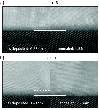
ADF STEM images presented in fig.6 were taken of the Nb-GaAs interface before and after annealing at for which is the annealing recipe for ohmic AuGeNi contacts to n++ GaAs Baca and Ashby 2005. An amorphous interlayer can be seen for both the in-situ - B and ex-situ samples. The thicknesses of the amorphous interlayer indicated in the images were determined by comparing the normalised brightness, see supplementary for details Todt et al. 2023. The ex-situ amorphous interface, initially being thicker than in the in-situ one, is unaffected by the heat, while the in-situ material shows an increased thickness after tempering.
The amorphous interface thickness does not increase when annealed for the ex-situ sample while for the in-situ it does by . The Nb-GaAs interface is expected to be sharp up to for ex-situ deposited films Ding et al. 1988. However, the quality of the TEM images presented by Ding et al. Ding et al. 1988 appear to be the limiting factor in the comparison and the interlayer cannot be resolved. Nb deposition on clean GaAs surfaces via magnetron sputtering has been reported Kutchinsky et al. 1996; Giazotto et al. 2001 but is lacking structural investigation of the interface.
The best reference for in-situ Nb are evaporated films on InAs nanowires, which similarly show an amorphous interlayer Güsken et al. 2017; Perla et al. 2021; Carrad et al. 2020. The origin of the interlayer is attributed to the formation of a NbxAsy compound, which would explain our findings.
VI Conclusion
We have investigated both the structural and superconducting properties of Nb films in-situ deposited on GaAs in a newly designed magnetron sputtering chamber connected to an UHV MBE cluster. An exceptionally high purity of the material was achieved by designing a UHV compatible gas supply system, as proven by the residual gas analysis of the chamber and elemental analysis of the resulting Nb films.
The structural analysis via AFM of the Nb films revealed a marked difference in surface roughness between our in-situ samples and a reference ex-situ sample, deposited in a commercial system. Varying the deposition power for the in-situ samples had little effect on the surface. XRD measurements further support that difference, with the ex-situ sample having only the (110) crystallite orientation with respect to the substrate surface. The in-situ samples all showed (110), (200) and (310) oriented crystallites, despite significant differences in deposition voltages. This difference in crystallinity is attributed to the nucleation and growth of individual crystallites in the polycrystalline film.
Measuring the superconducting resistive transition showed that the films are in the dirty limit with excellent and values. The values did not vary significantly despite at steady increase of with deposition voltage associated with structural degradation. The in-situ method produces pure films underpinned by RBS and PIXE measurements.
The values reflected subtle structural differences between the in-situ films. With increasing deposition voltage the critical field increased, indicating that an increased power does have an effect, although we did not to resolve a trend in film structure by AFM or XRD.
All the investigated Nb - GaAs interfaces exhibited an amorphous interface layer. Tempering the samples to widens the amorphous layer for the in-situ - B but not the ex-situ sample. It is unclear if the formation of the amorphous alloy between the materials is purely chemically driven or if it is related to the sputtering process. Interestingly, its presence in the in-situ deposited samples shows that it is not related to the formation of the native oxide on the semiconductor. Similar phenomena were reported in literature, and the findings indicate that it is related to formation of NbxAsy alloy Güsken et al. 2017; Perla et al. 2021; Carrad et al. 2020.
The presented results validate in-situ magnetron sputtering as a new path to combine Nb and GaAs. Work is ongoing to employ a wider range of III-V semiconductors and superconductors to built a wider material platform for SSH.
VII Acknowledgement
The authors would like to thank Walter Bachmann, Andreas Stuker and by extension the entire workshop of the physics department of the ETH. Without their technical expertise, and more importantly patience, this system would have never been realised. Furthermore, we acknowledge Luca Alt, who built in large parts the setup used to measure the critical field and temperature and Werner Dietsche for an open ear and fruitful discussions. The project was financially supported by the Swiss National Science Foundation (SNSF). We thank the IBM Quantum Academic Network for financial support.
The authors gratefully acknowledge ScopeM for their support and assistance in this work, as well as the support of the clean room operations team of the Binning and Rohrer Nanotechnology Center (BRNC) and the support from Marilyne Sousa (IBM).
References
- Takayanagi and Kawakami (1985) H. Takayanagi and T. Kawakami, Physical Review Letters 54, 2449 (1985), ISSN 0031-9007.
- Bending et al. (1990) S. J. Bending, K. von Klitzing, and K. Ploog, Physical Review B 42, 9859 (1990), ISSN 0163-1829, 1095-3795.
- Nguyen et al. (1992) C. Nguyen, H. Kroemer, and E. L. Hu, Physical Review Letters 69, 2847 (1992), ISSN 0031-9007.
- Kitaev (2003) A.Yu. Kitaev, Annals of Physics 303, 2 (2003), ISSN 00034916.
- Nayak et al. (2008) C. Nayak, S. H. Simon, A. Stern, M. Freedman, and S. Das Sarma, Reviews of Modern Physics 80, 1083 (2008), ISSN 0034-6861, 1539-0756.
- Alicea et al. (2011) J. Alicea, Y. Oreg, G. Refael, F. von Oppen, and M. P. A. Fisher, Nature Physics 7, 412 (2011), ISSN 1745-2473, 1745-2481.
- Karzig et al. (2017) T. Karzig, C. Knapp, R. M. Lutchyn, P. Bonderson, M. B. Hastings, C. Nayak, J. Alicea, K. Flensberg, S. Plugge, Y. Oreg, et al., Physical Review B 95, 235305 (2017), ISSN 2469-9950, 2469-9969.
- Aguado (2020) R. Aguado, Applied Physics Letters 117, 240501 (2020), ISSN 0003-6951, 1077-3118.
- Das et al. (2012) A. Das, Y. Ronen, Y. Most, Y. Oreg, M. Heiblum, and H. Shtrikman, Nature Physics 8, 887 (2012), ISSN 1745-2473, 1745-2481.
- Mourik et al. (2012) V. Mourik, K. Zuo, S. M. Frolov, S. R. Plissard, E. P. A. M. Bakkers, and L. P. Kouwenhoven, Science 336, 1003 (2012), ISSN 0036-8075, 1095-9203.
- Wan et al. (2015) Z. Wan, A. Kazakov, M. J. Manfra, L. N. Pfeiffer, K. W. West, and L. P. Rokhinson, Nature Communications 6, 7426 (2015), ISSN 2041-1723.
- Lee et al. (2017) G.-H. Lee, K.-F. Huang, D. K. Efetov, D. S. Wei, S. Hart, T. Taniguchi, K. Watanabe, A. Yacoby, and P. Kim, Nature Physics 13, 693 (2017), ISSN 1745-2473, 1745-2481.
- Gül et al. (2022) Ö. Gül, Y. Ronen, S. Y. Lee, H. Shapourian, J. Zauberman, Y. H. Lee, K. Watanabe, T. Taniguchi, A. Vishwanath, A. Yacoby, et al., Physical Review X 12, 021057 (2022), ISSN 2160-3308.
- Sato and Ando (2017) M. Sato and Y. Ando, Reports on Progress in Physics 80, 076501 (2017), ISSN 0034-4885, 1361-6633.
- Fornieri et al. (2019) A. Fornieri, A. M. Whiticar, F. Setiawan, E. Portolés, A. C. C. Drachmann, A. Keselman, S. Gronin, C. Thomas, T. Wang, R. Kallaher, et al., Nature 569, 89 (2019), ISSN 0028-0836, 1476-4687.
- Pilkington and Missous (1999) S. Pilkington and M. Missous, Journal of Crystal Growth 196, 1 (1999), ISSN 00220248.
- Krogstrup et al. (2015) P. Krogstrup, N. L. B. Ziino, W. Chang, S. M. Albrecht, M. H. Madsen, E. Johnson, J. Nygård, C. M. Marcus, and T. S. Jespersen, Nature Materials 14, 400 (2015), ISSN 1476-1122, 1476-4660.
- Chang et al. (2015) W. Chang, S. M. Albrecht, T. S. Jespersen, F. Kuemmeth, P. Krogstrup, J. Nygård, and C. M. Marcus, Nature Nanotechnology 10, 232 (2015), ISSN 1748-3387, 1748-3395.
- Kjaergaard et al. (2016) M. Kjaergaard, F. Nichele, H. J. Suominen, M. P. Nowak, M. Wimmer, A. R. Akhmerov, J. A. Folk, K. Flensberg, J. Shabani, C. J. Palmstrom, et al., Nature Communications 7, 12841 (2016), ISSN 2041-1723, eprint 1603.01852.
- Shabani et al. (2016) J. Shabani, M. Kjaergaard, H. J. Suominen, Y. Kim, F. Nichele, K. Pakrouski, T. Stankevic, R. M. Lutchyn, P. Krogstrup, R. Feidenhans’l, et al., Physical Review B 93, 155402 (2016), ISSN 2469-9950, 2469-9969.
- Drachmann et al. (2017) A. C. C. Drachmann, H. J. Suominen, M. Kjaergaard, B. Shojaei, C. J. Palmstrøm, C. M. Marcus, and F. Nichele, Nano Letters 17, 1200 (2017), ISSN 1530-6984, 1530-6992.
- Kjaergaard et al. (2017) M. Kjaergaard, H. J. Suominen, M. P. Nowak, A. R. Akhmerov, J. Shabani, C. J. Palmstrøm, F. Nichele, and C. M. Marcus, Physical Review Applied 7, 034029 (2017), ISSN 2331-7019.
- Suominen et al. (2017) H. J. Suominen, M. Kjaergaard, A. R. Hamilton, J. Shabani, C. J. Palmstrøm, C. M. Marcus, and F. Nichele, Physical Review Letters 119, 176805 (2017), ISSN 0031-9007, 1079-7114.
- Casparis et al. (2018) L. Casparis, M. R. Connolly, M. Kjaergaard, N. J. Pearson, A. Kringhøj, T. W. Larsen, F. Kuemmeth, T. Wang, C. Thomas, S. Gronin, et al., Nature Nanotechnology 13, 915 (2018), ISSN 1748-3387, 1748-3395, eprint 1711.07665.
- Bøttcher et al. (2018) C. G. L. Bøttcher, F. Nichele, M. Kjaergaard, H. J. Suominen, J. Shabani, C. J. Palmstrøm, and C. M. Marcus, Nature Physics 14, 1138 (2018), ISSN 1745-2473, 1745-2481.
- O’Farrell et al. (2018) E. C. T. O’Farrell, A. C. C. Drachmann, M. Hell, A. Fornieri, A. M. Whiticar, E. B. Hansen, S. Gronin, G. C. Gardner, C. Thomas, M. J. Manfra, et al., Physical Review Letters 121, 256803 (2018), ISSN 0031-9007, 1079-7114.
- Lee et al. (2019) J. S. Lee, B. Shojaei, M. Pendharkar, A. P. McFadden, Y. Kim, H. J. Suominen, M. Kjaergaard, F. Nichele, H. Zhang, C. M. Marcus, et al., Nano Letters 19, 3083 (2019), ISSN 1530-6984, 1530-6992.
- Mayer et al. (2019) W. Mayer, J. Yuan, K. S. Wickramasinghe, T. Nguyen, M. C. Dartiailh, and J. Shabani, Applied Physics Letters 114, 103104 (2019), ISSN 0003-6951, 1077-3118.
- Drachmann et al. (2021) A. C. C. Drachmann, R. E. Diaz, C. Thomas, H. J. Suominen, A. M. Whiticar, A. Fornieri, S. Gronin, T. Wang, G. C. Gardner, A. R. Hamilton, et al., Physical Review Materials 5, 013805 (2021), ISSN 2475-9953.
- Nichele et al. (2020) F. Nichele, E. Portolés, A. Fornieri, A. M. Whiticar, A. C. C. Drachmann, S. Gronin, T. Wang, G. C. Gardner, C. Thomas, A. T. Hatke, et al., Physical Review Letters 124, 226801 (2020), ISSN 0031-9007, 1079-7114.
- Whiticar et al. (2020) A. M. Whiticar, A. Fornieri, E. C. T. O’Farrell, A. C. C. Drachmann, T. Wang, C. Thomas, S. Gronin, R. Kallaher, G. C. Gardner, M. J. Manfra, et al., Nature Communications 11, 3212 (2020), ISSN 2041-1723.
- Haxell et al. (2022a) D. Z. Haxell, M. Coraiola, D. Sabonis, M. Hinderling, S. C. ten Kate, E. Cheah, F. Krizek, R. Schott, W. Wegscheider, W. Belzig, et al., Microwave-induced conductance replicas in hybrid Josephson junctions without Floquet-Andreev states (2022a), eprint 2212.03554.
- Haxell et al. (2022b) D. Z. Haxell, E. Cheah, F. Křížek, R. Schott, M. F. Ritter, M. Hinderling, W. Belzig, C. Bruder, W. Wegscheider, H. Riel, et al., Measurements of Phase Dynamics in Planar Josephson Junctions and SQUIDs (2022b), eprint 2204.05619.
- Banerjee et al. (2022) A. Banerjee, M. Geier, M. A. Rahman, D. S. Sanchez, C. Thomas, T. Wang, M. J. Manfra, K. Flensberg, and C. M. Marcus, Control of Andreev bound states using superconducting phase texture (2022), eprint 2205.15690.
- Güsken et al. (2017) N. A. Güsken, T. Rieger, B. Bennemann, E. Neumann, M. I. Lepsa, T. Schäpers, and D. Grützmacher, Nanoscale 9, 16735 (2017), ISSN 2040-3364, 2040-3372, eprint 1707.02629.
- Carrad et al. (2020) D. J. Carrad, M. Bjergfelt, T. Kanne, M. Aagesen, F. Krizek, E. M. Fiordaliso, E. Johnson, J. Nygård, and T. S. Jespersen, Advanced Materials 32, 1908411 (2020), ISSN 0935-9648, 1521-4095.
- Kanne et al. (2021) T. Kanne, M. Marnauza, D. Olsteins, D. J. Carrad, J. E. Sestoft, J. de Bruijckere, L. Zeng, E. Johnson, E. Olsson, K. Grove-Rasmussen, et al., Nature Nanotechnology 16, 776 (2021), ISSN 1748-3387, 1748-3395.
- Pendharkar et al. (2021) M. Pendharkar, B. Zhang, H. Wu, A. Zarassi, P. Zhang, C. P. Dempsey, J. S. Lee, S. D. Harrington, G. Badawy, S. Gazibegovic, et al., Science 372, 508 (2021), ISSN 0036-8075, 1095-9203.
- Dang et al. (2021) P. Dang, G. Khalsa, C. S. Chang, D. S. Katzer, N. Nepal, B. P. Downey, V. D. Wheeler, A. Suslov, A. Xie, E. Beam, et al., Science Advances 7, eabf1388 (2021), ISSN 2375-2548.
- Perla et al. (2021) P. Perla, H. A. Fonseka, P. Zellekens, R. Deacon, Y. Han, J. Kölzer, T. Mörstedt, B. Bennemann, A. Espiari, K. Ishibashi, et al., Nanoscale Advances 3, 1413 (2021), ISSN 2516-0230.
- Kousar et al. (2022) B. Kousar, D. J. Carrad, L. Stampfer, P. Krogstrup, J. Nygård, and T. S. Jespersen, Nano Letters 22, 8845 (2022), ISSN 1530-6984, 1530-6992.
- Khan et al. (2020) S. A. Khan, C. Lampadaris, A. Cui, L. Stampfer, Y. Liu, S. J. Pauka, M. E. Cachaza, E. M. Fiordaliso, J.-H. Kang, S. Korneychuk, et al., ACS Nano 14, 14605 (2020), ISSN 1936-0851, 1936-086X.
- Bjergfelt et al. (2021) M. S. Bjergfelt, D. J. Carrad, T. Kanne, E. Johnson, E. M. Fiordaliso, T. S. Jespersen, and J. Nygård, Nano Letters 21, 9875 (2021), ISSN 1530-6984, 1530-6992.
- Bjergfelt et al. (2019) M. Bjergfelt, D. J. Carrad, T. Kanne, M. Aagesen, E. M. Fiordaliso, E. Johnson, B. Shojaei, C. J. Palmstrøm, P. Krogstrup, T. S. Jespersen, et al., Nanotechnology 30, 294005 (2019), ISSN 0957-4484, 1361-6528.
- Buzea and Robbie (2005) C. Buzea and K. Robbie, Superconductor Science and Technology 18, R1 (2005), ISSN 0953-2048, 1361-6668.
- Jelver et al. (2017) L. Jelver, P. M. Larsen, D. Stradi, K. Stokbro, and K. W. Jacobsen, Physical Review B 96, 085306 (2017), ISSN 2469-9950, 2469-9969.
- van Heck et al. (2012) B. van Heck, A. R. Akhmerov, F. Hassler, M. Burrello, and C. W. J. Beenakker, New Journal of Physics 14, 035019 (2012), ISSN 1367-2630.
- O’Brien et al. (2018) T. E. O’Brien, P. Rożek, and A. R. Akhmerov, Physical Review Letters 120, 220504 (2018), ISSN 0031-9007, 1079-7114.
- Fatemi et al. (2021) V. Fatemi, A. R. Akhmerov, and L. Bretheau, Physical Review Research 3, 013288 (2021), ISSN 2643-1564.
- Lutchyn et al. (2018) R. M. Lutchyn, E. P. A. M. Bakkers, L. P. Kouwenhoven, P. Krogstrup, C. M. Marcus, and Y. Oreg, Nature Reviews Materials 3, 52 (2018), ISSN 2058-8437.
- Lei et al. (2022a) Z. Lei, E. Cheah, K. Rubi, M. E. Bal, C. Adam, R. Schott, U. Zeitler, W. Wegscheider, T. Ihn, and K. Ensslin, Physical Review Research 4, 013039 (2022a), ISSN 2643-1564.
- Külah et al. (2021) E. Külah, C. Reichl, J. Scharnetzky, L. Alt, W. Dietsche, and W. Wegscheider, Semiconductor Science and Technology 36, 085013 (2021), ISSN 0268-1242, 1361-6641.
- McLean (1988) A. B. McLean, Journal of Vacuum Science & Technology B: Microelectronics and Nanometer Structures 6, 1252 (1988), ISSN 0734211X.
- Blonder et al. (1982) G. E. Blonder, M. Tinkham, and T. M. Klapwijk, Physical Review B 25, 4515 (1982), ISSN 0163-1829.
- Taboryski et al. (1996) R. Taboryski, T. Clausen, J. B. Hansen, J. L. Skov, J. Kutchinsky, C. B. So/rensen, and P. E. Lindelof, Applied Physics Letters 69, 656 (1996), ISSN 0003-6951, 1077-3118.
- Kutchinsky et al. (1997) J. Kutchinsky, R. Taboryski, T. Clausen, C. B. Sørensen, A. Kristensen, P. E. Lindelof, J. Bindslev Hansen, C. Schelde Jacobsen, and J. L. Skov, Physical Review Letters 78, 931 (1997), ISSN 0031-9007, 1079-7114.
- Weeks et al. (2007) C. Weeks, G. Rosenberg, B. Seradjeh, and M. Franz, Nature Physics 3, 796 (2007), ISSN 1745-2473, 1745-2481.
- Rosenberg et al. (2009) G. Rosenberg, B. Seradjeh, C. Weeks, and M. Franz, Physical Review B 79, 205102 (2009), ISSN 1098-0121, 1550-235X.
- Zocher and Rosenow (2016) B. Zocher and B. Rosenow, Physical Review B 93, 214504 (2016), ISSN 2469-9950, 2469-9969.
- Okugawa et al. (2022) T. Okugawa, S. Park, P. Recher, and D. M. Kennes, Physical Review B 106, 024501 (2022), ISSN 2469-9950, 2469-9969.
- Kruithof et al. (1991) G. H. Kruithof, P. C. van Son, and T. M. Klapwijk, Physical Review Letters 67, 2725 (1991), ISSN 0031-9007.
- Geim et al. (1992a) A. K. Geim, R. Taboryski, A. Kristensen, S. V. Dubonos, and P. E. Lindelof, Physical Review B 46, 4324 (1992a), ISSN 0163-1829, 1095-3795.
- Geim et al. (1992b) A. K. Geim, I. V. Grigorieva, and S. V. Dubonos, Physical Review B 46, 324 (1992b), ISSN 0163-1829, 1095-3795.
- Geim et al. (1992c) A. K. Geim, S. J. Bending, and I. V. Grigorieva, Physical Review Letters 69, 2252 (1992c), ISSN 0031-9007.
- Ghenim et al. (2004) L. Ghenim, J.-Y. Fortin, G. Wen, X. Zhang, C. Baraduc, and J.-C. Villegier, Physical Review B 69, 064513 (2004), ISSN 1098-0121, 1550-235X.
- Sajoto et al. (1990) T. Sajoto, Y. W. Suen, L. W. Engel, M. B. Santos, and M. Shayegan, Physical Review B 41, 8449 (1990), ISSN 0163-1829, 1095-3795.
- Berl et al. (2016) M. Berl, L. Tiemann, W. Dietsche, H. Karl, and W. Wegscheider, Applied Physics Letters 108, 132102 (2016), ISSN 0003-6951, 1077-3118.
- Meyer et al. (2019) J. M. Meyer, J. Scharnetzky, M. Berl, W. Wegscheider, M. Hauser, W. Dietsche, K.-C. Wang, G. Klimeck, L. Tiemann, and R. H. Blick, Journal of Applied Physics 125, 235707 (2019), ISSN 0021-8979, 1089-7550.
- Röösli et al. (2020) M. P. Röösli, L. Brem, B. Kratochwil, G. Nicolí, B. A. Braem, S. Hennel, P. Märki, M. Berl, C. Reichl, W. Wegscheider, et al., Physical Review B 101, 125302 (2020), ISSN 2469-9950, 2469-9969.
- Scharnetzky et al. (2021) J. Scharnetzky, P. Baumann, C. Reichl, H. Karl, W. Dietsche, and W. Wegscheider, Semiconductor Science and Technology 36, 085012 (2021), ISSN 0268-1242, 1361-6641.
- Lei et al. (2019) Z. Lei, C. A. Lehner, E. Cheah, M. Karalic, C. Mittag, L. Alt, J. Scharnetzky, W. Wegscheider, T. Ihn, and K. Ensslin, Applied Physics Letters 115, 012101 (2019), ISSN 0003-6951, 1077-3118.
- Karalic et al. (2019) M. Karalic, C. Mittag, S. Mueller, T. Tschirky, W. Wegscheider, K. Ensslin, T. Ihn, and L. Glazman, Physical Review B 99, 201402 (2019), ISSN 2469-9950, 2469-9969.
- Shibata et al. (2019) K. Shibata, M. Karalic, C. Mittag, T. Tschirky, C. Reichl, H. Ito, K. Hashimoto, T. Tomimatsu, Y. Hirayama, W. Wegscheider, et al., Applied Physics Letters 114, 232102 (2019), ISSN 0003-6951, 1077-3118.
- Shibata et al. (2020) K. Shibata, M. Karalic, C. Mittag, T. Tschirky, C. Reichl, H. Ito, K. Hashimoto, T. Tomimatsu, Y. Hirayama, W. Wegscheider, et al., Physical Review Research 2, 033383 (2020), ISSN 2643-1564.
- Lei et al. (2020) Z. Lei, C. A. Lehner, K. Rubi, E. Cheah, M. Karalic, C. Mittag, L. Alt, J. Scharnetzky, P. Märki, U. Zeitler, et al., Physical Review Research 2, 033213 (2020), ISSN 2643-1564.
- Lei et al. (2022b) Z. Lei, E. Cheah, K. Rubi, M. E. Bal, C. Adam, R. Schott, U. Zeitler, W. Wegscheider, T. Ihn, and K. Ensslin, Physical Review Research 4, 013039 (2022b), ISSN 2643-1564.
- Koch et al. (1974) C. C. Koch, J. O. Scarbrough, and D. M. Kroeger, Physical Review B 9, 888 (1974), ISSN 0556-2805.
- Todt et al. (2023) C. Todt, S. Telkamp, F. Krizek, C. Reichl, M. Gabureac, R. Schott, E. Cheah, P. Zeng, T. Weber, A. Müller, et al. (2023).
- Palmstrom (1995) C. J. Palmstrom, Annual Review of Materials Science 25, 389 (1995), ISSN 0084-6600.
- Sands et al. (1990) T. Sands, C. Palmstrøm, J. Harbison, V. Keramidas, N. Tabatabaie, T. Cheeks, R. Ramesh, and Y. Silberberg, Materials Science Reports 5, 99 (1990), ISSN 09202307.
- Brillson (2010) L. J. Brillson, Surfaces and Interfaces of Electronic Materials (Wiley-VCH, Weinheim, 2010), ISBN 978-3-527-40915-0.
- Alcock et al. (1984) C. B. Alcock, V. P. Itkin, and M. K. Horrigan, Canadian Metallurgical Quarterly 23, 309 (1984), ISSN 0008-4433, 1879-1395.
- Mattox (2010) D. M. Mattox, Handbook of Physical Vapor Deposition (PVD) Processing (William Andrew, Oxford, UK, 2010), 2nd ed., ISBN 978-0-8155-2037-5.
- Mičunek et al. (2006) R. Mičunek, A. Plecenik, P. Kúš, M. Zahoran, M. Tomášek, T. Plecenik, M. Gregor, M. Štefečka, V. Jacko, J. Greguš, et al., Physica C: Superconductivity and its Applications 435, 78 (2006), ISSN 09214534.
- Dobrovolskiy and Huth (2012) O. V. Dobrovolskiy and M. Huth, Thin Solid Films 520, 5985 (2012), ISSN 00406090.
- Imamura et al. (1992) T. Imamura, T. Shiota, and S. Hasuo, IEEE Transactions on Appiled Superconductivity 2, 1 (1992), ISSN 10518223.
- Nečas and Klapetek (2012) D. Nečas and P. Klapetek, Open Physics 10 (2012), ISSN 2391-5471.
- de Freitas et al. (2016) T. de Freitas, J. Gonzalez, V. Nascimento, and E. Passamani, Thin Solid Films 611, 33 (2016), ISSN 00406090.
- Wilde et al. (2018) S. Wilde, R. Valizadeh, O. B. Malyshev, G. B. G. Stenning, T. Sian, and B. Chesca, Physical Review Accelerators and Beams 21, 073101 (2018), ISSN 2469-9888.
- Monti et al. (2023) J. M. Monti, J. A. Stewart, J. O. Custer, D. P. Adams, D. Depla, and R. Dingreville, Acta Materialia 245, 118581 (2023), ISSN 13596454.
- Kerchner et al. (1981) H. R. Kerchner, D. K. Christen, and S. T. Sekula, Physical Review B 24, 1200 (1981), ISSN 0163-1829.
- Tinkham (1996) M. Tinkham, Introduction to Superconductivity, International Series in Pure and Applied Physics (McGraw Hill, New York, 1996), 2nd ed., ISBN 978-0-07-064878-4.
- Schäpers et al. (2003) Th. Schäpers, V. A. Guzenko, R. P. Müller, A. A. Golubov, A. Brinkman, G. Crecelius, A. Kaluza, and H. Lüth, Physical Review B 67, 014522 (2003), ISSN 0163-1829, 1095-3795.
- Peroz and Villard (2005) C. Peroz and C. Villard, Physical Review B 72, 014515 (2005), ISSN 1098-0121, 1550-235X.
- Zaytseva et al. (2014) I. Zaytseva, O. Abal’oshev, P. Dłużewski, W. Paszkowicz, L. Y. Zhu, C. L. Chien, M. Kończykowski, and M. Z. Cieplak, Physical Review B 90, 060505 (2014), ISSN 1098-0121, 1550-235X.
- Quateman (1986) J. H. Quateman, Physical Review B 34, 1948 (1986), ISSN 0163-1829.
- Minhaj et al. (1994) M. S. M. Minhaj, S. Meepagala, J. T. Chen, and L. E. Wenger, Physical Review B 49 (1994).
- Zaytseva et al. (2020) I. Zaytseva, A. Abaloszew, B. C. Camargo, Y. Syryanyy, and M. Z. Cieplak, Scientific Reports 10, 19062 (2020), ISSN 2045-2322.
- Ashcroft and Mermin (1976) N. W. Ashcroft and N. D. Mermin, Solid State Physics (Holt, Rinehart and Winston, New York, 1976), ISBN 978-0-03-083993-1.
- Gubin et al. (2005) A. I. Gubin, K. S. Il’in, S. A. Vitusevich, M. Siegel, and N. Klein, Physical Review B 72, 064503 (2005), ISSN 1098-0121, 1550-235X.
- Hazra et al. (2009) D. Hazra, M. Mondal, and A. K. Gupta, Physica C: Superconductivity 469, 268 (2009), ISSN 09214534.
- Mayadas et al. (1972) A. F. Mayadas, R. B. Laibowitz, and J. J. Cuomo, Journal of Applied Physics 43, 1287 (1972), ISSN 0021-8979, 1089-7550.
- Schroder (2006) D. K. Schroder, Semiconductor Material and Device Characterization (IEEE Press ; Wiley, [Piscataway, NJ] : Hoboken, N.J, 2006), 3rd ed., ISBN 978-0-471-73906-7.
- Leo et al. (2011) A. Leo, G. Grimaldi, R. Citro, A. Nigro, S. Pace, and R. P. Huebener, Physical Review B 84, 014536 (2011), ISSN 1098-0121, 1550-235X.
- Pinto et al. (2018) N. Pinto, S. J. Rezvani, A. Perali, L. Flammia, M. V. Milošević, M. Fretto, C. Cassiago, and N. De Leo, Scientific Reports 8, 4710 (2018), ISSN 2045-2322.
- Werthamer et al. (1966) N. R. Werthamer, E. Helfand, and P. C. Hohenberg, Physical Review 147, 295 (1966), ISSN 0031-899X.
- Maki (1966) K. Maki, Physical Review 148, 362 (1966), ISSN 0031-899X.
- Gurevich (2003) A. Gurevich, Physical Review B 67, 184515 (2003), ISSN 0163-1829, 1095-3795.
- Ilin et al. (2014) K. Ilin, D. Henrich, Y. Luck, Y. Liang, M. Siegel, and D. Yu. Vodolazov, Physical Review B 89, 184511 (2014), ISSN 1098-0121, 1550-235X.
- Wang et al. (1999) R. F. Wang, S. P. Zhao, G. H. Chen, and Q. S. Yang, Applied Physics Letters 75, 3865 (1999), ISSN 0003-6951, 1077-3118.
- Fuchs (1938) K. Fuchs, Mathematical Proceedings of the Cambridge Philosophical Society 34, 100 (1938), ISSN 0305-0041, 1469-8064.
- Mayadas and Shatzkes (1970) A. F. Mayadas and M. Shatzkes, Physical Review B 1, 1382 (1970), ISSN 0556-2805.
- Vancea et al. (1987) J. Vancea, G. Reiss, and H. Hoffmann, Physical Review B 35, 6435 (1987), ISSN 0163-1829.
- Mangin and Kahn (2016) P. Mangin and R. Kahn, Superconductivity (Springer Berlin Heidelberg, New York, NY, 2016), ISBN 978-3-319-50525-1.
- Welp et al. (2002) U. Welp, Z. L. Xiao, J. S. Jiang, V. K. Vlasko-Vlasov, S. D. Bader, G. W. Crabtree, J. Liang, H. Chik, and J. M. Xu, Physical Review B 66, 212507 (2002), ISSN 0163-1829, 1095-3795.
- Welp et al. (2005) U. Welp, Z. L. Xiao, V. Novosad, and V. K. Vlasko-Vlasov, Physical Review B 71, 014505 (2005), ISSN 1098-0121, 1550-235X.
- Baca and Ashby (2005) A. G. Baca and C. I. H. Ashby, Fabrication of GaAs Devices, no. no. 6 in Processing Series (Institution of Electrical Engineers, London, U.K, 2005), ISBN 978-0-86341-353-7.
- Ding et al. (1988) J. Ding, B. Lee, R. Gronsky, J. Washburn, D. Chin, and T. Van Duzer, Applied Physics Letters 52, 135 (1988), ISSN 0003-6951, 1077-3118.
- Kutchinsky et al. (1996) J. Kutchinsky, R. J. Taboryski, T. Clausen, C. B. Sørensen, P. E. Lindelof, J. B. Hansen, C. S. Jacobsen, and J. L. Skov, Czechoslovak Journal of Physics 46, 671 (1996), ISSN 0011-4626, 1572-9486.
- Giazotto et al. (2001) F. Giazotto, P. Pingue, F. Beltram, M. Lazzarino, D. Orani, S. Rubini, and A. Franciosi, Physical Review Letters 87, 216808 (2001), ISSN 0031-9007, 1079-7114.