a]Dublin Institute for Advanced Studies, Astronomy and Astrophysics, 31 Fitzwilliam Place, D02XF86 Dublin, Ireland b]School of Physics, Trinity College Dublin, College Green, Dublin 2, Ireland c]Physics Deparment, Maynooth University, Maynooth, Kildare, Ireland
High-uniformity TiN/Ti/TiN multilayers for the development of Microwave Kinetic Inductance Detectors
Abstract
Microwave Kinetic Inductance Detectors (MKIDs) are a class of superconducting cryogenic detectors that simultaneously exhibit energy resolution, time resolution and spatial resolution. The pixel yield of MKID arrays is usually a critical figure of merit in the characterisation of an MKIDs array. Currently, for MKIDs intended for the detection of optical and near-infrared photons, only the best arrays exhibit a pixel yield as high as 75-80%. The uniformity of the superconducting film used for the fabrication of MKIDs arrays is often regarded as the main limiting factor to the pixel yield of an array. In this paper we will present data on the uniformity of the TiN/Ti/TiN multilayers deposited at the Tyndall National Institute and compare these results with a statistical model that evaluates how inhomogeneities affect the pixel yield of an array.
keywords
MKIDs, Titanium Nitride, Uniformity, Critical Temperaturedelucia@cp.dias.ie
1 INTRODUCTION
Microwave Kinetic Inductance Detectors (MKIDs) are superconducting cryogenic detectors with many applications in multiple fields of science [1], notably visible and infrared astronomy[2, 3, 4, 5, 6] and particle physics [7, 8]. An MKID is a superconducting L-C circuit, often made of a meandered inductor and an interdigitated capacitor, that is capacitively coupled to a feed-line which is used to drive it and read it out [9]. When a photon strikes the MKID it breaks superconducting Cooper pairs and produces a number of quasi-particles. The number of which depends on the bandgap of the superconductor and the energy of the photon. The generated quasi-particles produce an increase in the kinetic inductance of the superconductor and consequently a shift in resonance frequency of the L-C circuit [9]. As the quasi-particles recombine into Cooper pairs the resonance frequency shifts back into its original position. The read out of an MKID occurs through an FPGA (Field Programmable Gate Array) board such as the ROACH (Reconfigurable Open Access Computer Hardware) board. The signal processing algorithm involves a Fast-Fourier Transform which channelises the signal into individual frequency bins in order for the electronics to process them. Although the resonant frequency of the MKID can be monitored and a change in it is associated with a detection event [9], often a phase-monitoring is preferred. Since the number of quasi-particles generated depends on the photon energy, and the frequency (and phase) shift depends on the number of quasi-particles generated, the change in resonance frequency is directly linked to the energy of the striking photon.
Due to their superconducting nature, Microwave Kinetic Inductance Detectors are single photon sensitive detectors in the UV, optical to near-IR range and are inherently energy-resolving detectors in this region of the electromagnetic spectrum. Being operated at low temperatures, around 100 mK, MKIDs exhibit no dark counts like CCDs would. Furthermore, multiple resonators can be coupled to the same feed-line provided that they resonate at unique resonance frequencies, in a scheme called Frequency Domain Multiplexing. As of 2022, up to 2000 resonators (evenly distributed across the 4-8 GHz octave) can be coupled to the same feed-line [2].
Current MKID arrays suffer from a limited pixel yield, only the best arrays exhibit 75-80% of working resonators [10]. One of the main limitations to the fabrication yield is non-uniformity in thickness and stoichiometry of the superconducting thin films. Variations in these parameters can cause variations in the kinetic inductance of each individual resonator, resulting in uncontrolled resonance frequencies and potentially overlapping resonators.
2 MATERIAL CHOICE
The material choice is of paramount importance, as the intrinsic properties of the superconductor define the performance of the MKID array.
The ideal superconductor would have the following characteristics:
- 1.
Lowest critical temperature possible
- 2.
Low internal losses, therefore high
- 3.
High sheet inductance
- 4.
Easy to deposit
- 5.
High uniformity and homogeneity
- 6.
Low reflectivity in the wavelength range of interest
A low critical temperature means that upon striking, a photon of a given wavelength excites a higher number of quasi-particles, which is reflected in a higher signal and a higher signal-to-noise ratio. Unfortunately, practical limitations come into place: the finite cooling power of the cryostat sets a limit to the critical temperature of the superconductor that can be used. In order to fully deplete the superconductor of un-paired electrons an MKID array should be operated at a temperature 8-10 times lower than the superconducting critical temperature[11] . Effectively, a cryostat optimised for an operating temperature of 100 mK automatically sets a lower limit for the critical temperature of the films at about 800 - 1000 mK.
Low internal losses, or equivalently a high value of (internal quality factor), not only is reflected in a higher signal to noise ratio, but also represents a more responsive pixel. The larger the sheet inductance of the film, the smaller the possible pixel size. Minimising the pixel size is crucial to produce large arrays.
A highly uniform and homogeneous film is highly beneficial. Variations in thickness or elemental composition will affect the inherent properties of the superconductor: critical temperature and sheet inductance. Uncontrolled variations of these properties can result in degraded performance of the detector array. In particular, a local variation in kinetic inductance can give rise to uncontrolled shifts in the resonance frequency of the affected resonators. The resonance frequencies can thus overlap and effectively decrease the pixel yield of the array [12, 13].
Ideally an elemental superconductor would be the preferred choice. They’re usually rather easy to deposit and, being elemental, they would have no problem arising from inhomogeneity in stoichiometry. Among the options, aluminium (Al) stands out. Al is very often used in the MKIDs community [14, 15, 1] for applications in the sub-millimetre and millimetre despite its low kinetic inductance. Furthermore, Al exhibits high reflectivity in the visible and near-infrared region of the electromagnetic spectrum. Other options are listed in table 1.
| Element | Tc (bulk) | Pros | Cons |
|---|---|---|---|
| Al | 1.2 K | well understood | Low Lk, high reflectivity |
| Ti | 0.4 K | less reflective than Al | low Tc, low Lk |
| Hf | 0.165 K | Already used for MKIDs | low Tc |
While elemental superconductors are expected to be highly uniform, the identification of the ideal superconductor is not trivial. One approach that has been successfully tried involves the deposition of superconducting films that have controllable critical temperature. One particular option is sub-stoichiometric Titanium Nitride (TiNx). The critical temperature of bulk stoichiometric TiN (5.6 K [16]) is too high for the purpose of this application, but it is possible to achieve control over the critical temperature of through control over the stoichiometry of the film [17]. However, the control of critical temperature is challenging and the films are prone to exhibit inhomogeneities across the wafer [17, 18, 19] due to small variations of nitrogen content [17], further enhanced by technological limitations including gas-flow control during magnetron sputtering deposition.
One other option that has been explored in the last few years exploits multi-layered stacks of TiN and Ti. In this configuration, it is not the stoichiometry that controls the critical temperature but the relative thickness of the layers. If the layers are sufficiently thin, the quantum mechanical proximity effect [20, 21] arises as the macroscopic coherence length of the superconductor is comparable to the thickness of the layers. This produces a film that has a critical temperature which depends on the relative thickness of the three layers. This approach is promising as it involves layers of stoichiometric TiN and Ti which can be deposited with increased control over their uniformity and homogeneity compared to sub-stoichiometric TiNx[20].
3 DEPOSITION
All the depositions of the superconducting layers were carried out at the Tyndall National Institute in Cork, Ireland. The Tyndall National Institute is a semi-commercial facility which is part of University College Cork and it currently has over 200 commercial partners.
The deposition of the layers occurred in a Nordiko 2500 magnetron sputtering system 10-8 mbar base pressures. The substrate is a high resistivity ( ) (1,0,0) Si substrate. Before sputtering, the wafer undergoes a 60s HF etch of the native silicon oxide (SiO2) in order to avoid the detrimental effects of the amorphous SiO2 to the performance of the detectors. The substrate is loaded in the deposition chamber within 10 minutes of the completion of the HF etch in order to prevent re-oxidisation. In the deposition chamber the sample is heated to a temperature of 150∘ C. The deposition of TiN occurs through reactive sputtering in an N2 atmosphere whereas all the Ti atoms are sputtered off a Ti target.
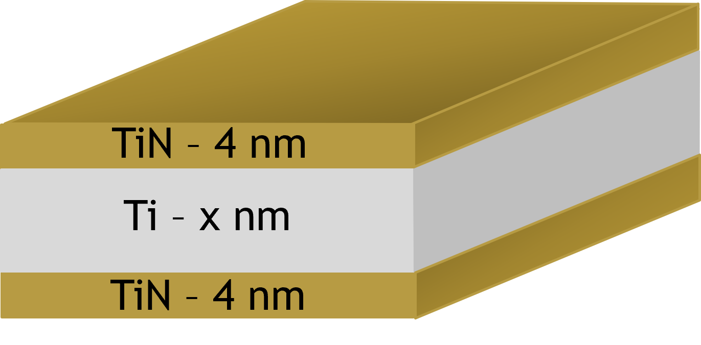

All the films reported here have been deposited so that both the top and bottom TiN layers are nominally 4 nm thick as described in Figure 1 (Left), while the Ti layer varies. Figure 1 (Right) shows that by changing the thickness of the sandwiched Ti layer, it is possible to accurately control the critical temperature of the multilayered film continuously between the critical temperature of pure Ti and that of stoichiometric TiN.
It proved impossible to distinguish the Ti from the TiN layers through Scanning Electron Microscopy (SEM), however control over the thickness of the individual layers can be inferred through the characterisation of the critical temperature of the wafers. Information on the reproducibility of the critical temperature of the films can be indirectly regarded as information on the control and reproducibility of the thickness of each individual layer. Experiments carried out on wafers with nominal thickness 4 nm, 10 nm and 4 nm for the bottom TiN, the Ti and the top TiN layers respectively, showed good reproducibility within 100 mK of the target critical temperature (1.60 K). Figure 2 shows the critical temperature of three samples from two different wafers measured. The three curves represent the range in which the critical temperature of a film with such nominal thickness values would reasonably lie. The red curve represents the superconducting at the highest critical temperature recorded, the blue one is for the coldest and the black one indicates the behaviour of the nominal film.

4 SINGLE WAFER UNIFORMITY
We next discuss how local and global inhomogeneities can affect the performance of an MKIDs array, in particular how a non-homogeneous film might account for an array with reduced pixel yield.
The sheet inductance of the thin film is a critical parameter for MKIDs. All of the resonators on the array are designed based on the assumption that the sheet inductance is constant across the full size of the chip. A variation in the sheet inductance of the superconductor results in a unpredictable variation in resonance frequency according to , and . Here, Lg represents the geometric inductance of the physical circuit and Lk represents the kinetic inductance, which is an inherent property of the superconducting resonator and depends on the sheet inductance of the film. This variation could take the form of an abrupt local variation or a slow radial gradient across the diameter of the wafer.
The sheet inductance of a superconductor can be described through a simple approach that follows the discussion found in Annunziata et al. [22] and Thinkam’s Introduction To Superconductivity [21]. Given a superconducting element of length , width , and thickness cooled down to a temperature and taking as Boltzmann’s constant, Equation 1 shows how the sheet inductance of a superconducting element depends on its dimensions, in particular its thickness, and its normal-state sheet resistance as well as its critical temperature .
| (1) |
Under the assumption that the critical temperature of the film does not vary too much across a 4 inch wafer, an assumption that we will further discuss later, we investigated how uniform the resistivity is across the wafer. This was achieved through 4-point Van Der Pauw measurements. The experimental setup is shown in Figure 3. The sample was wire bonded to the Van Der Pauw setup and the resistance measurements, performed in the dark, were performed with a SRS 921 resistance bridge.
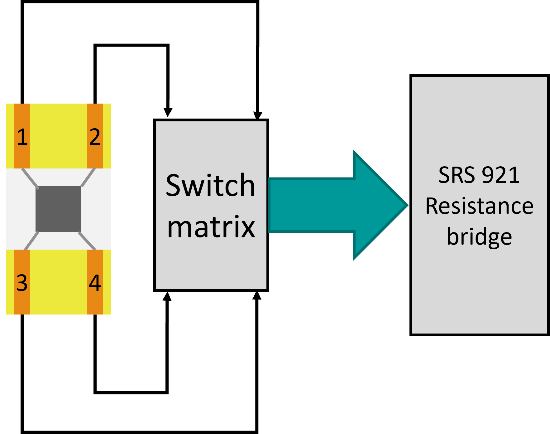
The sample preparation was rather simple. A 4 inch wafer was diced according to a 1 cm 1 cm square grid. Of all the samples thus produced, only the 60 inner ones, i.e. the ones with four straight edges, were taken into consideration for Van Der Pauw measurements. Van Der Pauw method correlates the resistance of the sample under examination with the sheet resistance of the thin film which appears in Equation 1.
This way, we produced the sheet resistance map in Figure 4 (Left) and a map which shows the variation of the sheet resistance of each individual square, from the average value (Right).


The map shows an average sheet resistance of with variation across the wafer that are smaller than . The accuracy of our measurements is within .
In order to justify the previous assumption that the critical temperature of the film is rather uniform across the 4 Inch wafer, we have identified 10 square samples of interest (Figure 5 (left): seven across two perpendicular radii (3,7,11,12,13,14,15) and three further squares that were regarded as particularly interesting because of large variations in resistivity as per the previous Van Der Pauw measurements (36,50,58). All ten chiplets exhibited a critical temperature of 1.70 K 0.01 mK (Figure 5 (Right)), which validates our previous assumption and suggests that the relative thicknesses of the 3 layers do not vary significantly across the 4” wafer. This will be further investigated through SEM scans.


5 MODELLING
5.1 Fabrication Yield
The fabrication of the detectors for such instruments is most often performed in research-grade clean rooms, through processes which are almost completely human-controlled and not automated. These processes have plenty of room for optimisation, although the fraction of non-responding pixels is less than .
Two or more resonators that resonate too near in frequency when they were not designed for this purpose, are said to be clashing or colliding. It is expected that random variations in the normal state sheet resistance of the superconductor (Rs) can have a detrimental impact on the fabrication yield.
The current state of the art is that most arrays exhibit a fabrication yield of and only for the best ones it goes as high as [10].
The model here discussed is based off the approach described by Liu et al.[23].
This simple model relies on a few basic assumptions:
- 1.
the array of resonators is infinite on both sides of resonator
- 2.
the distance, in frequency space, between two adjacent resonators is designed to be: MHz
- 3.
the n-th MKID’s resonance frequency is randomly distributed about according to a Gaussian distribution
- 4.
given a defined window size, a resonator that falls within said distance of any other resonator is said to be clashing.

The probability that the th resonator does not clash with the nth resonator, Pn0, can be evaluated, according to Liu et al.[23] as shown in equation 2, as one minus the overlapping area defined by the gaussian distribution and the collision window as described in Figure 6. Furthermore, due to the translation symmetry of the model, it is only necessary to evaluate Pn0 for all values of .
| (2) |
Where the integral of a Gaussian is evaluated through the error function Erf(x) defined as in Equation 3
| (3) |
Here, is the nominal spacing between the resonators ( = 2 MHz is a standard choice [3]) , and identifies the collision window through two parameters: represents the resonator’s line-width and a is assumed under the hypothesis that the resonators are well distinguishable when separated by line-widths. This is to say that the profile of the -th resonator is well contained in a window five times larges than its typical line-width.
Assuming all the resonators to be independent, the total yield is derived as:
| (4) |
The assumption of an infinite array allows to identify the probability presented in equation 4 with the total yield of the array.
For the sake of a model, it was assumed that the MKID resonates at the central frequency of the working bandwidth, GHz. And only the first resonators left and right have been taken into consideration. Equation 4 is only valid in the case of an infinite array of evenly spaced resonators.
The analysis of this model will be carried out in the next sections and the dependencies of the yield from physical parameters such as the quality factor of the resonators and the normal state sheet resistance of the superconductor will be investigated. It is worth observing that while increasing the spacing between two consecutive elements of the array, the yield increases accordingly.
5.2 Effects of the sheet resistivity
Given the change in kinetic inductance, and knowing that the resonance frequency of an LC circuit the fractional frequency shift in resonance frequency induced by a change in sheet resistance Rs, therefore a local change in kinetic inductance, is easily obtained provided three simplifying assumptions are met:
- 1.
The capacitance of the resonator is only due to its geometry
- 2.
The inductance is only due to the kinetic inductance. The kinetic inductance fraction
- 3.
Any variation in critical temperature Tc0 across the wafer is negligible.
Under these circumstances, the fractional frequency shift is given by Equation 5
| (5) |
The main purpose of this calculation is to try and estimate reasonable boundaries for the width of the distribution of the frequencies about their mean value . Given the biggest deviation we have observed in sheet resistance, as described in the previous section, one can conclude that . It is possible to identify the change in resonance frequency given by such a large variation in sheet resistance, as the value at 3. Such a non uniformity in Rs, under these assumptions, yield a value for of 120 kHZ.
5.3 Fabrication yield - results
It is important to discuss the results of the model previously described. The higher total quality factor of the resonators, the sharper is the resonator’s dip. is therefore inversely proportional to the line-width where is the characteristic resonant frequency.
Assuming a MHz, and based on formula 4, Figure 7 shows a 2D plot of the fabrication yield as a function of both and . Two trends are visible in the plot. The yield increases with increasing quality; this says that the sharper the resonator, hence the smaller their line-width and the clashing window, the higher the fabrication yield is. Also, as expected, the smaller the width of the frequency scatter distribution, the higher the yield per fixed values of .
Very strongly coupled resonators with low quality factors, such as , represent the case where the resonator’s rejection window is intrinsically larger than the spacing reducing dramatically the yield to a mathematical zero based on previous assumptions. For very high values of , the model is, in fact, describing an almost random distribution of resonant frequencies. It therefore makes sense that the yield becomes proportional to the rejection window size, thus to the total quality factor .

There are two main issues to address: first of all, a gargantuan value of would produce a yield as it would scatter most of the resonators outside the working-bandwidth, GHz. It was observed that the yield starts increasing from GHz onward. Another limit of the model is that, when evaluating the probability of a collision, only one of the two resonator’s dips is broadened, while the other is still regarded as if it was infinitely sharp. This effect is only relevant for very strongly coupled resonators, , therefore it is not significant for the plot in Figure 7. Further improvement, which is a higher-order approximation to what has been discussed so far resides in the evaluation of the line-width as a function of the specific resonator’s resonance frequency.
In order to summarise the results described in the previous pages, Table 2 represents some numerical results for interesting values of uniformity ( ) and total quality factor () .
| Yield (%) | ||
|---|---|---|
| 0.01 | 20000 | 99.9 |
| 0.06 | 20000 | 94.8 |
| 0.10 | 20000 | 83.5 |
| 0.15 | 20000 | 70.7 |
| 0.01 | 30000 | |
| 0.06 | 30000 | 99.9 |
| 0.10 | 30000 | 97.5 |
| 0.15 | 30000 | 88.6 |
| 0.01 | 50000 | |
| 0.06 | 50000 | |
| 0.10 | 50000 | 97.9 |
| 0.15 | 50000 | 95.8 |
| 0.01 | 100000 | |
| 0.06 | 100000 | |
| 0.10 | 100000 | 99.6 |
| 0.15 | 100000 | 98.4 |
6 CONCLUSIONS
In this paper we have characterised TiN/Ti/TiN multilayers with particular interest in their possible application for Microwave Kinetic Inductance Detectors. We demonstrated the possibility of controlling the critical temperature of the multilayer by changing the thickness of the Ti layer. Building on these results, we investigated the uniformity of our superconducting thin films. We have demonstrated that the normal state sheet resistance of the thin film, when measured at room temperature, is uniform within of its average value. In terms of critical temperature, we have not observed any significant variation within the resolution of our instruments.
Finally, we developed a model in order to predict how a variation in resistivity of the thin film affects the pixel yield of an MKIDs array.
We found out that, when no other effects come into play, an array of 2000 resonators evenly spaced by 2 MHz can exhibit a pixel yield of 94.8 when the resonators exhibit a total quality factor Qtot of 20000, or more for even higher .
Acknowledgements.
This publication has emanated from research conducted with the financial support of Science Foundation Ireland under Grant number 15/IA/2880. We would like to also thank the Process & Product Development team at Tyndall National Institute for providing wafer-processing services to fabricate the devicesReferences
- [1] Ulbricht, G., De Lucia, M., and Baldwin, E., “Applications for microwave kinetic induction detectors in advanced instrumentation,” Applied Sciences 11, 2671 (Mar 2021).
- [2] Walter, A., Mazin, B. B., Bockstiegel, C., Fruitwala, N., Szypryt, P., Lipartito, I., Meeker, S., Zobrist, N., Collura, G., Coiffard, G., Strader, P., Guyon, O., Lozi, J., and Jovanovic, N., “MEC: the MKID exoplanet camera for high contrast astronomy at Subaru (Conference Presentation),” in [Ground-based and Airborne Instrumentation for Astronomy VII ], Evans, C. J., Simard, L., and Takami, H., eds., 10702, International Society for Optics and Photonics, SPIE (2018).
- [3] Meeker, S. R., DARKNESS: The First Microwave Kinetic Inductance Detector Integral Field Spectrograph for Exoplanet Imaging, PhD thesis, University of California, Santa Barbara (2017).
- [4] Mazin, B. A., Meeker, S. R., Strader, M. J., Szypryt, P., Marsden, D., van Eyken, J. C., Duggan, G. E., Walter, A. B., Ulbricht, G., Johnson, M., and et al., “Arcons: A 2024 pixel optical through near-ir cryogenic imaging spectrophotometer,” Publications of the Astronomical Society of the Pacific 125, 1348–1361 (Nov 2013).
- [5] Baselmans, J., Bosma, S., Ikarashi, S., Klapwijk, T., Llombart, N., Pascual Laguna, A., Thoen, D., de Visser, P., Yurduseven, O., Endo, A., and More Authors, “Deshima on aste: On-sky responsivity calibration of the integrated superconducting spectrometer,” Journal of Low Temperature Physics 199(1-2), 231–239 (2020). Green Open Access added to TU Delft Institutional Repository ‘You share, we take care!’ – Taverne project https://www.openaccess.nl/en/you-share-we-take-care Otherwise as indicated in the copyright section: the publisher is the copyright holder of this work and the author uses the Dutch legislation to make this work public.
- [6] Austermann, J. E., Beall, J. A., Bryan, S. A., Dober, B., Gao, J., Hilton, G., Hubmayr, J., Mauskopf, P., McKenney, C. M., Simon, S. M., Ullom, J. N., Vissers, M. R., and Wilson, G. W., “Millimeter-wave polarimeters using kinetic inductance detectors for toltec and beyond,” Journal of Low Temperature Physics 193, 120–127 (May 2018).
- [7] Arnaboldi, C., Avignone, F., Balata, M., Barucci, M., Beeman, J., Brofferio, C., Bucci, C., Capelli, S., Carbone, L., Cebrian, S., Cremonesi, O., Creswick, R. J., Farach, H. A., Fiorini, E., Frossati, G., Giuliani, A., Haller, E. E., Irastorza, I. G., McDonald, R. J., Morales, A., Norman, E. B., Nucciotti, A., Palmieri, V., Pavan, M., Pedretti, M., Pessina, G., Pirro, S., Pobes, C., Previtali, E., Smith, A. R., Vanzini, M., Ventura, G., de Waard, A., and Zanotti, L., “The cuore experiment,” AIP Conference Proceedings 605(1), 469–472 (2002).
- [8] Colantoni, I., Cardani, L., Casali, N., Cruciani, A., Bellini, F., Castellano, M., Cosmelli, C., D’Addabbo, A., Di Domizio, S., Martinez, M., Tomei, C., and Vignati, M., “Design and Fabrication of the Second-Generation KID-Based Light Detectors of CALDER,” Journal of Low Temperature Physics 193, 726–731 (Dec. 2018).
- [9] Day, P. K., LeDuc, H. G., Mazin, B. A., Vayonakis, A., and Zmuidzinas, J., “A broadband superconducting detector suitable for use in large arrays,” Nature 425(6960), 817–821 (2003).
- [10] Mazin, B. A., Bailey, J., Bartlett, J., Bockstiegel, C., Bumble, B., Coiffard, G., Currie, T., Daal, M., Davis, K., Dodkins, R., Fruitwala, N., Jovanovic, N., Lipartito, I., Lozi, J., Males, J., Mawet, D., Meeker, S., O’Brien, K., Rich, M., Smith, J., Steiger, S., Swimmer, N., Walter, A., Zobrist, N., and Zmuidzinas, J., “Optical and near-ir microwave kinetic inductance detectors (mkids) in the 2020s,” (2019).
- [11] Zmuidzinas, J., “Superconducting microresonators: Physics and applications,” Annual Review of Condensed Matter Physics 3(1), 169–214 (2012).
- [12] Lucia, M. D., Baldwin, E., Ulbricht, G., Bracken, C., Stamenov, P., and Ray, T. P., “Multiplexable frequency retuning of MKID arrays using their non-linear kinetic inductance,” in [X-Ray, Optical, and Infrared Detectors for Astronomy IX ], Holland, A. D. and Beletic, J., eds., 11454, 580 – 590, International Society for Optics and Photonics, SPIE (2020).
- [13] Szypryt, P., [Development of Microwave Kinetic Inductance Detectors for Applications in Optical to Near-IR Astronomy ], UCSB (2017).
- [14] Baselmans, J. J. A. and Yates, S. J. C., “Long quasiparticle lifetime in aluminum microwave kinetic inductance detectors using coaxial stray light filters,” AIP Conference Proceedings 1185(1), 160–163 (2009).
- [15] Mazin, B. A., [Microwave Kinetic Inductance Detectors ], California Institute of Technology (2004).
- [16] Saveskul, N., Titova, N., Baeva, E., Semenov, A., Lubenchenko, A., Saha, S., Reddy, H., Bogdanov, S., Marinero, E., Shalaev, V., Boltasseva, A., Khrapai, V., Kardakova, A., and Goltsman, G., “Superconductivity behavior in epitaxial tin films points to surface magnetic disorder,” Physical Review Applied 12 (Nov 2019).
- [17] Vissers, M. R., Gao, J., Kline, J. S., Sandberg, M., Weides, M. P., Wisbey, D. S., and Pappas, D. P., “Characterization and in-situ monitoring of sub-stoichiometric adjustable superconducting critical temperature titanium nitride growth,” Thin Solid Films 548, 485–488 (Dec 2013).
- [18] Gao, J., Vissers, M. R., Sandberg, M. O., da Silva, F. C. S., Nam, S. W., Pappas, D. P., Wisbey, D. S., Langman, E. C., Meeker, S. R., Mazin, B. A., Leduc, H. G., Zmuidzinas, J., and Irwin, K. D., “A titanium-nitride near-infrared kinetic inductance photon-counting detector and its anomalous electrodynamics,” Applied Physics Letters 101, 142602 (oct 2012).
- [19] Sundgren, J.-E., “Structure and properties of tin coatings,” Thin Solid Films 128(1), 21–44 (1985).
- [20] Vissers, M. R., Gao, J., Sandberg, M., Duff, S. M., Wisbey, D. S., Irwin, K. D., and Pappas, D. P., “Proximity-coupled ti/tin multilayers for use in kinetic inductance detectors,” Applied Physics Letters 102(23), 232603 (2013).
- [21] Tinkham, M., [Introduction to Superconductivity ], Dover Publications, 2 ed. (June 2004).
- [22] Annunziata, A. J., Santavicca, D. F., Frunzio, L., Catelani, G., Rooks, M. J., Frydman, A., and Prober, D. E., “Tunable superconducting nanoinductors,” Nanotechnology 21, 445202 (Oct 2010).
- [23] Liu, X., Guo, W., Wang, Y., Dai, M., Wei, L. F., Dober, B., McKenney, C. M., Hilton, G. C., Hubmayr, J., Austermann, J. E., Ullom, J. N., Gao, J., and Vissers, M. R., “Superconducting micro-resonator arrays with ideal frequency spacing,” Applied Physics Letters 111(25), 252601 (2017).