Spin-orbit and exchange proximity couplings in graphene/1T-TaS2 heterostructure triggered by a charge density wave
Abstract
Proximity-induced fine features and spin-textures of the electronic bands in graphene-based van der Waals heterostructures can be explored from the point of tailoring a twist angle. Here we study spin-orbit coupling and exchange coupling engineering of graphene states in the proximity of 1T-TaS2 not triggering the twist, but a charge density wave in 1T-TaS2—a realistic low-temperature phase. Using density functional theory and effective model we found that the emergence of the charge density wave in 1T-TaS2 significantly enhances Rashba spin-orbit splitting in graphene and tilts the spin texture by a significant Rashba angle—in a very similar way as in the conventional twist-angle scenarios. Moreover, the partially filled Ta -band in the charge density wave phase leads to the spontaneous emergence of the in-plane magnetic order that transgresses via proximity from 1T-TaS2 to graphene, hence, simultaneously superimposing along the spin-orbit also the exchange coupling proximity effect. To describe this intricate proximity landscape we have developed an effective model Hamiltonian and provided a minimal set of parameters that excellently reproduces all the spectral features predicted by the first-principles calculations. Conceptually, the charge density wave provides a highly interesting knob to control the fine features of electronic states and to tailor the superimposed proximity effects—a sort of twistronics without twist.
August 11, 2026
1 Introduction
The ability to stack two-dimensional materials offers to design ultrathin van der Waals heterostructures [1, 2, 3] that can foster spintronics [4, 5, 6, 7, 8, 9], optoelectronics [10, 9, 11], and twistronics [12, 13] applications and pave the way to novel carbon-based and, hence, environmentally-friendly devices. Modifying the properties of van der Waals materials through proximity effects is an added degree of functionality so far very intensively explored, particularly, proximitizing graphene leads to the appearance of induced spin-orbit coupling (SOC) [10], or inducing magnetic exchange proximity effects [14, 15].
In order to add a novel tuning knob to the van der Waals heterostructures, we investigate the effect of charge density wave (CDW) that develops in 1T-TaS2 and explore its effect on the spin degree of freedom in proximitized graphene. In addition to various CDW orderings that are emerging in layered 3D bulk structures of transition metal dichalcogenides (TMDC) [16], also their 2D counterparts [17, 18, 19] offer a potential platform for studying the effects stemming from the dimensionality, and CDW-triggered commensurability and shape-topography [20, 21]. In particular, some of TMDC in the 1T polymorph phase have the propensity to exhibit a variety of periodic lattice distortions [22]. Frequently, the Peierls instability gives rise to a stable low temperature periodic CDW phase with a triangular superlattice. Particular examples count 1T-TMDC such TaS2 [23, 24, 25], TaSe2 [25, 26, 27] and TaTe2 [25, 27] or NbS2 [28] and NbSe2 [29, 30, 31]. Structural CDW distortions have the form of David stars [32]—clusters of 13 transition metal atoms in which an excess electron is effectively trapped at the star center [33, 34, 35, 36, 37, 38]. What is particularly interesting, the commensurate CDW phase of TaS2 forming the superlattice of David stars [39] possesses below 180 K [40] enough electronic correlations [41] to develop the Mott phase [42, 43, 44, 45, 46] and even superconductivity under pressure [32, 47]. Formation of CDW in 1T-TaS2 results from the subtle interplay of lattice, orbital and spin degrees of freedom [48], along with the electron-phonon coupling [49, 50] which results in strongly localized electronic states near the Fermi level [51]. The anharmonic phonon-phonon interactions in 1T-TaS2 are predicted to stabilize CDW at elevated temperatures [52]. The correlations at low-temperatures lead to spin polarization and transform a monolayer of 1T-TaS2 into a magnetically polarized semiconductor [53] with in-plane magnetization [54]. Rich electronic properties of 1T-TaS2 can be engineered by the temperature [55, 56, 57, 58], pressure [59], electrical pulses [60, 61], electrical bias [62, 63], creation of domain electronic walls [64], insertion of adsorbates [65, 66], charge doping [67], substrate selection [68], strain [69, 70, 71], or laser light [72, 73, 74, 75]. All this gives the 1T-TaS2 monolayer a potential for 2D spintronics applications counting ionic field-effect transistor [76], logic gates and circuits [77], non-volatile memory devices [78, 79, 58], and others.
In addition to many promising studies of 1T-TaS2 in the bulk or monolayer form, also its various heterostructures have been considered in recent literature, including the experimental works on the heterostructures with 2H-TaS2 [80], 2H-MoSe2 and 2H-WSe2 [81], 2H-MoS2 [82], permalloy [83], h-BN [84] or black phosphorus [85], and also graphene [86, 87, 41, 88]. The latter is providing an ideal platform for investigating fine spectral features stemming from the proximity of graphene Dirac electrons to the correlated CDW phase.
The CDW degree of freedom present in 1T-TaS2 and its spatial topology provides a channel to control the proximity exchange coupling and spin-orbit coupling in graphene without any physical change in a twist of the heterostructure components, as the CDW phase can be manipulated locally, for example, by optical means [89, 90, 91], electrical pulses [78, 79], or just temperature and in a fully reversible manner. Such a feature has been only achieved in optical lattice analog to bilayer graphene [92]. Twisted graphene/TMDC heterostructures have been recently intensively studied [93, 94, 95, 96, 97] and control of the twist angle is of paramount importance for possible applications based on the design of spin-charge conversion utilizing the Rashba-Edelstein effect [8, 98, 91, 99, 100]. Here we show that the same level of functionality can be expected also for graphene/CDW states where the “role of the twist” is played by the spatial topology of CDW.
In the paper, we study the van der Waals heterostructure of graphene and 1T-TaS2 monolayer by means of first-principles calculations and propose an effective tight-binding model for graphene bands near the Dirac point extracting relevant model parameters. We found that the model parameters reflect induced spin-orbit coupling and exchange interaction proximity effects for transitions of the 1T-TaS2 monolayer from the normal to CDW state, and then to the ferromagnetic ground state achieved by gradually decreasing temperature.
2 Effective Model Hamiltonian
Based on a given structural symmetry one can derive a specific effective model Hamiltonian for graphene -bands [101, 102]. It has been noted [93, 94] that the most general form of the induced Rashba spin-orbit coupling term in twisted graphene/TMDC heterostructures that obeys time reversal and threefold rotation symmetries can be written as , where is the effective Rashba Hamiltonian, [103, 104] and , where are the Pauli matrices acting in sublattice space, while are the Pauli spin matrices for the spin degree of freedom. The Rashba angle originates from spin-orbit coupling matrix elements between -orbitals of metal atoms in TMDC [93] and in general, represents a sum of the geometric angle and the quantum phase [105]. The results provided below are given with respect to the ordered Bloch basis:
| (1) |
where the states are sublattice (A, B) and spin (, ) resolved, and the crystal momentum is measured from the point.
The corresponding effective Hamiltonian in the studied cases has symmetry, and its low energy expansion close to the K and K’ point is given as follows:
| (2) |
The orbital and spin proximity effects result in the following parameters: corresponds to the Dirac point offset with respect to the Fermi energy, is the staggered potential discriminating electronic states located at sublattice A and B, and are the sublattice-resolved spin-conserving next-nearest neighbor spin-orbit couplings, is the Rashba spin-orbit coupling parameter with phase angle . Moreover, orbital nearest neighbor hopping and the lattice constant complete the set of parameters for the Hamiltonian as those can be subjected to CDW distortion. We should mention that the sublattice-resolved SOC parameters can be expressed as and , where is conventionally called intrinsic, or Kane-Mele SOC.
The above-described Hamiltonian (2) was used to model graphene band structure in the vicinity of the K/K’ points for normal and CDW phase of 1T-TaS2. The model parameters were determined to fit the density functional theory (DFT) calculations. A partially filled band in the vicinity of the Fermi level tends to spin split [53] at low temperatures and strong correlations of the Ta -electrons play an important role in the positioning of the lower and upper Hubbard bands [106, 47, 56, 107, 87]. This has an effect on the emergence of the in-plane magnetic polarization of the 1T-TaS2 [54]. In order to describe the spin-orbit coupling and also the exchange proximity coupling of the graphene bands around the Dirac points—we model the magnetic interaction between graphene and 1T-TaS2 Hubbard band in terms of effective Zeeman-like interactions captured by the following Hamiltonian:
| (3) |
The effective Hamiltonian , independent of the valley, represents the coupling of a spin with the sublattice-resolved (subscripts A/B) in-plane magnetization that is parameterized by the amplitude and the angle between the -axis and the magnetization direction.
3 First-principles calculations details
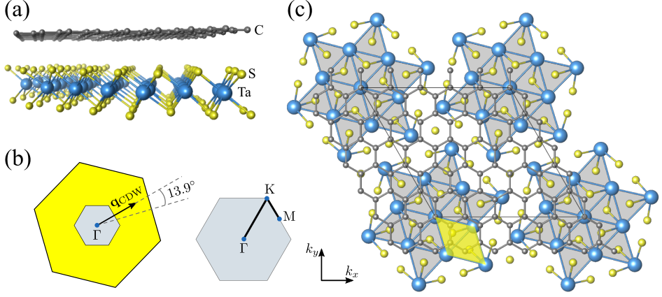
We consider a heterostructure with a structural model formed by the supercell of for 1T-TaS2 and for graphene, see Fig. 1. We study a slab geometry with a vacuum of about 15 in the direction perpendicular to the planes in order to separate periodic images. The graphene lattice parameter was compressed by approximately 1.4% to appropriately fit the supercell, capturing the commensurate CDW in 1T-TaS2, using the experimental lattice constant of 12.1323 Å [108]. The commensurate CDW can be described by a wavector whose orientation stems from the emerging of reconstruction and rotation angle of 13.9∘ [108, 109], see Fig. 1(b).
All the electronic structure calculations were performed using the Quantum Espresso suite [110, 111], implementing a plane wave basis for DFT calculations [112]. The Perdew-Burke-Ernzerhof exchange-correlation functional was utilized [113] for the projector augmented wave method [114]. For non-collinear DFT calculations including spin-orbit coupling, fully relativistic pseudopotentials were applied [115]. Small Methfessel-Paxton energy level smearing [116] of 1 mRy was used along with the kinetic energy cut-off of 53 Ry. The semiempirical van der Waals corrections were included [117, 118] and the dipole correction [119] was applied to properly determine Dirac point energy offset due to dipole electric field effects. The relaxation of atomic positions within the spin-unpolarized DFT approach was allowed with a threshold force of Ry per Bohr radius. For spin-polarized DFT+U calculations [120], we used on-site Hubbard eV for Ta -orbitals, inspired by the calculations reported in Refs. [21, 88], with mesh of -points used for sampling the first Brillouin zone.
4 Electronic band structures and results of fitting
We study two stacking configurations of graphene on 1T-TaS2, particularly, the top position where the carbon atom is placed over the Ta atom of the David star center and the hollow position where the center of graphene ring and the David star are placed on top of each other, see insets in Fig. 3. The CDW formation lowers the heterostructure energy per supercell by 152 meV for the top and by 136 meV for the hollow stacking, respectively. We note that those energies reasonably correspond to the transition of 1T-TaS2 to the commensurate CDW phase [32].
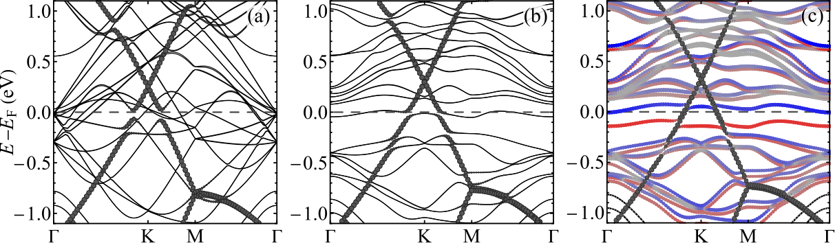
In Figure 2, we show calculated band structures of the supercell heterostructure for the top stacking along the high symmetry lines in the first Brillouin zone for the case where 1T-TaS2 is in the normal and in the CDW state (including the magnetic state, which we discuss in Section 5). The fat bands shown by the dark gray circles correspond to the states originating from the carbon atoms. The graphene gets hole-doped and its Dirac cone is shifted about 0.25 eV and 0.30 eV above the Fermi level for the normal and CDW phase, respectively. The -bands of graphene hybridize with the 1T-TaS2 states in the vicinity of the Fermi level. We note that in the case of the CDW phase, the bands of 1T-TaS2 significantly change and the Dirac states hybridize near the Fermi level with the partially filled Mott band originating predominantly from the orbitals of Ta atoms. The change in hybridization has a direct effect on proximity-induced spin-orbit coupling in graphene. The band structure for the hollow stacking (not shown) possesses on the energy scale as shown in Fig. 2 almost the same bands’ dispersion as the top stacked configuration. The bands differ noticeably in the vicinity of the Dirac point for two stackings in the CDW phase as will be seen from discussion of Fig. 3.
The Figure 3 shows details of the band structure topology of graphene in the vicinity of the Dirac point and corresponding , , and spin expectation values owing to proximity effects for the normal and CDW phase of 1T-TaS2. The calculated DFT results near the K point ( corresponds to the K point) are shown by circles while the solid lines are tight-binding model fits. Four different colours of these lines mark distinct bands in all the panels of the figure. In each case, both the electron and hole bands are spin split. For the normal phase at the top and hollow stacking, the band dispersions are electron-hole-like symmetric with significant band inversion and avoided crossings due to proximity-induced Rashba spin-orbit coupling. A similar band topology has been observed in the case of graphene on 1H-WSe2 leading to quantum spin Hall effect and pseudohelical states predicted in graphene nanoribbons [121, 122]. We note that in the normal phase, the and spin expectation values are identical for pairs of particle-hole symmetric bands, so that they overlap in the plots. Also, and spin expectation values vanish exactly at the K point for all cases considered in Fig. 3 due to the inherent symmetry. The emergence of CDW in the underlying 1T-TaS2 monolayer leads to the strong band topology modification due to a change in the spin-orbit coupling proximity-induced effects.
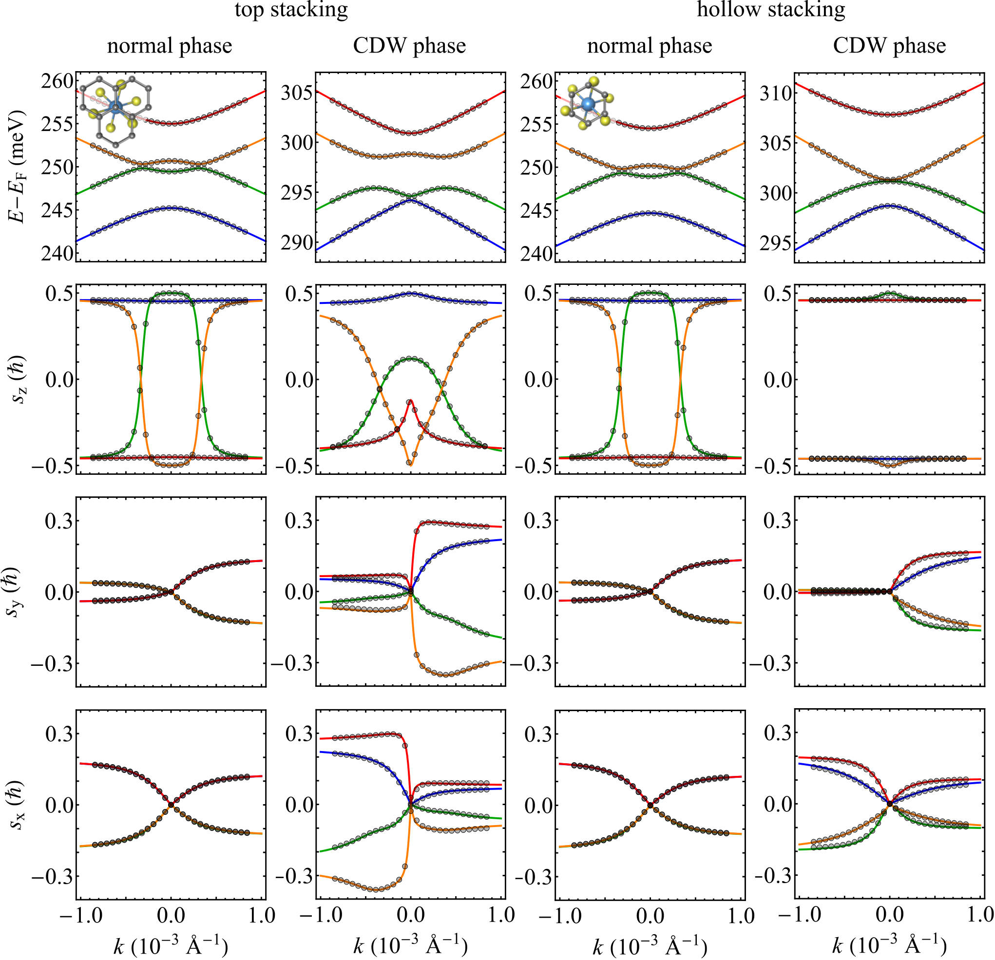
The complex features of the proximity-induced effects on graphene electronic structure can be studied by analyzing an effective tight-binding model. We used the Hamiltonian given by Eq. (2) and fit its parameters to the DFT data. The parameter values are summarized in Table 1 and provide a very good reproduction of the electronic band structure close to the Dirac point as well as the corresponding spin expectation values; compare DFT data (circles) and the tight-binding model (solid lines) in Fig. 3. The effect of the CDW phase in the case of top stacking leads to the band topologies mostly controlled by the sign change of the staggered potential and significant spin expectation values variation. In the case of hollow stacking with CDW, the bands’ dispersions are similar to the case of bare graphene in a strong transverse electric field which induces [123] and enforces the degeneracy of a pair of bands at the K point. However, in this case, the bands are nearly degenerate and the physical mechanism is more complex due to the presence of significant staggered potential and the sublattice-asymmetry of the intrinsic spin-orbit coupling (see the parameter values in Table 1). The most striking effect of the CDW phase is the enhancement of the Rashba angle in both stackings. This notably cants the in-plane spin components towards the radial direction, see Fig. 4 showing the behavior of the in-plane spin components along the circular contour in wavevector space at the distance of from the K point. It is noteworthy that each arrow color corresponds to an individual energy band as in Fig. 3. A somehow similar effect regarding the presence of a radial component of the Rashba field was predicted in twisted graphene/TMDC structures [94, 97, 105]. In the context of the enhancement of the Rashba angle by the emergence of CDW, let us emphasize the fundamental change in the band structure in the vicinity of Dirac point focusing on the bands originating from TaS2 (compare Fig. 2(a) and (b)). In the spirit of the model presented in Ref. [93] (discussing the case of a twisted heterostructure of graphene with TMDC), the change of the Rashba angle is a consequence of a pronounced difference between the TMDC energy band structure in the normal phase and the CDW phase.
| top stacking | hollow stacking | |||
| normal | CDW | normal | CDW | |
| (meV) | 250.08 | 297.13 | 249.57 | 302.24 |
| (eV) | 2.547 | 2.516 | 2.542 | 2.537 |
| (meV) | 1.90 | 1.30 | 1.91 | 2.13 |
| (meV) | 0.02 | 0.62 | 0.02 | 1.02 |
| (meV) | 2.52 | 1.85 | 2.52 | 2.06 |
| (meV) | 1.05 | 1.12 | 1.05 | 0.90 |
| (deg) | 17.36 | 43.07 | 17.57 | 28.15 |
5 Magnetism in graphene on 1T-TaS2 monolayer
The partially filled band at the Fermi level at the CDW phase of the 1T-TaS2 monolayer is suspected to indicate non-vanishing magnetic polarization according to recent first-principles studies [27, 54]. In order to study the presence of spontaneous magnetic polarization in graphene/1T-TaS2 monolayer, we have performed spin-polarized DFT+U calculations considering the CDW phase for 1T-TaS2. The stability of the magnetically ordered state can be evaluated by computing the energy difference between the non-magnetic and the magnetic ground state. Our DFT+U calculations yielded values (per supercell) equal to 34.7 meV and 33.1 meV for top and hollow stacking, respectively. On the other hand, analogous calculations performed for 1T-TaS2 monolayers with the graphene layer removed resulted in values of 29.8 meV and 28.2 meV, respectively. The results support the view that the creation of a heterostructure increases slightly the stability of the magnetic state in 1T-TaS2. For the calculations we have considered a preferential in-plane magnetization along the -direction, as we found that the magnetic anisotropy energy, i.e., the in-plane minus out-of-plane configuration energy (per supercell) amounts to 0.56 meV and 0.76 meV for top and hollow stacking, respectively, supporting the easy-plane anisotropy. The same type of anisotropy is predicted to emerge for a bare 1T-TaS2 monolayer with magnetic moments centered on David stars [54].
The band structure resulting from DFT+U calculations with CDW phase in 1T-TaS2 is shown in Fig. 2(c), where the fat bands originating from Ta atoms are marked with circles with color scale representing the degree of spin-polarization, linear color scale from red color for spin-up polarization, through gray to blue color for spin-down polarization. The main feature distinguishing this case from unpolarized CDW phase shown in Fig. 2(b) is pronounced spin splitting of the Hubbard flat Ta band located close to the Fermi level to a pair of strongly polarized bands. The remaining bands for the plotted energy range exhibit significantly lower degree of polarization.
| top stacking | hollow stacking | |
|---|---|---|
| (meV) | 336.50 | 336.16 |
| (eV) | 2.516 | 2.537 |
| (meV) | 1.81 | 2.27 |
| (meV) | 1.22 | 1.83 |
| (meV) | 1.98 | 2.47 |
| (meV) | 1.65 | 1.07 |
| (deg) | 56.90 | 30.93 |
| (meV) | 2.33 | 0.85 |
| (meV) | 1.66 | 0.74 |
| (deg) | 9.31 | 5.90 |
| (deg) | 3.86 | 20.37 |
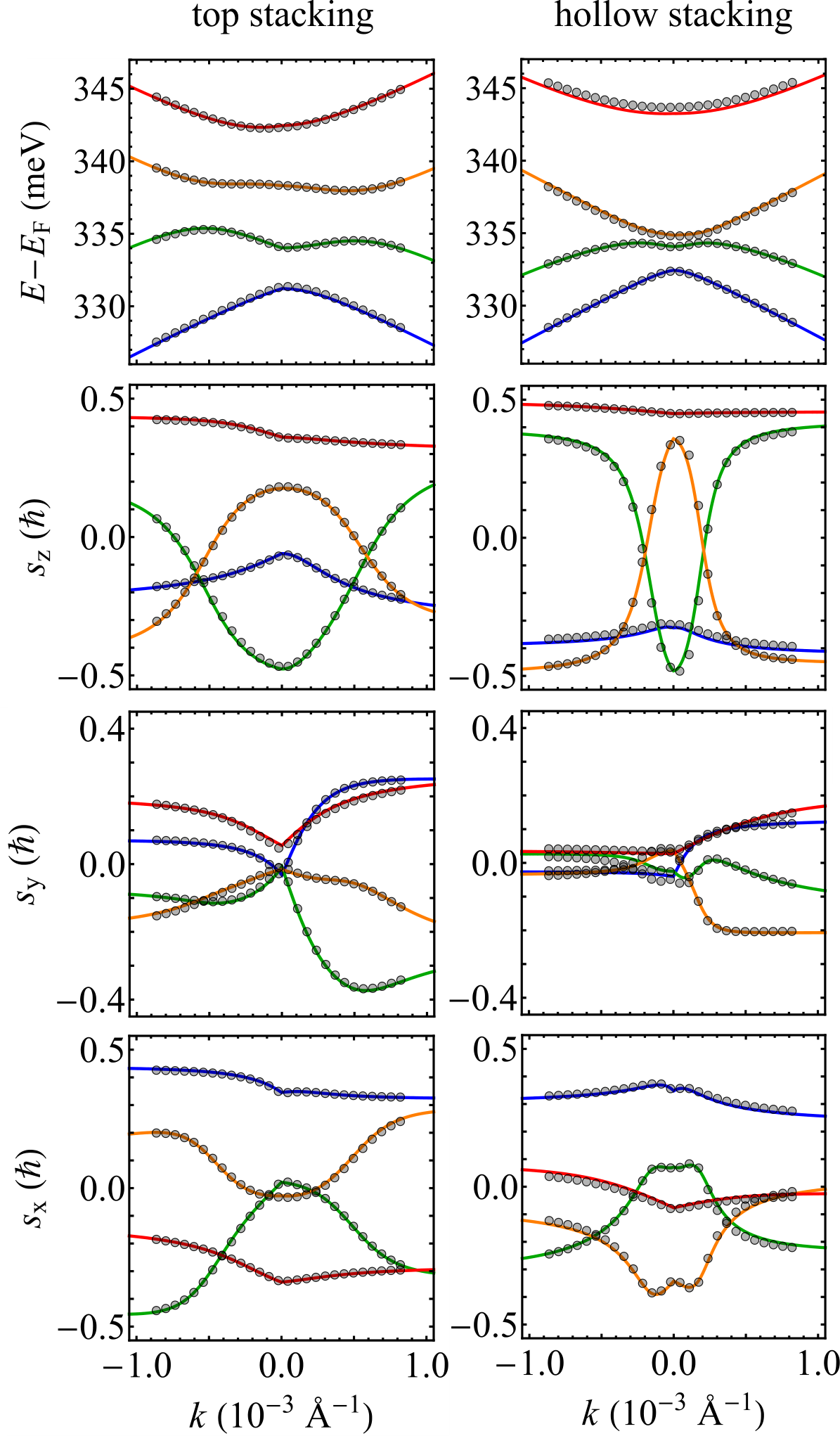
The effect of the in-plane magnetization on the graphene bands in the vicinity of the K/K’ point is well described by the effective Zeeman-like Hamiltonian , given by Eq. (3), representing the coupling of a spin with the sublattice-dependent in-plane magnetization, having the interaction strength and an angle with respect to the considered -direction. Using the Hamiltonian we were able to fit relativistic non-collinear DFT data. The obtained parameters are given in Table 2, while the comparison between the DFT and fitted data in Fig. 5 shows that the addition of the is able to capture the dominant behavior of the graphene bands in the vicinity of the K/K’ point when the magnetic polarization emerges. In both the top and the hollow stacking, the sublattice magnetization direction mostly points towards the -direction. It resembles the situation found in monolayer 1T-TaS2, in which the Mott-like band that lies on the Fermi level strongly contributes to the -component of magnetization [54]. The in-plane spin pattern, shown in Fig. 6, differs significantly from the one depicted in Fig. 4, for the non-magnetic case with CDW. The tilt angle shows pronounced angular dependence and, also, differs significantly for all four bands involved.
Our fitting shows that the presence of magnetism influences the graphene bands not only qualitatively through the appearance of the effective Zeeman-like Hamiltonian, but also quantitatively through the change of the nonmagnetic parameters of graphene Hamiltonian (Eq. (2)). This is not a surprise, since the exchange parameters of the order of 1 meV correspond to the giant built-in magnetic field of 17 T (see a comparison between the nonmagnetic data in Table 1 and magnetic data in Table 2), thus justifying the observed interference between the proximity-induced spin-orbit coupling and proximity-induced-magnetism. The effective model Hamiltonian we developed can be used in future studies probing interplays of several proximity-induced interactions, for instance, investigating spin-to-charge inter-conversion phenomena [124] or novel anisotropic Rashba-Edelstein effects that can be tuned by a twist [99] or by the engineering of CDW. The temperature in such cases can be used as an easy knob for switching between different phases and for turning on/off spin-orbit and exchange interactions.
6 Final remarks
In the paper, we report a study of the electronic properties of van der Waals graphene/1T-TaS2 heterostructure focusing on the proximity effects in the vicinity of the graphene Dirac point. The underlying band structures were computed by DFT calculations and then modeled analytically employing an effective tight-binding Hamiltonian derived from the symmetry considerations. The model parameters were determined by fitting the tight-binding to the DFT data. A crucial finding is the fundamental influence of CDW formation on the proximity effect, resulting in a profound change in the parameters, spin textures, and fine-band topologies. As a consequence, controlling the CDW presence in a heterostructure consisting of graphene on 1T-TaS2 provides a promising tool to manipulate the electronic properties of graphene near the Dirac point, in particular, a possibility to tailor the radial Rashba SOC, which cants the in-plane spin projections. In addition to SOC proximity, the in-plane magnetic polarization of the CDW phase superimposes the SOC, and exchange proximity effects offering to control the proximity effects by temperature.
Our findings demonstrate that the emergence of CDW in 1T-TaS2 profoundly modifies the proximity effects in the studied heterostructure with graphene. The effect bears resemblance to the physical situation in twisted heterostructures, where modification of the twist angle allows control over the proximity effects. It should be strongly emphasized that in our system this effect takes place without physical modification of the relative twist angle of 13.9∘ between the graphene layer and 1T-TaS2 layer, as enforced by the lattice commensurability for reconstruction. Therefore, a specific sort of spintronics/twistronics without a twist may be realized based on CDW control in our heterostructure.
The proximity-induced SOC controlled with the twist angle in van der Waals graphene/TMDC heterostructure might find application in spin-to-charge inter-conversion [125, 99]. In particular, the modification of the in-plane spin texture with the twist angle enables tunability of the Rashba-Edelstein effect [99]. In this context, we might mention that the controllability of the proximity effects in our heterostructure offers a route to master also the spin-to-charge inter-conversion but without the need to tune physically the twist angle and with full reversibility.
ORCID IDs:
Karol Szałowski: https://orcid.org/0000-0002-3204-1849
Marko Milivojević: https://orcid.org/0000-0002-9583-3640
Denis Kochan: https://orcid.org/0000-0003-0613-5996
Martin Gmitra: https://orcid.org/0000-0003-1118-3028
References
References
- [1] A. K. Geim, I. V. Grigorieva, Van der Waals heterostructures, Nature 499 (7459) (2013) 419–425. doi:10.1038/nature12385.
- [2] J. F. Sierra, J. Fabian, R. K. Kawakami, S. Roche, S. O. Valenzuela, Van der Waals heterostructures for spintronics and opto-spintronics, Nature Nanotechnology 16 (8) (2021) 856–868. doi:10.1038/s41565-021-00936-x.
- [3] H. Kurebayashi, J. H. Garcia, S. Khan, J. Sinova, S. Roche, Magnetism, symmetry and spin transport in van der Waals layered systems, Nature Reviews Physics 4 (3) (2022) 150–166. doi:10.1038/s42254-021-00403-5.
- [4] W. Han, R. K. Kawakami, M. Gmitra, J. Fabian, Graphene spintronics, Nature Nanotechnology 9 (10) (2014) 794–807. doi:10.1038/nnano.2014.214.
- [5] A. Avsar, J. Y. Tan, T. Taychatanapat, J. Balakrishnan, G. K. W. Koon, Y. Yeo, J. Lahiri, A. Carvalho, A. S. Rodin, E. C. T. O’Farrell, G. Eda, A. H. Castro Neto, B. Özyilmaz, Spin–orbit proximity effect in graphene, Nature Communications 5 (1) (2014) 4875. doi:10.1038/ncomms5875.
- [6] T.-R. T. Han, F. Zhou, C. D. Malliakas, P. M. Duxbury, S. D. Mahanti, M. G. Kanatzidis, C.-Y. Ruan, Exploration of metastability and hidden phases in correlated electron crystals visualized by femtosecond optical doping and electron crystallography, Science Advances 1 (5) (2015) e1400173. doi:10.1126/sciadv.1400173.
- [7] P. Wang, C. Jia, Y. Huang, X. Duan, Van der Waals Heterostructures by Design: From 1D and 2D to 3D, Matter 4 (2) (2021) 552–581. doi:10.1016/j.matt.2020.12.015.
- [8] R. Galceran, B. Tian, J. Li, F. Bonell, M. Jamet, C. Vergnaud, A. Marty, J. H. García, J. F. Sierra, M. V. Costache, S. Roche, S. O. Valenzuela, A. Manchon, X. Zhang, U. Schwingenschlögl, Control of spin–charge conversion in van der Waals heterostructures, APL Materials 9 (10) (2021) 100901. doi:10.1063/5.0054865.
- [9] M. Gmitra, J. Fabian, Proximity Effects in Bilayer Graphene on Monolayer WSe2: Field-Effect Spin Valley Locking, Spin-Orbit Valve, and Spin Transistor, Physical Review Letters 119 (14) (2017) 146401. doi:10.1103/PhysRevLett.119.146401.
- [10] M. Gmitra, J. Fabian, Graphene on transition-metal dichalcogenides: A platform for proximity spin-orbit physics and optospintronics, Physical Review B 92 (15) (2015) 155403. doi:10.1103/PhysRevB.92.155403.
- [11] W. Liao, Y. Huang, H. Wang, H. Zhang, Van der Waals heterostructures for optoelectronics: Progress and prospects, Applied Materials Today 16 (2019) 435–455. doi:10.1016/j.apmt.2019.07.004.
- [12] S. Carr, D. Massatt, S. Fang, P. Cazeaux, M. Luskin, E. Kaxiras, Twistronics: Manipulating the electronic properties of two-dimensional layered structures through their twist angle, Physical Review B 95 (7) (2017) 075420. doi:10.1103/PhysRevB.95.075420.
- [13] Z. Hennighausen, S. Kar, Twistronics: A turning point in 2D quantum materials, Electronic Structure 3 (1) (2021) 014004. doi:10.1088/2516-1075/abd957.
- [14] K. Zollner, M. Gmitra, T. Frank, J. Fabian, Theory of proximity-induced exchange coupling in graphene on hBN/(Co, Ni), Physical Review B 94 (15) (2016) 155441. doi:10.1103/PhysRevB.94.155441.
- [15] K. Zollner, P. E. Faria Junior, J. Fabian, Giant proximity exchange and valley splitting in transition metal dichalcogenide/hBN/(Co,Ni) heterostructures, Physical Review B 101 (8) (2020) 085112. doi:10.1103/PhysRevB.101.085112.
- [16] K. Rossnagel, On the origin of charge-density waves in select layered transition-metal dichalcogenides, Journal of Physics: Condensed Matter 23 (21) (2011) 213001. doi:10.1088/0953-8984/23/21/213001.
- [17] D. Lin, S. Li, J. Wen, H. Berger, L. Forró, H. Zhou, S. Jia, T. Taniguchi, K. Watanabe, X. Xi, M. S. Bahramy, Patterns and driving forces of dimensionality-dependent charge density waves in 2H-type transition metal dichalcogenides, Nature Communications 11 (1) (2020) 2406. doi:10.1038/s41467-020-15715-w.
- [18] Z. Xu, H. Yang, X. Song, Y. Chen, H. Yang, M. Liu, Z. Huang, Q. Zhang, J. Sun, L. Liu, Y. Wang, Topical review: Recent progress of charge density waves in 2D transition metal dichalcogenide-based heterojunctions and their applications, Nanotechnology 32 (49) (2021) 492001. doi:10.1088/1361-6528/ac21ed.
- [19] K. Lasek, J. Li, S. Kolekar, P. M. Coelho, L. Guo, M. Zhang, Z. Wang, M. Batzill, Synthesis and characterization of 2D transition metal dichalcogenides: Recent progress from a vacuum surface science perspective, Surface Science Reports 76 (2) (2021) 100523. doi:10.1016/j.surfrep.2021.100523.
- [20] A. S. Ngankeu, S. K. Mahatha, K. Guilloy, M. Bianchi, C. E. Sanders, K. Hanff, K. Rossnagel, J. A. Miwa, C. Breth Nielsen, M. Bremholm, P. Hofmann, Quasi-one-dimensional metallic band dispersion in the commensurate charge density wave of 1T-TaS2, Physical Review B 96 (19) (2017) 195147. doi:10.1103/PhysRevB.96.195147.
- [21] E. Martino, A. Pisoni, L. Ćirić, A. Arakcheeva, H. Berger, A. Akrap, C. Putzke, P. J. W. Moll, I. Batistić, E. Tutiš, L. Forró, K. Semeniuk, Preferential out-of-plane conduction and quasi-one-dimensional electronic states in layered 1T-TaS2, npj 2D Materials and Applications 4 (1) (2020) 1–9. doi:10.1038/s41699-020-0145-z.
- [22] D. Pasquier, O. V. Yazyev, Unified picture of lattice instabilities in metallic transition metal dichalcogenides, Physical Review B 100 (20) (2019) 201103. doi:10.1103/PhysRevB.100.201103.
- [23] J. Wilson, F. Di Salvo, S. Mahajan, Charge-density waves and superlattices in the metallic layered transition metal dichalcogenides, Advances in Physics 24 (2) (1975) 117–201. doi:10.1080/00018737500101391.
- [24] R. Brouwer, F. Jellinek, The low-temperature superstructures of 1T-TaSe2 and 2H-TaSe2, Physica B+C 99 (1) (1980) 51–55. doi:10.1016/0378-4363(80)90209-0.
- [25] D. C. Miller, S. D. Mahanti, P. M. Duxbury, Charge density wave states in tantalum dichalcogenides, Physical Review B 97 (4) (2018) 045133. doi:10.1103/PhysRevB.97.045133.
- [26] K. Zhang, C. Si, C.-S. Lian, J. Zhou, Z. Sun, Mottness collapse in monolayer 1T-TaSe2 with persisting charge density wave order, Journal of Materials Chemistry C 8 (28) (2020) 9742–9747. doi:10.1039/D0TC01719A.
- [27] T. Jiang, T. Hu, G.-D. Zhao, Y. Li, S. Xu, C. Liu, Y. Cui, W. Ren, Two-dimensional charge density waves in TaX2 (X=S,Se,Te) from first principles, Physical Review B 104 (7) (2021) 075147. doi:10.1103/PhysRevB.104.075147.
- [28] C. Tresca, M. Calandra, Charge density wave and spin 1/2 insulating state in single layer 1T-NbS2, 2D Materials 6 (3) (2019) 035041. doi:10.1088/2053-1583/ab23c0.
- [29] M. Calandra, Phonon-Assisted Magnetic Mott-Insulating State in the Charge Density Wave Phase of Single-Layer 1T-NbSe2, Physical Review Letters 121 (2) (2018) 026401. doi:10.1103/PhysRevLett.121.026401.
- [30] L. Liu, H. Yang, Y. Huang, X. Song, Q. Zhang, Z. Huang, Y. Hou, Y. Chen, Z. Xu, T. Zhang, X. Wu, J. Sun, Y. Huang, F. Zheng, X. Li, Y. Yao, H.-J. Gao, Y. Wang, Direct identification of Mott Hubbard band pattern beyond charge density wave superlattice in monolayer 1T-NbSe2, Nature Communications 12 (1) (2021) 1978. doi:10.1038/s41467-021-22233-w.
- [31] M. Liu, J. Leveillee, S. Lu, J. Yu, H. Kim, C. Tian, Y. Shi, K. Lai, C. Zhang, F. Giustino, C.-K. Shih, Monolayer 1T-NbSe2 as a 2D-correlated magnetic insulator, Science Advances 7 (47) (2021) eabi6339. doi:10.1126/sciadv.abi6339.
- [32] B. Sipos, A. F. Kusmartseva, A. Akrap, H. Berger, L. Forró, E. Tutiš, From Mott state to superconductivity in 1T-TaS2, Nature Materials 7 (12) (2008) 960–965. doi:10.1038/nmat2318.
- [33] E. Tosatti, P. Fazekas, ON THE NATURE OF THE LOW-TEMPERATURE PHASE OF 1T-TaS2, Le Journal de Physique Colloques 37 (C4) (1976) C4–168. doi:10.1051/jphyscol:1976426.
- [34] P. Fazekas, E. Tosatti, Electrical, structural and magnetic properties of pure and doped 1T-TaS2, Philosophical Magazine B 39 (3) (1979) 229–244. doi:10.1080/13642817908245359.
- [35] P. Fazekas, E. Tosatti, Charge carrier localization in pure and doped 1T-TaS2, Physica B+C 99 (1) (1980) 183–187. doi:10.1016/0378-4363(80)90229-6.
- [36] N. V. Smith, S. D. Kevan, F. J. DiSalvo, Band structures of the layer compounds 1T-TaS2 and 2H-TaSe2 in the presence of commensurate charge-density waves, Journal of Physics C: Solid State Physics 18 (16) (1985) 3175. doi:10.1088/0022-3719/18/16/013.
- [37] K. Rossnagel, N. V. Smith, Spin-orbit coupling in the band structure of reconstructed 1T-TaS2, Physical Review B 73 (7) (2006) 073106. doi:10.1103/PhysRevB.73.073106.
- [38] M. Kratochvilova, A. D. Hillier, A. R. Wildes, L. Wang, S.-W. Cheong, J.-G. Park, The low-temperature highly correlated quantum phase in the charge-density-wave 1T-TaS2 compound, npj Quantum Materials 2 (1) (2017) 1–7. doi:10.1038/s41535-017-0048-1.
- [39] T. Ritschel, J. Trinckauf, G. Garbarino, M. Hanfland, M. v. Zimmermann, H. Berger, B. Büchner, J. Geck, Pressure dependence of the charge density wave in 1T-TaS2 and its relation to superconductivity, Physical Review B 87 (12) (2013) 125135. doi:10.1103/PhysRevB.87.125135.
- [40] L. Perfetti, T. A. Gloor, F. Mila, H. Berger, M. Grioni, Unexpected periodicity in the quasi-two-dimensional Mott insulator 1T-TaS2 revealed by angle-resolved photoemission, Physical Review B 71 (15) (2005) 153101. doi:10.1103/PhysRevB.71.153101.
- [41] T. J. Kim, M. Y. Jeong, M. J. Han, Non-local Coulomb interaction and correlated electronic structure of TaS2: A GW+EDMFT study (Jun. 2022). arXiv:2206.08519, doi:10.48550/arXiv.2206.08519.
- [42] D. Shin, N. Tancogne-Dejean, J. Zhang, M. S. Okyay, A. Rubio, N. Park, Identification of the Mott Insulating Charge Density Wave State in 1T-TaS2, Physical Review Letters 126 (19) (2021) 196406. doi:10.1103/PhysRevLett.126.196406.
- [43] V. Petkov, J. E. Peralta, B. Aoun, Y. Ren, Atomic structure and Mott nature of the insulating charge density wave phase of 1T-TaS2, Journal of Physics: Condensed Matter 34 (34) (2022) 345401. doi:10.1088/1361-648X/ac77cf.
- [44] F. Petocchi, C. W. Nicholson, B. Salzmann, D. Pasquier, O. V. Yazyev, C. Monney, P. Werner, Mott versus Hybridization Gap in the Low-Temperature Phase of 1T-TaS2, Physical Review Letters 129 (1) (2022) 016402. doi:10.1103/PhysRevLett.129.016402.
- [45] Q.-H. Ren, T. Suzuki, T. Kanai, J. Itatani, S. Shin, K. Okazaki, Coexistence of the Charge-Density-Wave Phase in the Photo-Induced Metallic Phase in 1T-TaS2 (Jul. 2022). arXiv:2207.05232, doi:10.48550/arXiv.2207.05232.
- [46] Y. Fei, Z. Wu, W. Zhang, Y. Yin, Understanding the Mott insulating state in 1T-TaS2 and 1T-TaSe2, AAPPS Bulletin 32 (1) (2022) 20. doi:10.1007/s43673-022-00049-0.
- [47] P. Darancet, A. J. Millis, C. A. Marianetti, Three-dimensional metallic and two-dimensional insulating behavior in octahedral tantalum dichalcogenides, Physical Review B 90 (4) (2014) 045134. doi:10.1103/PhysRevB.90.045134.
- [48] S. Yi, Z. Zhang, J.-H. Cho, Coupling of charge, lattice, orbital, and spin degrees of freedom in charge density waves in 1T-TaS2, Physical Review B 97 (4) (2018) 041413. doi:10.1103/PhysRevB.97.041413.
- [49] G. Grüner, The dynamics of charge-density waves, Reviews of Modern Physics 60 (4) (1988) 1129–1181. doi:10.1103/RevModPhys.60.1129.
- [50] A. Y. Liu, Electron-phonon coupling in compressed 1T-TaS2: Stability and superconductivity from first principles, Physical Review B 79 (22) (2009) 220515. doi:10.1103/PhysRevB.79.220515.
- [51] C. Wen, J. Gao, Y. Xie, Q. Zhang, P. Kong, J. Wang, Y. Jiang, X. Luo, J. Li, W. Lu, Y.-P. Sun, S. Yan, Roles of the Narrow Electronic Band near the Fermi Level in 1T-TaS2-Related Layered Materials, Physical Review Letters 126 (25) (2021) 256402. doi:10.1103/PhysRevLett.126.256402.
- [52] P. Lazar, J. Martincová, M. Otyepka, Structure, dynamical stability, and electronic properties of phases in TaS2 from a high-level quantum mechanical calculation, Physical Review B 92 (22) (2015) 224104. doi:10.1103/PhysRevB.92.224104.
- [53] Q. Zhang, L.-Y. Gan, Y. Cheng, U. Schwingenschlögl, Spin polarization driven by a charge-density wave in monolayer 1T-TaS2, Physical Review B 90 (8) (2014) 081103. doi:10.1103/PhysRevB.90.081103.
- [54] D. Pasquier, O. V. Yazyev, Ab initio theory of magnetism in two-dimensional 1T-TaS2, Physical Review B 105 (8) (2022) L081106. doi:10.1103/PhysRevB.105.L081106.
- [55] I. Lutsyk, M. Rogala, P. Dabrowski, P. Krukowski, P. J. Kowalczyk, A. Busiakiewicz, D. A. Kowalczyk, E. Lacinska, J. Binder, N. Olszowska, M. Kopciuszynski, K. Szalowski, M. Gmitra, R. Stepniewski, M. Jalochowski, J. J. Kolodziej, A. Wysmolek, Z. Klusek, Electronic structure of commensurate, nearly commensurate, and incommensurate phases of 1T-TaS2 by angle-resolved photoelectron spectroscopy, scanning tunneling spectroscopy, and density functional theory, Physical Review B 98 (19) (2018) 195425. doi:10.1103/PhysRevB.98.195425.
- [56] Y. D. Wang, W. L. Yao, Z. M. Xin, T. T. Han, Z. G. Wang, L. Chen, C. Cai, Y. Li, Y. Zhang, Band insulator to Mott insulator transition in 1T-TaS2, Nature Communications 11 (1) (2020) 4215. doi:10.1038/s41467-020-18040-4.
- [57] A. Mohammadzadeh, A. Rehman, F. Kargar, S. Rumyantsev, J. M. Smulko, W. Knap, R. K. Lake, A. A. Balandin, Room temperature depinning of the charge-density waves in quasi-two-dimensional 1T-TaS2 devices, Applied Physics Letters 118 (22) (2021) 223101. doi:10.1063/5.0055401.
- [58] D. Mihailovic, D. Svetin, I. Vaskivskyi, R. Venturini, B. Lipovšek, A. Mraz, Ultrafast non-thermal and thermal switching in charge configuration memory devices based on 1T-TaS2, Applied Physics Letters 119 (1) (2021) 013106. doi:10.1063/5.0052311.
- [59] S.-H. Lee, J. S. Goh, D. Cho, Origin of the Insulating Phase and First-Order Metal-Insulator Transition in 1T-TaS2, Physical Review Letters 122 (10) (2019) 106404. doi:10.1103/PhysRevLett.122.106404.
- [60] M. J. Hollander, Y. Liu, W.-J. Lu, L.-J. Li, Y.-P. Sun, J. A. Robinson, S. Datta, Electrically Driven Reversible Insulator–Metal Phase Transition in 1T-TaS2, Nano Letters 15 (3) (2015) 1861–1866. doi:10.1021/nl504662b.
- [61] L. Ma, C. Ye, Y. Yu, X. F. Lu, X. Niu, S. Kim, D. Feng, D. Tománek, Y.-W. Son, X. H. Chen, Y. Zhang, A metallic mosaic phase and the origin of Mott-insulating state in 1T-TaS2, Nature Communications 7 (1) (2016) 10956. doi:10.1038/ncomms10956.
- [62] R. Zhao, B. Grisafe, R. K. Ghosh, S. Holoviak, B. Wang, K. Wang, N. Briggs, A. Haque, S. Datta, J. Robinson, Two-dimensional tantalum disulfide: Controlling structure and properties via synthesis, 2D Materials 5 (2) (2018) 025001. doi:10.1088/2053-1583/aaa104.
- [63] W. Li, G. V. Naik, Reorganization of CDW stacking in 1T-TaS2 by an in-plane electrical bias, APL Materials 9 (11) (2021) 111103. doi:10.1063/5.0069855.
- [64] D. Cho, G. Gye, J. Lee, S.-H. Lee, L. Wang, S.-W. Cheong, H. W. Yeom, Correlated electronic states at domain walls of a Mott-charge-density-wave insulator 1T-TaS2, Nature Communications 8 (1) (2017) 392. doi:10.1038/s41467-017-00438-2.
- [65] J. Lee, K.-H. Jin, A. Catuneanu, A. Go, J. Jung, C. Won, S.-W. Cheong, J. Kim, F. Liu, H.-Y. Kee, H. W. Yeom, Honeycomb-Lattice Mott Insulator on Tantalum Disulphide, Physical Review Letters 125 (9) (2020) 096403. doi:10.1103/PhysRevLett.125.096403.
- [66] D. Lee, K.-H. Jin, F. Liu, H. W. Yeom, Tunable Mott Dirac and Kagome Bands Engineered on 1T-TaS2, Nano Letters 22 (19) (2022) 7902–7909. doi:10.1021/acs.nanolett.2c02866.
- [67] D. F. Shao, R. C. Xiao, W. J. Lu, H. Y. Lv, J. Y. Li, X. B. Zhu, Y. P. Sun, Manipulating charge density waves in 1T-TaS by charge-carrier doping: A first-principles investigation, Physical Review B 94 (12) (2016) 125126. doi:10.1103/PhysRevB.94.125126.
- [68] R. Zhao, Y. Wang, D. Deng, X. Luo, W. J. Lu, Y.-P. Sun, Z.-K. Liu, L.-Q. Chen, J. Robinson, Tuning Phase Transitions in 1T-TaS2 via the Substrate, Nano Letters 17 (6) (2017) 3471–3477. doi:10.1021/acs.nanolett.7b00418.
- [69] L.-Y. Gan, L.-H. Zhang, Q. Zhang, C.-S. Guo, U. Schwingenschlögl, Y. Zhao, Strain tuning of the charge density wave in monolayer and bilayer 1T-TaS2, Physical Chemistry Chemical Physics 18 (4) (2016) 3080–3085. doi:10.1039/C5CP05695K.
- [70] K. Bu, W. Zhang, Y. Fei, Z. Wu, Y. Zheng, J. Gao, X. Luo, Y.-P. Sun, Y. Yin, Possible strain induced Mott gap collapse in 1T-TaS2, Communications Physics 2 (1) (2019) 1–7. doi:10.1038/s42005-019-0247-0.
- [71] C. W. Nicholson, F. Petocchi, B. Salzmann, C. Witteveen, M. Rumo, G. Kremer, F. O. von Rohr, P. Werner, C. Monney, Modified interlayer stacking and insulator to correlated-metal transition driven by uniaxial strain in 1T-TaS2 (Apr. 2022). arXiv:2204.05598, doi:10.48550/arXiv.2204.05598.
- [72] L. Stojchevska, I. Vaskivskyi, T. Mertelj, P. Kusar, D. Svetin, S. Brazovskii, D. Mihailovic, Ultrafast Switching to a Stable Hidden Quantum State in an Electronic Crystal, Science 344 (6180) (2014) 177–180. doi:10.1126/science.1241591.
- [73] K. Ludwiczak, E. Lacinska, J. Binder, I. Lutsyk, M. Rogala, P. Dabrowski, Z. Klusek, R. Stepniewski, A. Wysmolek, Impeded phase transition in 1T-TaS2: Thermoelectric fingerprint of long-lived mixed states, Solid State Communications 305 (2020) 113749. doi:10.1016/j.ssc.2019.113749.
- [74] E. M. Lacinska, M. Furman, J. Binder, I. Lutsyk, P. J. Kowalczyk, R. Stepniewski, A. Wysmolek, Raman Optical Activity of 1T-TaS2, Nano Letters 22 (7) (2022) 2835–2842. doi:10.1021/acs.nanolett.1c04990.
- [75] Q.-H. Ren, T. Suzuki, T. Kanai, J. Itatani, S. Shin, K. Okazaki, Dynamical swinging between the insulating and metallic phases induced by the coherent amplitude mode excitation in 1T-TaS2, Preprint available at Research Square [https://doi.org/10.21203/rs.3.rs-2441185/v1] (Jan. 2023). doi:10.21203/rs.3.rs-2441185/v1.
- [76] Y. Yu, F. Yang, X. F. Lu, Y. J. Yan, Y.-H. Cho, L. Ma, X. Niu, S. Kim, Y.-W. Son, D. Feng, S. Li, S.-W. Cheong, X. H. Chen, Y. Zhang, Gate-tunable phase transitions in thin flakes of 1T-TaS2, Nature Nanotechnology 10 (3) (2015) 270–276. doi:10.1038/nnano.2014.323.
- [77] A. G. Khitun, A. K. Geremew, A. A. Balandin, Transistor-Less Logic Circuits Implemented With 2-D Charge Density Wave Devices, IEEE Electron Device Letters 39 (9) (2018) 1449–1452. doi:10.1109/LED.2018.2858244.
- [78] I. Vaskivskyi, J. Gospodaric, S. Brazovskii, D. Svetin, P. Sutar, E. Goreshnik, I. A. Mihailovic, T. Mertelj, D. Mihailovic, Controlling the metal-to-insulator relaxation of the metastable hidden quantum state in 1T-TaS2, Science Advances 1 (6) (2015) e1500168. doi:10.1126/sciadv.1500168.
- [79] I. Vaskivskyi, I. A. Mihailovic, S. Brazovskii, J. Gospodaric, T. Mertelj, D. Svetin, P. Sutar, D. Mihailovic, Fast electronic resistance switching involving hidden charge density wave states, Nature Communications 7 (1) (2016) 11442. doi:10.1038/ncomms11442.
- [80] C. G. Ayani, M. Pisarra, I. M. Ibarburu, M. Garnica, R. Miranda, F. Calleja, F. Martín, A. L. V. de Parga, Two-dimensional Kondo lattice in a TaS2 van der Waals heterostructure (May 2022). arXiv:2205.11383, doi:10.48550/arXiv.2205.11383.
- [81] J. Lee, J. Bang, J. Kang, Nonequilibrium Charge-Density-Wave Melting in 1T-TaS2 Triggered by Electronic Excitation: A Real-Time Time-Dependent Density Functional Theory Study, The Journal of Physical Chemistry Letters 13 (25) (2022) 5711–5718. doi:10.1021/acs.jpclett.2c01352.
- [82] B. Grisafe, R. Zhao, R. K. Ghosh, J. A. Robinson, S. Datta, Electrically triggered insulator-to-metal phase transition in two-dimensional (2D) heterostructures, Applied Physics Letters 113 (14) (2018) 142101. doi:10.1063/1.5044185.
- [83] S. Husain, R. Gupta, P. Kumar, N. Behera, R. Brucas, S. Chaudhary, A. Kumar, P. Svedlindh, Probing Charge Density Wave Effects in 1T-TaS2 Monolayer/Ni81Fe19 Heterostructure: A Spin Dynamics Approach, ACS Applied Electronic Materials 3 (8) (2021) 3321–3328. doi:10.1021/acsaelm.1c00214.
- [84] M. Taheri, J. Brown, A. Rehman, N. Sesing, F. Kargar, T. T. Salguero, S. Rumyantsev, A. A. Balandin, Electrical Gating of the Charge-Density-Wave Phases in Two-Dimensional h-BN/1T-TaS2 Devices, ACS Nano 16 (11) (2022) 18968–18977. doi:10.1021/acsnano.2c07876.
- [85] Z. Wang, L. Chu, L. Li, M. Yang, J. Wang, G. Eda, K. P. Loh, Modulating Charge Density Wave Order in a 1T-TaS2/Black Phosphorus Heterostructure, Nano Letters 19 (5) (2019) 2840–2849. doi:10.1021/acs.nanolett.8b04805.
- [86] M. A. Altvater, N. Tilak, S. Rao, G. Li, C.-J. Won, S.-W. Cheong, E. Y. Andrei, Charge Density Wave Vortex Lattice Observed in Graphene-Passivated 1T-TaS2 by Ambient Scanning Tunneling Microscopy, Nano Letters 21 (14) (2021) 6132–6138. doi:10.1021/acs.nanolett.1c01655.
- [87] M. A. Altvater, S.-H. Hung, N. Tilak, C.-J. Won, G. Li, S.-W. Cheong, C.-H. Chung, H.-T. Jeng, E. Y. Andrei, Revealing the Charge Density Wave Proximity Effect in Graphene on 1T-Ta22 (Jan. 2022). arXiv:2201.09195, doi:10.48550/arXiv.2201.09195.
- [88] C. Boix-Constant, S. Mañas-Valero, R. Córdoba, J. J. Baldoví, Á. Rubio, E. Coronado, Out-of-Plane Transport of 1T-TaS2/Graphene-Based van der Waals Heterostructures, ACS Nano 15 (7) (2021) 11898–11907. doi:10.1021/acsnano.1c03012.
- [89] C. Zhu, Y. Chen, F. Liu, S. Zheng, X. Li, A. Chaturvedi, J. Zhou, Q. Fu, Y. He, Q. Zeng, H. J. Fan, H. Zhang, W.-J. Liu, T. Yu, Z. Liu, Light-Tunable 1T-TaS2 Charge-Density-Wave Oscillators, ACS Nano 12 (11) (2018) 11203–11210. doi:10.1021/acsnano.8b05756.
- [90] C. Laulhé, T. Huber, G. Lantz, A. Ferrer, S. O. Mariager, S. Grübel, J. Rittmann, J. A. Johnson, V. Esposito, A. Lübcke, L. Huber, M. Kubli, M. Savoini, V. L. R. Jacques, L. Cario, B. Corraze, E. Janod, G. Ingold, P. Beaud, S. L. Johnson, S. Ravy, Ultrafast Formation of a Charge Density Wave State in 1T-TaS2: Observation at Nanometer Scales Using Time-Resolved X-Ray Diffraction, Physical Review Letters 118 (24) (2017) 247401. doi:10.1103/PhysRevLett.118.247401.
- [91] L. Li, J. Zhang, G. Myeong, W. Shin, H. Lim, B. Kim, S. Kim, T. Jin, S. Cavill, B. S. Kim, C. Kim, J. Lischner, A. Ferreira, S. Cho, Gate-Tunable Reversible Rashba–Edelstein Effect in a Few-Layer Graphene/2H-TaS2 Heterostructure at Room Temperature, ACS Nano 14 (5) (2020) 5251–5259. doi:10.1021/acsnano.0c01037.
- [92] T. Salamon, A. Celi, R. W. Chhajlany, I. Frérot, M. Lewenstein, L. Tarruell, D. Rakshit, Simulating Twistronics without a Twist, Physical Review Letters 125 (3) (2020) 030504. doi:10.1103/PhysRevLett.125.030504.
- [93] A. David, P. Rakyta, A. Kormányos, G. Burkard, Induced spin-orbit coupling in twisted graphene–transition metal dichalcogenide heterobilayers: Twistronics meets spintronics, Physical Review B 100 (8) (2019) 085412. doi:10.1103/PhysRevB.100.085412.
- [94] Y. Li, M. Koshino, Twist-angle dependence of the proximity spin-orbit coupling in graphene on transition-metal dichalcogenides, Physical Review B 99 (7) (2019) 075438. doi:10.1103/PhysRevB.99.075438.
- [95] A. Pezo, Z. Zanolli, N. Wittemeier, P. Ordejón, A. Fazzio, S. Roche, J. H. Garcia, Manipulation of spin transport in graphene/transition metal dichalcogenide heterobilayers upon twisting, 2D Materials 9 (1) (2021) 015008. doi:10.1088/2053-1583/ac3378.
- [96] K. Zollner, J. Fabian, Bilayer graphene encapsulated within monolayers of WS2 or Cr2Ge2Te6: Tunable proximity spin-orbit or exchange coupling, Physical Review B 104 (7) (2021) 075126. doi:10.1103/PhysRevB.104.075126.
- [97] T. Naimer, K. Zollner, M. Gmitra, J. Fabian, Twist-angle dependent proximity induced spin-orbit coupling in graphene/transition metal dichalcogenide heterostructures, Physical Review B 104 (19) (2021) 195156. doi:10.1103/PhysRevB.104.195156.
- [98] J. Ingla-Aynés, I. Groen, F. Herling, N. Ontoso, C. K. Safeer, F. de Juan, L. E. Hueso, M. Gobbi, F. Casanova, Omnidirectional spin-to-charge conversion in graphene/NbSe2 van der Waals heterostructures, 2D Materials 9 (4) (2022) 045001. doi:10.1088/2053-1583/ac76d1.
- [99] A. Veneri, D. T. S. Perkins, C. G. Péterfalvi, A. Ferreira, Twist angle controlled collinear Edelstein effect in van der Waals heterostructures, Physical Review B 106 (8) (2022) L081406. doi:10.1103/PhysRevB.106.L081406.
- [100] S. Lee, D. J. P. de Sousa, Y.-K. Kwon, F. de Juan, Z. Chi, F. Casanova, T. Low, Charge-to-spin conversion in twisted graphene/WSe2 heterostructures, Physical Review B 106 (16) (2022) 165420. doi:10.1103/PhysRevB.106.165420.
- [101] D. Kochan, M. Gmitra, J. Fabian, Spin-orbit coupling in graphene structures, in: Spintronics V, Vol. 8461, SPIE, 2012, pp. 64–75. doi:10.1117/12.930947.
- [102] D. Kochan, S. Irmer, J. Fabian, Model spin-orbit coupling Hamiltonians for graphene systems, Physical Review B 95 (16) (2017) 165415. doi:10.1103/PhysRevB.95.165415.
- [103] C. L. Kane, E. J. Mele, Quantum Spin Hall Effect in Graphene, Physical Review Letters 95 (22) (2005) 226801. doi:10.1103/PhysRevLett.95.226801.
- [104] Y. A. Bychkov, E. I. Rashba, Oscillatory effects and the magnetic susceptibility of carriers in inversion layers, Journal of Physics C: Solid State Physics 17 (33) (1984) 6039. doi:10.1088/0022-3719/17/33/015.
- [105] C. G. Péterfalvi, A. David, P. Rakyta, G. Burkard, A. Kormányos, Quantum interference tuning of spin-orbit coupling in twisted van der Waals trilayers, Physical Review Research 4 (2) (2022) L022049. doi:10.1103/PhysRevResearch.4.L022049.
- [106] R. Ang, Y. Tanaka, E. Ieki, K. Nakayama, T. Sato, L. J. Li, W. J. Lu, Y. P. Sun, T. Takahashi, Real-Space Coexistence of the Melted Mott State and Superconductivity in Fe-Substituted 1T-TaS2, Physical Review Letters 109 (17) (2012) 176403. doi:10.1103/PhysRevLett.109.176403.
- [107] C. J. Butler, M. Yoshida, T. Hanaguri, Y. Iwasa, Mottness versus unit-cell doubling as the driver of the insulating state in 1T-TaS2, Nature Communications 11 (1) (2020) 2477. doi:10.1038/s41467-020-16132-9.
- [108] A. Spijkerman, J. L. de Boer, A. Meetsma, G. A. Wiegers, S. van Smaalen, X-ray crystal-structure refinement of the nearly commensurate phase of 1T-TaS2 in 3+2-dimensional superspace, Physical Review B 56 (21) (1997) 13757–13767. doi:10.1103/PhysRevB.56.13757.
- [109] Q. Stahl, M. Kusch, F. Heinsch, G. Garbarino, N. Kretzschmar, K. Hanff, K. Rossnagel, J. Geck, T. Ritschel, Collapse of layer dimerization in the photo-induced hidden state of 1T-TaS2, Nature Communications 11 (1) (2020) 1247. doi:10.1038/s41467-020-15079-1.
- [110] P. Giannozzi, S. Baroni, N. Bonini, M. Calandra, R. Car, C. Cavazzoni, D. Ceresoli, G. L. Chiarotti, M. Cococcioni, I. Dabo, A. D. Corso, S. de Gironcoli, S. Fabris, G. Fratesi, R. Gebauer, U. Gerstmann, C. Gougoussis, A. Kokalj, M. Lazzeri, L. Martin-Samos, N. Marzari, F. Mauri, R. Mazzarello, S. Paolini, A. Pasquarello, L. Paulatto, C. Sbraccia, S. Scandolo, G. Sclauzero, A. P. Seitsonen, A. Smogunov, P. Umari, R. M. Wentzcovitch, QUANTUM ESPRESSO: A modular and open-source software project for quantum simulations of materials, Journal of Physics: Condensed Matter 21 (39) (2009) 395502. doi:10.1088/0953-8984/21/39/395502.
- [111] P. Giannozzi, O. Andreussi, T. Brumme, O. Bunau, M. B. Nardelli, M. Calandra, R. Car, C. Cavazzoni, D. Ceresoli, M. Cococcioni, N. Colonna, I. Carnimeo, A. D. Corso, S. de Gironcoli, P. Delugas, R. A. DiStasio, A. Ferretti, A. Floris, G. Fratesi, G. Fugallo, R. Gebauer, U. Gerstmann, F. Giustino, T. Gorni, J. Jia, M. Kawamura, H.-Y. Ko, A. Kokalj, E. Küçükbenli, M. Lazzeri, M. Marsili, N. Marzari, F. Mauri, N. L. Nguyen, H.-V. Nguyen, A. Otero-de-la-Roza, L. Paulatto, S. Poncé, D. Rocca, R. Sabatini, B. Santra, M. Schlipf, A. P. Seitsonen, A. Smogunov, I. Timrov, T. Thonhauser, P. Umari, N. Vast, X. Wu, S. Baroni, Advanced capabilities for materials modelling with Quantum ESPRESSO, Journal of Physics: Condensed Matter 29 (46) (2017) 465901. doi:10.1088/1361-648X/aa8f79.
- [112] P. Hohenberg, W. Kohn, Inhomogeneous Electron Gas, Physical Review 136 (3B) (1964) B864–B871. doi:10.1103/PhysRev.136.B864.
- [113] J. P. Perdew, K. Burke, M. Ernzerhof, Generalized Gradient Approximation Made Simple, Physical Review Letters 77 (18) (1996) 3865–3868. doi:10.1103/PhysRevLett.77.3865.
- [114] G. Kresse, D. Joubert, From ultrasoft pseudopotentials to the projector augmented-wave method, Physical Review B 59 (3) (1999) 1758–1775. doi:10.1103/PhysRevB.59.1758.
- [115] A. Dal Corso, Pseudopotentials periodic table: From H to Pu, Computational Materials Science 95 (2014) 337–350. doi:10.1016/j.commatsci.2014.07.043.
- [116] M. Methfessel, A. T. Paxton, High-precision sampling for Brillouin-zone integration in metals, Physical Review B 40 (6) (1989) 3616–3621. doi:10.1103/PhysRevB.40.3616.
- [117] S. Grimme, Semiempirical GGA-type density functional constructed with a long-range dispersion correction, Journal of Computational Chemistry 27 (15) (2006) 1787–1799. doi:10.1002/jcc.20495.
- [118] V. Barone, M. Casarin, D. Forrer, M. Pavone, M. Sambi, A. Vittadini, Role and effective treatment of dispersive forces in materials: Polyethylene and graphite crystals as test cases, Journal of Computational Chemistry 30 (6) (2009) 934–939. doi:10.1002/jcc.21112.
- [119] L. Bengtsson, Dipole correction for surface supercell calculations, Physical Review B 59 (19) (1999) 12301–12304. doi:10.1103/PhysRevB.59.12301.
- [120] M. Cococcioni, S. de Gironcoli, Linear response approach to the calculation of the effective interaction parameters in the LDA+U method, Physical Review B 71 (3) (2005) 035105. doi:10.1103/PhysRevB.71.035105.
- [121] M. Gmitra, D. Kochan, P. Högl, J. Fabian, Trivial and inverted Dirac bands and the emergence of quantum spin Hall states in graphene on transition-metal dichalcogenides, Physical Review B 93 (15) (2016) 155104. doi:10.1103/PhysRevB.93.155104.
- [122] M. Gmitra, D. Kochan, P. Högl, J. Fabian, Proximity Spin-orbit Coupling Physics of Graphene in Transition-metal Dichalcogenides, in: Spin Orbitronics and Topological Properties of Nanostructures, WORLD SCIENTIFIC, 2017, pp. 18–39. doi:10.1142/9789813234345_0002.
- [123] M. Gmitra, S. Konschuh, C. Ertler, C. Ambrosch-Draxl, J. Fabian, Band-structure topologies of graphene: Spin-orbit coupling effects from first principles, Physical Review B 80 (23) (2009) 235431. doi:10.1103/PhysRevB.80.235431.
- [124] F. Sousa, G. Tatara, A. Ferreira, Skew-scattering-induced giant antidamping spin-orbit torques: Collinear and out-of-plane Edelstein effects at two-dimensional material/ferromagnet interfaces, Physical Review Research 2 (4) (2020) 043401. doi:10.1103/PhysRevResearch.2.043401.
- [125] T. S. Ghiasi, A. A. Kaverzin, P. J. Blah, B. J. van Wees, Charge-to-Spin Conversion by the Rashba–Edelstein Effect in Two-Dimensional van der Waals Heterostructures up to Room Temperature, Nano Letters 19 (9) (2019) 5959–5966. doi:10.1021/acs.nanolett.9b01611.