Excitonic Metal and Non-Fermi Liquid Behaviour in Twisted Double Bilayer Graphene near Charge Neutrality
Abstract
Twisted double bilayer graphene is a compensated semi-metal near the charge neutrality point with the presence of small electron and hole pockets in its band structure. We show that strong Coulomb attraction between the electrons and holes can lead to the formation of indirect excitons. Condensation of these excitons at low temperature creates an excitonic metal with charge density wave order for an appropriate range of interaction strength. This has interesting implications for low-temperature transport in the system as a function of carrier density and temperature. The reorganization of the single particle excitations and their density of states in the excitonic metal can lead to peaks in resistivity as a function of carrier density, recently seen in experiments at low temperatures. The fluctuations of the Landau damped order parameter in the quantum critical metal lead to non-Fermi liquid behaviour, which can explain the sublinear dependence of the resistance near the charge neutrality point.
I Introduction
When sheets of two-dimensional materials are stacked on top of each other, and their crystal axes are twisted (rotated) by a small angle, the electronic structure of these heterostructures become extremely sensitive to the angle of twist between them Bistritzer and MacDonald 2011; Lopes dos Santos et al. 2012; Koshino et al. 2018; Lopes dos Santos et al. 2007; Bernevig et al. 2021; Carr et al. 2017; Tarnopolsky et al. 2019; Zou et al. 2018; Chebrolu et al. 2019; Mohan et al. 2021. This has led to the idea of twistronics Carr et al. 2017; Cao et al. 2018a, where the twist angle will be used as an experimental knob to change the electronic properties of these systems. The tunability of electronic structure with twist angles has been successfully studied in a controlled fashion in several systems, including multiple layers of graphene Cao et al. 2018a; Cao et al. 2018b; Yankowitz et al. 2019; Park et al. 2021a; Hao et al. 2021; Park et al. 2021b and Bernal stacked bilayer graphene Cao et al. 2020; Burg et al. 2019; Adak et al. 2020, graphene-Boron Nitride sandwiches Mishchenko et al. 2014, and heterostructures made of dichalcogenides Zhang et al. 2020; Wang et al.. A common feature of these systems is the presence of (multiple) magic twist angles Bistritzer and MacDonald 2011; Tarnopolsky et al. 2019, where the bandwidth of the system is a minimum and the fate of the system is determined by strong electronic interactions. In graphene-based systems, such magic angles occur around Lu et al. 2019; Liu et al. 2020; Park et al. 2021a, leading to large incommensurate moirunit cells .
In twisted bilayer graphene (tBLG), where two sheets of graphene are twisted with respect to each other, the electronic interactions lead to a plethora of symmetry broken phases as a function of the electron density at the magic angle, from correlated insulators Cao et al. 2018a; Lu et al. 2019; Nuckolls et al. 2020 to orbital ferromagnets Sharpe et al. 2019 to superconductors Cao et al. 2018b; Yankowitz et al. 2019; Lu et al. 2019; Oh et al. 2021; Saito et al.. In twisted trilayer graphene (tTLG), where three sheets of graphene are twisted with respect to each other, the electronic correlations again lead to a superconducting state over a range of carrier densities Park et al. 2021a; Cao et al. 2021; Hao et al. 2021; Chen et al. 2019. In comparison, their close cousin, the twisted double bilayer graphene (tDBLG), where two sheets of Bernal stacked bilayer graphene is rotated with respect to each other, had shown simple metallic behaviour as a function of filling in early experiments Adak et al. 2020; Cao et al. 2020. While there is evidence of correlated behaviour in presence of perpendicular electric Burg et al. 2019; Liu et al. 2020; Cao et al. 2020; Burg et al. 2020 or magnetic fields Cao et al. 2020; Burg et al. 2020, the phenomenology of plain vanilla tDBLG seemed to be explained by a non-interacting picture Cao et al. 2020; Adak et al. 2020; Chebrolu et al. 2019; Mohan et al. 2021.
The metallic behaviour of tDBLG even near the charge neutrality point (CNP) with no external doping is readily explained by the fact that the flat valence and conduction bands in tDBLG overlap with each other in energy. This leads to the formation of small electron and hole pockets in this regime Chebrolu et al. 2019; Mohan et al. 2021; Koshino 2019. tDBLG at CNP is thus a compensated semi-metal. The presence of these electron and hole pockets near CNP in tDBLG has now been demonstrated unambiguously through recent magnetotransport measurements Ghosh et al. 2022. This brings us to an interesting question: Do the strong electronic interactions have any qualitative effect on the small electron and hole pockets near CNP, or do they behave like almost non-interacting systems? In this paper, we show that indirect excitons are formed due to the attraction between the electron and hole pockets, and condensation of these excitons can lead to the formation of a CDW state near CNP at low temperatures. The system remains metallic on either side of the transition for a range of parameters. The phase transition in the background of itinerant electrons is driven by Landau damped fluctuations of the excitonic order. The scattering of electrons by these fluctuations lead to non-Fermi liquid behaviour in these systems Metlitski and Sachdev 2010a; Hertz 1976; Millis 1993; Lee et al. 2013; Vekhter and Chubukov 2004; Senthil et al. 2004a; Polchinski 1994; Senthil et al. 2004b; Metlitski and Sachdev 2010b. Thus interactions have profound effects on the small electron and hole pockets in the system.
The formation of excitonic condensate leads to a reorganization of the electronic structure into multiple “minibands” with their respective Fermi seas. This leads to anomalous peaks in the inverse density of states at Fermi level as a function of carrier density, which mimics the peaks in resistance as a function of carrier density seen in recent experiments Ghosh et al. 2022. Within a mean field theory, the simultaneous presence of the anomalous peaks as well as a Fermi sea to account for metallic behaviour strongly constrains the interaction parameters. We find that the allowed parameter ranges are reasonable for tDBLG.
Another surprising result from these experiments Ghosh et al. 2022 is that close to CNP, the measured resistance exhibits a unique sublinear temperature dependence () in the temperature range . Above this temperature range, the resistance increases linearly with temperature. Far away from the CNP, the resistance reverts to a standard superlinear temperature dependence seen in usual metals. The sublinear temperature dependence of resistivity is rarely seen in metals and cannot be explained by standard scattering mechanisms (disorder, electron-electron or electron-phonon) within a Fermi liquid theory. On the other hand, in a quantum critical metal on the verge of forming excitonic condensates, the quantum fluctuations of the order parameter will be Landau damped by the low energy Fermions present in the system. We show that the scattering of charge carriers in the small Fermi pockets from such overdamped critical fluctuations gives rise to a non-Fermi liquid with a dependence of resistance at low temperatures. At higher temperatures, we reach an equivalent of a “Bloch Gruneissen” temperature for these fluctuations and the resistivity shows linear temperature dependence beyond that scale. The question of a breakdown of Fermi liquid theory in a metal due to quantum fluctuations near a critical point is a matter of great theoretical interest, and has been studied using sophisticated formalisms Metlitski and Sachdev 2010a; Metlitski and Sachdev 2010b; Lee et al. 2013; Senthil et al. 2004a; Vekhter and Chubukov 2004; Senthil et al. 2004b; Polchinski 1994. Here we propose that the presence of small Fermi surfaces in these systems undergoing phase transitions make sure that the non-Fermi liquid behaviour shows up in low temperature transport as a non-analytic temperature dependence of the resistivity. Thus we propose that the magic angle tDBLG is not a garden-variety metal; rather there is strong experimental evidence for an underlying non-Fermi liquid state formed due to interactions in a compensated semi-metal.
In this paper, we review the formation of electron and hole pockets in tDBLG in Sec. II. Sec. III provides the details of the mean field theory of the excitonic condensate near CNP. In Sec. IV, we show how the electronic reorganization due to exciton formation leads to peaks in the inverse density of states and compare it to experiments. In Sec. V, we discuss how the Landau damping near a critical point leads to a non-Fermi liquid behaviour. We also discuss the connection of this underlying non-Fermi liquid state to the sublinear temperature dependence in resistivity. Finally in Sec. VI, we conclude with a summary of our results.
II Electron and Hole pockets in tDBLG
The low energy electronic states of tDBLG at magic angle at and around the CNP consist of both electron and hole pockets. This is in contrast with other members of the twisted graphene family (tBLG or tTLG) which forms a Dirac node at CNP and shows either electron or hole like states when doped away from the CNP Bistritzer and MacDonald 2011; Koshino et al. 2018; Christos et al. 2022; Li et al. 2019; Koshino 2019; Mohan et al. 2021. As a result, tDBLG shows metallic behaviour near CNP, while the other moirgraphene systems show weakly insulating () behaviour Cao et al. 2018a; Liu et al. 2020; Shen et al. 2020; Adak et al. 2020; Cao et al. 2021; Park et al. 2021a; Yankowitz et al. 2019; Hao et al. 2021.
Since tDBLG is made of two layers of bilayer graphene (BLG) with a twist between them, it is useful to start with the band structure of BLG. A schematic of a Bernal (A-B) stacked BLG is shown in Fig. 1(a). The carbon atoms in each layer form a honeycomb lattice and are coupled by a nearest neighbour in-plane hopping where, Koshino 2019, while the out of plane hopping is primarily between atoms which sit on top of each other (in the so-called dimer sites) with a scale . A simplified model of BLG with only and produces a Dirac point where two quadratic bands touch each other, with a Berry monopole of charge located at the Dirac point. However, if one considers additional interlayer hoppings between the non-dimerized sites (the trigonal warping ), or between dimerized and non-dimerized sites (), this simple picture changes at low energies. The single band touching point splits into a central Dirac point and three satellite Dirac points, where linearly dispersing bands touch each other McCann and Koshino 2013. The central and the satellite Dirac points carry Berry monopoles of opposite charges. The formation of the satellite Dirac points and associated Lifshitz transitions in BLG have been probed both theoretically and experimentally Lemonik et al. 2010; Varlet et al. 2014. We also include an on-site potential of dimerized sites with respect to non-dimerized sites, Koshino 2019.
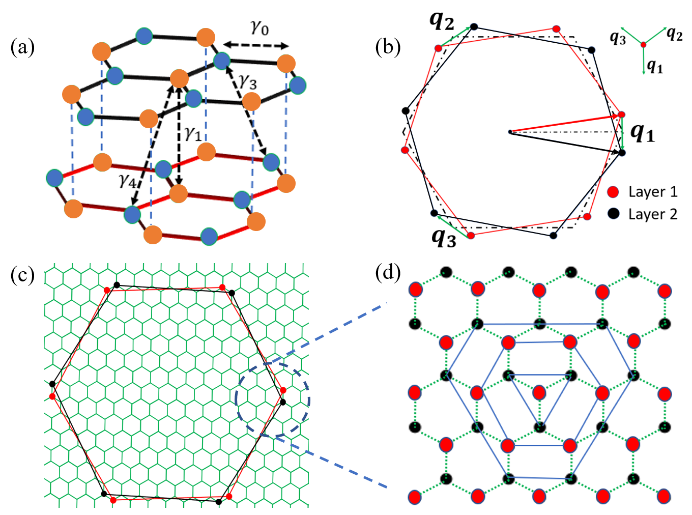
We consider the stacked tDBLG. In this case, the graphene Brillouin zone is tiled by the moirBrillouin zone (mBZ), with a reciprocal lattice vector of size , where is the reciprocal lattice vector of the BLG Brillouin zone and is the twist angle, as shown in Fig. 1(b). The two twisted layers are tunnel-coupled with tunneling between the same sublattices and the tunneling between different sublattices . For these set of parameters, used in a wide range of earlier papers Koshino 2019; Liu et al. 2020; Mohan et al. 2021, the magic angle is , which matches with experimental estimates of magic angle for tDBLG Ghosh et al. 2022. The inter-BLG tunnelings couple momentum states in one mBZ to those in nearby zones; as shown in Ref. Bistritzer and MacDonald 2011 and Fig. 1(c-d). One can limit the number of Brillouin zones used to calculate the band dispersion of the moirsystem at low twist angles Bistritzer and MacDonald 2011. We use the 5 nearest shells which lead to a dimesional continuum Hamiltonian to obtain the low energy band dispersion of tDBLG within an accuracy of .
The low energy band structure of tDBLG near the magic angle consists of a valence and a conduction band with a bandwidth . In Fig. 2(a), we plot the dispersion of the conduction and valence bands along the principal directions of the mBZ (). We clearly see that the bands overlap in energy along the line (shown by the shaded region in Fig. 2(a)) ; hence at the charge neutrality point, one would expect a compensated metal with electron and hole pockets. We would like to note that particle-hole symmetric band structures, obtained from a simplified description of BLG with only and , do not show this band overlap Mohan et al. 2021; Chebrolu et al. 2019. The presence of trigonal warping is crucial in obtaining this overlap. In Fig. 2(b), we show a 3d plot of the dispersion of the valence and the conduction band, which clearly shows that the bands do not cross each other; rather they touch each other at two anisotropic Dirac points along the line at slightly different energies, leading to the band overlap. The valence and conduction band dispersions are plotted as color plots in the full Brillouin zone in Fig 2(d) and (e). The thick lines mark the Fermi surfaces (curves) of the electron (conduction band) and hole (valence band) pockets at the CNP. We clearly see that there are three electron and three hole pockets related by symmetry. The pockets are centered around the points where the bands touch each other. We note that we have plotted the moire bands around one valley of the original BLG dispersion. The band touchings and electron-hole pockets of the other valley can be obtained by applying a rotation of to this figure.

As we move away from the CNP on the electron doped side, the size of the electron pocket increases, while the hole pocket shrinks. At an electron density , the hole pocket shrinks to a point and beyond this density, the system only has three electron pockets. Here is the density where the conduction band is fully filled (including spin and valley degeneracies). On the other hand, with hole doping, the hole pocket grows and the electron pocket shrinks, till it disappears at . Fig 2(f) plots the Fermi surfaces for the electron and hole pockets on either side of CNP at densities and to show the evolution described above. Note that the centers of the pockets do not change with density and the wave-vectors joining the centers of the nearest electron and hole pockets, , , and are clearly shown in Fig 2(f). While there are interesting evolution of the Fermi surface at higher densities, in this paper, we will focus on densities between and , where both electron and hole pockets are present.
The finite density of states at the Fermi level coming from these electron and hole pockets lead to metallic behaviour in tDBLG Cao et al. 2020; Adak et al. 2020; Burg et al. 2019; Liu et al. 2020; Shen et al. 2020 in absence of perpendicular electric field. We note that the waxing and waning of the electron and hole pockets compensate each other to keep the total density of states at the Fermi level finite and independent of the carrier density near CNP, as shown in Fig 2(c). Recently the strong magnetic field dependence of the low temperature resistance and thermopower in these systems Ghosh et al. 2022 have provided concrete evidence of the existence of these electron and hole pockets in tDBLG.
III Exciton Condensates near CNP
An important question in systems with low electronic density is: what is the fate of the system when the strong electronic interactions are taken into account? While earlier experiments in tDBLG Cao et al. 2020; Adak et al. 2020; Burg et al. 2019; Liu et al. 2020; Shen et al. 2020 showed a fairly standard metallic behaviour in absence of perpendicular electric fields (correlated states were found at finite electric fields), a recent experiment Ghosh et al. 2022 at very low temperatures () has shown a double peak structure in the resistance as a function of carrier density near CNP where both electron and hole pockets are present. These double peak structures cannot be explained by a non-interacting theory, since electrons and holes contribute additively to the electrical response, and the total density of states near CNP is almost independent of doping as seen in Fig 2(c). These are the first concrete experimental signatures that electronic correlations play an important role in tDBLG near the CNP.
In systems with electron and hole states at the Fermi level, the Coulomb attraction between the oppositely charged electrons and holes often leads to the formation of charge neutral electron-hole pairs called excitons. Formation of exciton states are commonly seen in semiconductor systems Halperin and Rice 1968; Khveshchenko and Leal 2004, as well as Van der Waals heterostructures Zhang et al.; Chen et al.. Coherent condensation of these particle-hole pairs, leading to superfluidity of charge neutral objects, have been predicted and demonstrated in bilayer quantum Hall systems Eisenstein 2014; Wang et al. 2019; Kogar et al. 2017; Li et al. 2017 as well as bilayer graphene Ju et al. 2017. The electron-hole pockets in tDBLG, which are separated by a small momentum , are ideal candidates for the formation of excitonic condensates with finite momentum (indirect excitons). We will now explore this possibility within mean field theory.

We consider the two-band Hamiltonian
| (1) | |||||
where denotes the electron annihilation operator in the conduction (valence) band, is a composite spin and valley index and is the conduction and valence band dispersions shown in the previous section. Here is the screened Coulomb interaction between the conduction and valence band electrons. We note that we have neglected interaction between electrons in the same band, since our primary focus is on understanding the formation of interband excitons. We have also assumed that the large momentum connecting the two valleys of BLG makes it unfavourable for Coulomb interaction to scatter electrons from one valley to the other. Note that although excitons are often understood as pairing of electrons and holes, where the hole can be obtained by a particle-hole transformation on the valence band, i.e. , we prefer to work with electron coordinates in both bands. The size of the small Fermi pockets as well as the momentum separating the center of the electron and hole pockets are . We assume that does not change rapidly over this scale and can be approximated by a constant value for our calculation. For our calculations, we will use where . We will later try to constrain its value both from theoretical and experimental estimates.
From Fig. 2(f), we see that there are three electron and hole pockets in the mBZ, and three wave-vectors connecting them. We will consider a mean-field description of finite momentum interband excitonic condensate, which has an equal amplitude at each of the momenta , i.e. (See Fig. 3(a) for a schematic of finite momentum exciton). We note that formation of finite momentum excitonic condensates in this system is equivalent to the appearance of a charge density wave (CDW) order in the system. Since , our ansatz of equal condensates for all momenta ensure that there is no underlying valley current in the ground state of the system. It also ensures that the symmetry of each valley remains unbroken in the system. Note that , if the valley is flipped, and the net current summed over valleys would have been zero even for an ansatz with unequal condensates. With this ansatz, using the basis , we obtain the mean field Hamiltonian,
| (2) |
where
| (3) |
Here and vectors are generated by rotating the vector by and respectively. The quasiparticle excitation spectrum of the mean field theory is
| (4) |
The self-consistency equations, which determine the order parameter and the chemical potential , are given by
| (5) |
where is the Fermi function. In Fig. 3(b) we plot the self-consistent at as a function of the carrier density for a system with . The order parameter shows a maxima around the CNP () and decreases on either side of CNP, finally vanishing through a sharp jump at the boundaries where the electron-hole pockets cease to exist simultaneously. The electron and hole pockets are matched in size (albeit shifted in momentum) at the CNP. As we move away, the electron(hole) pocket grows while the hole (electron) pocket shrinks. This mismatch of the Fermi pockets leads to a weakening of the order parameter at finite carrier densities. The temperature dependence of the order parameter at three different densities are shown in Fig. 3(c). From the vanishing of the order parameter, one can obtain the mean-field of the system, which is plotted in Fig. 3(c) inset as a function of carrier density. We see that is very weakly dependent on carrier density and hovers around for our chosen set of parameters. Our estimate is in the same ballpark as the experimentally obtained Ghosh et al. 2022, where the resistance peaks disappear. We would like to note that this mean-field estimate is an upper bound for the real , which will be further degraded by fluctuations and disorder. In Fig. 3(d), we have shown the dependence of and at CNP. The magenta horizontal line is the experimentally observed Ghosh et al. 2022. The black horizontal line corresponds to the maximum value of for which the system remains metallic (see discussion in Sec. IV for details). These two lines thus provide lower and upper bounds on ( and respectively) to be used in the calculation. We have used in the middle of this range.

IV Exciton condensates and Electronic Structure
The occurrence of excitonic condensates in materials Khveshchenko and Leal 2004; Jia et al. 2021; Halperin and Rice 1968; Zhang et al. often lead to the underlying Fermi surface being gapped out, leading to an excitonic insulator. This is inevitably the case when the condensate is formed with net momentum, as is the case in quantum Hall bilayers and bilayer graphene Eisenstein 2014; Wang et al. 2019; Kogar et al. 2017; Li et al. 2017; Ju et al. 2017. However, the shift between the center of the electron and hole pockets in tDBLG near CNP naturally leads to excitonic condensates with finite momenta. This leads to the possibility of having either metallic or insulating behaviour depending on the magnitude of the excitonic order in the system and the resulting quasiparticle spectrum . Note that the original 2-band system is mapped to a band system in the presence of excitonic order.
A simple measure of metallicity of the system is the density of states at the Fermi level, . For metals we expect to be finite, while it should go to for insulators. We now consider how behaves with carrier density for different values of . These values are not obtained from a self-consistent solution of the gap equation; rather our intention is to vary and understand the range of values for which we can recover the metallic behaviour seen in the experiments. For each , we solve the number equation to obtain the Fermi level for the excitonic quasiparticles. In Fig. 4(a), we plot as a function of the order parameter at CNP. Here is the density of states at the Fermi level of the non-interacting system at CNP. For the system is insulating in nature and below that it’s a metal. Since the experimental data Ghosh et al. 2022 clearly shows metallic behaviour at low temperatures for all densities near CNP, this provides an upper bound for the possible values of . Within the mean field theory, this in turn provides an upper bound on the interaction strength . For , we obtain . In this work, we use a value of which is consistent with earlier work Cea and Guinea 2020.

In recent experiments, resistance of tDBLG at low temperatures have shown a distinct two-peak structure as a function of carrier density near CNP. This is seen in the region where electron and hole pockets are simultaneously present. A representative experimental data is shown in Fig. 4(b). We will use the inverse of the density of states at the Fermi level as a proxy for the resistivity of the system. This assumes that Fermi velocity is not sharply anisotropic in the density range considered, which is valid for tDBLG near CNP with its small electron and hole pockets. In Fig. 4(c), we plot as a function of carrier density for a system with indirect excitonic condensate (). We clearly see the presence of two peaks, as seen in the experiments. For comparison, we have also plotted for the non-interacting system, which does not show any structure in the relevant density range. This shows that the presence of excitonic condensate can explain the double peak structure seen in experiments. In Fig. 4(d) we plot with carrier density for different interaction strengths and see that the two-peak feature is lost for . This is close to the lower bound obtained from experimental discussed in the earlier section.
In order to theoretically understand the origin of the two peaks, we look at the dispersion of the bands in presence of the excitonic condensate (detail band dispersion of all 6 bands are plotted in Appendix. B). In Fig. 4(e-h), we plot the Fermi surfaces of the quasiparticles (with spectrum ) in the mBZ for four different carrier densities, . At CNP ( Fig. 4(e) ), we find that both and bands pass through the Fermi level, and hence give rise to their respective Fermi surfaces (shown by green and pink lines respectively). This leads to the finite density of states at Fermi energy and hence to metallic behaviour in the system. As we move away from the CNP on the electron doped side, the Fermi surfaces corresponding to reduces, while that of bands increases in size ( Fig. 4(e)-(h)). This leads to a reduction in the density of states at the Fermi level and hence to an increase in resistivity till the Fermi surface vanishes at ( Fig. 4(g) ), which corresponds to the peak in the inverse density of states. Beyond this point, we see additional Fermi surfaces as the chemical potential enter one of the bands which was gapped at CNP. This leads to a large increase in the density of states at the Fermi level and consequently a sharp decrease in the resistivity, explaining the peak seen in the resistivity for . A similar argument, with the roles of and reversed, explains the peak for . We would like to note that the transport features are expected to be more smeared than single particle features due to the presence of inhomogeneities in the system. This is consistent with the experiments, which see relatively smoother features compared to the theoretical estimates.
V Temperature Dependence of Resistivity and Non-Fermi Liquid Behaviour
An intriguing signature of strong electronic correlations is seen in recent experiments Ghosh et al. 2022 on the temperature dependence of resistance of tDBLG near the charge neutrality point. The resistance shows a sublinear ( with ) behaviour up to , and an almost linear behaviour above that temperature(Fig. 5(b)). In contrast, the temperature dependence of resistance at larger electron (hole) densities, () and (), are superlinear and can be fitted to the standard quadratic Fermi liquid scaling, with , expected for a 2d system with small Fermi pockets, both from electron-electron and electron-phonon scattering. This is shown in Fig 5(a) and (c).
This novel sublinear behaviour cannot be explained within a Fermi liquid paradigm of perturbative effects of electronic interactions around a free Fermi gas. Electron-electron interactions lead to a dependence of the resistivity. In 2 dimensions, the density of states of longitudinal phonons . This leads to dependence of resistivity when small angle scattering dominates at low temperatures and behaviour of resistivity when scattering at all angles contributes. For compensated semi-metals like tDBLG, with small Fermi surfaces, one would expect the resistivity . At higher temperatures (beyond the Bloch Gruneissen temperature), the scattering from classical phonons would lead to a linear dependence of resistivity Wu et al. 2019. None of these mechanisms can explain a sublinear temperature dependence of resistivity, as is seen in the experiments.
In this section, we will show that a tDBLG system near CNP, which is at the precipice of a quantum criticality towards the formation of an excitonic condensate, will show a sublinear temperature dependence of resistance. At criticality, the low energy gapless fluctuations of the excitonic (CDW) order parameter would be strongly Landau damped due to the presence of the electronic states of the metal around the Fermi surfaces. The scattering between electrons and the Landau damped fluctuations lead to a non-analytic low energy decay rate for the single particle electronic excitations, resulting in non-Fermi liquid behaviour. For compensated semimetals like tDBLG, with small Fermi surfaces, the transport scattering rate and the quasiparticle scattering rate has the same energy dependence. This non-analytic frequency dependence of the scattering rate leads to the sublinear temperature dependence of resistivity in this system. We note that this mechanism is an alternate to theories of Planckian metal Patel and Sachdev 2019, which predicts linear temperature dependence of resistivity all the way down to .
The fluctuations of the order parameter, are governed by an action,
| (6) |
where is the (interacting) inter-band polarizability of the system. When driven to the critical point, ; i.e. the gap vanishes (this can be seen within a simple RPA like theory), and generically we would have
| (7) |
where , and are constants denoting the speed of the fluctuation waves and the scale of damping. The singular damping is a consequence of the presence of low energy fermions, and derives from the imaginary part of the non-interacting inter-band polarizability.
The non-interacting interband polarizability of the system is given by
| (8) |
where is the Fermi function and is the Bloch wavefunction of the corresponding band in the mBZ. To see the Landau damping, in Fig. 6(a), we plot the imaginary part of as a function of for several values of along the direction. Note that is along direction, so we will be crossing the exciton wave-vector in the process. At low , the plots are linear and we extract a slope from this linear part of the graph. The slope is plotted as a function of in Fig. 6(b). The slope diverges at , showing the singular nature of the Landau damping. We have checked by taking momentum cuts along other directions passing through , that the divergence of the slope happens whenever we approach along any direction, i.e. there is no difference in the scaling between directions along and perpendicular to the exciton/CDW wave-vector (see Appendix. A for details).
We can understand this further by constructing a simple model for
the valence and conduction band. The electron pocket of the conduction band is modeled by a
Dirac dispersion centered around , i.e. ,
while the hole pocket in the valence band is modeled by an inverted Dirac dispersion
centered around , i.e. in Fig. 6(c). Here is the energy difference between the
Dirac points. At CNP, the chemical potential sits at
giving a Fermi wave vector for electrons and holes. Usually, the orthogonality of the band wavefunctions as plays an important role in determining the low behaviour of in graphene. However, here we are interested in near where orthogonality considerations do not play a role. The band overlaps do not change the scaling of
various terms (although they can change the value of the coefficients like
etc.). Hence we ignore band overlaps in our calculation of . In this case, the polarization function can be
calculated exactly and the detailed formulae are given in
Appendix A. Near , the imaginary part of has the
following form:
| (9) | |||||
Thus both the numerical calculation on the full model and the analytic calculation with the simple model shows the presence of the singular Landau damping around .

The Landau damped fluctuations have an energy momentum relation , leading to a density of states . The scattering of electrons by these fluctuations lead to a single particle scattering rate
| (10) | |||||
| (11) |
where is a cutoff below which the long wave-length description mentioned above holds with the condition . The damping rate is larger than the energy of excitations leading to non-Fermi liquid behaviour. Since the Fermi pockets in tDBLG near CNP are small, scattering at all angles contribute to transport and hence the transport scattering rate . This is the origin of the dependence of resistance in the system. Thus the sublinear temperature dependence is a reflection of an underlying non-Fermi liquid state in a quantum critical metal.
Starting with the work of Hertz and Millis, Hertz 1976; Millis 1993, non-Fermi liquid behaviour of itinerant quantum critical systems have been studied in the context of high temperature superconductivity Polchinski 1994; Senthil et al. 2004a; Sachdev 2000, for the antiferromagnetic metal Sachdev 2012; Vekhter and Chubukov 2004; Liu et al. and for the nematic transition in metals Metlitski and Sachdev 2010a; Klein et al. 2020 using sophisticated renormalization group techniques. The general conclusion is that the imaginary part of the electron self energy when the order parameter is at wave vector Metlitski and Sachdev 2010a (as in nematic transition), while we get a dependence for a finite wave-vector order like spin density waves Metlitski and Sachdev 2010b. We note that in our case the finite wave-vector relates the center of the electron pocket to the center of the hole pocket, so the electron and hole Fermi surfaces lie on top of each other when shifted by this wave vector. Thus, although the CDW is formed at finite wave vector, our itinerant quantum criticality is similar to the nematic case with effective and we recover the scaling.
In the experiments, it is seen that the resistivity shows a linear temperature dependence above . We note that the Fermi temperature corresponding to the e-h pockets is and one would expect quantum behaviours to vanish beyond this temperature. For a 2-dimensional system with small Fermi surfaces, a more relevant scale would be the effective “Bloch Gruneissen” temperature of these critical fluctuations, i.e. their energy for . While this requires interaction renormalized estimates of and , which are beyond the scope of this paper, one would expect this temperature to be lower than . If we assume that beyond , these fluctuations are classical, we can obtain the linear temperature dependence of resistivity in this regime.
As we move away from the CNP on either side, the mismatch between the electron and hole Fermi surfaces increases, and the Landau damping would be shifted to finite , where is the mismatch of the Fermi wave vectors of the electron and hole pockets. In this case, the low temperature behaviour of resistivity would deviate from the scaling. Assuming the scaling of the Landau damping is cut-off on the scale of , i.e. it scales as , one would get a linear dependence of the resistivity. However, this exponent would be strongly influenced by disorder and Fermi surface anisotropies. In general, one would expect the exponent to increase as one goes away from CNP. Once the simultaneous presence of electron and hole pockets vanish at larger doping, one gets back the standard scaling of the Fermi liquid theory.
VI Conclusion
Strong electronic interactions determine the plethora of symmetry broken phases in magic angle tBLG and tTLG. In contrast, tDBLG is usually thought of as a plain vanilla metal in the absense of electric/magnetic fields. The metallicity of magic angle tDBLG near CNP comes from the overlap of flat conduction and valence bands which creates small electron and hole pockets at the Fermi surface.
In this paper, we have considered the possible effects of Coulomb interaction on these small e-h pockets in the compensated semi-metal near CNP. We show that the interactions lead to the formation of indirect excitons (i.e. particle-hole pairs with finite momenta). The condensation of such pairs lead to the formation of CDW states. We show that for a reasonable range of interaction parameters, this ordered state has reorganised Fermi pockets and hence metallic behaviour is expected. However, the density of electronic states is strongly renormalised in the process. The inverse density of states at Fermi level shows peaks at finite doping on either side of CNP. This can explain the peaks in the resistance as a function of density seen in recent low temperature experiments Ghosh et al. 2022. We further show that the Landau damped critical fluctuations of the excitonic order can give rise to non-Fermi liquid behaviour of the electrons with a scattering rate, . For systems like tDBLG, with small Fermi pockets, this can give rise to sub-linear resistance seen in recent experiments Ghosh et al. 2022.
Our theoretical predictions thus strongly indicate that effect of excitonic/CDW order and its fluctuations have already been observed through the non-Fermi liquid temperature dependence of resistivity. A hallmark of CDW insulators is the current produced by sliding mode when the order is depinned by finite energy probes(non-linear/AC conductivity). However, in a metallic system like tDBLG, these contributions would be masked by the usual single particle contributions. We believe the fluctuations of the finite particle-hole condensate should give additional contributions to current noise but we leave this calculation for a future manuscript.
VII Acknowledgement
R.S. would like to thank Mohit Randeria for useful discussions. UG and RS acknowledge computational facilities at the Department of Theoretical Physics, TIFR Mumbai. R.S. acknowledges support of the Department of Atomic Energy, Government of India, under Project Identification No. RTI 4002. UG would like to thank Md. Mursalin Islam for useful discussions related to computational part of the project.
References
- Bistritzer and MacDonald (2011) R. Bistritzer and A. H. MacDonald, Proceedings of the National Academy of Sciences 108, 12233 (2011).
- Lopes dos Santos et al. (2012) J. M. B. Lopes dos Santos, N. M. R. Peres, and A. H. Castro Neto, Physical Review B 86, 155449 (2012).
- Koshino et al. (2018) M. Koshino, N. F. Q. Yuan, T. Koretsune, M. Ochi, K. Kuroki, and L. Fu, Phys. Rev. X 8, 031087 (2018).
- Lopes dos Santos et al. (2007) J. M. B. Lopes dos Santos, N. M. R. Peres, and A. H. Castro Neto, Physical Review Letters 99, 256802 (2007), arXiv:0704.2128 .
- Bernevig et al. (2021) B. A. Bernevig, Z.-D. Song, N. Regnault, and B. Lian, Physical Review B 103, 205411 (2021).
- Carr et al. (2017) S. Carr, D. Massatt, S. Fang, P. Cazeaux, M. Luskin, and E. Kaxiras, Phys. Rev. B 95, 075420 (2017).
- Tarnopolsky et al. (2019) G. Tarnopolsky, A. J. Kruchkov, and A. Vishwanath, Physical Review Letters 122, 106405 (2019), arXiv:1808.05250 .
- Zou et al. (2018) L. Zou, H. C. Po, A. Vishwanath, and T. Senthil, Phys. Rev. B 98, 085435 (2018).
- Chebrolu et al. (2019) N. R. Chebrolu, B. L. Chittari, and J. Jung, Phys. Rev. B 99, 235417 (2019).
- Mohan et al. (2021) P. Mohan, U. Ghorai, and R. Sensarma, Physical Review B 103, 155149 (2021).
- Cao et al. (2018a) Y. Cao, V. Fatemi, A. Demir, S. Fang, S. L. Tomarken, J. Y. Luo, J. D. Sanchez-Yamagishi, K. Watanabe, T. Taniguchi, E. Kaxiras, R. C. Ashoori, and P. Jarillo-Herrero, Nature. 556, 80 (2018a).
- Cao et al. (2018b) Y. Cao, V. Fatemi, S. Fang, K. Watanabe, T. Taniguchi, E. Kaxiras, and Jarillo-Herrero, Nature. 556, 43–50 (2018b).
- Yankowitz et al. (2019) M. Yankowitz, S. Chen, H. Polshyn, Y. Zhang, K. Watanabe, T. Taniguchi, D. Graf, A. F. Young, and C. R. Dean, Science 363, 1059 (2019).
- Park et al. (2021a) J. M. Park, Y. Cao, K. Watanabe, T. Taniguchi, and P. Jarillo-Herrero, Nature 590 (2021a), 10.1038/s41586-021-03192-0.
- Hao et al. (2021) Z. Hao, A. M. Zimmerman, P. Ledwith, E. Khalaf, D. H. Najafabadi, K. Watanabe, T. Taniguchi, A. Vishwanath, and P. Kim, Science 371, 1133 (2021).
- Park et al. (2021b) J. M. Park, Y. Cao, L. Xia, S. Sun, K. Watanabe, T. Taniguchi, and P. Jarillo-Herrero, “Magic-angle multilayer graphene: A robust family of moiré superconductors,” (2021b).
- Cao et al. (2020) Y. Cao, D. Rodan-Legrain, O. Rubies-Bigorda, J. M. Park, K. Watanabe, T. Taniguchi, and P. Jarillo-Herrero, Nature 583, 215–220 (2020).
- Burg et al. (2019) G. W. Burg, J. Zhu, T. Taniguchi, K. Watanabe, A. H. MacDonald, and E. Tutuc, Phys. Rev. Lett. 123, 197702 (2019).
- Adak et al. (2020) P. C. Adak, S. Sinha, U. Ghorai, L. D. V. Sangani, K. Watanabe, T. Taniguchi, R. Sensarma, and M. M. Deshmukh, Phys. Rev. B 101, 125428 (2020).
- Mishchenko et al. (2014) A. Mishchenko, J. S. Tu, Y. Cao, R. V. Gorbachev, J. R. Wallbank, M. T. Greenaway, V. E. Morozov, S. V. Morozov, M. J. Zhu, S. L. Wong, F. Withers, C. R. Woods, Y.-J. Kim, K. Watanabe, T. Taniguchi, E. E. Vdovin, O. Makarovsky, T. M. Fromhold, V. I. Fal’ko, A. K. Geim, L. Eaves, and K. S. Novoselov, (2014), 10.1038/NNANO.2014.187.
- Zhang et al. (2020) Z. Zhang, Y. Wang, K. Watanabe, T. Taniguchi, K. Ueno, E. Tutuc, and B. J. LeRoy, NaTURE PhYsics — 16, 1093 (2020).
- (22) L. Wang, E.-M. Shih, A. Ghiotto, L. Xian, D. A. Rhodes, C. Tan, M. Claassen, D. M. Kennes, Y. Bai, B. Kim, K. Watanabe, T. Taniguchi, X. Zhu, J. Hone, A. Rubio, A. N. Pasupathy, and C. R. Dean, 10.1038/s41563-020-0708-6.
- Lu et al. (2019) X. Lu, P. Stepanov, W. Yang, M. Xie, M. A. Aamir, I. Das, C. Urgell, K. Watanabe, T. Taniguchi, G. Zhang, A. Bachtold, A. H. MacDonald, and D. K. Efetov, Nature 574, 653 (2019), arXiv:1903.06513 .
- Liu et al. (2020) X. Liu, Z. Hao, E. Khalaf, J. Y. Lee, Y. Ronen, H. Yoo, D. H. Najafabadi, K. Watanabe, T. Taniguchi, A. Vishwanath, and P. Kim, Nature. 583, 221 (2020).
- Nuckolls et al. (2020) K. P. Nuckolls, M. Oh, D. Wong, B. Lian, K. Watanabe, T. Taniguchi, B. A. Bernevig, and A. Yazdani, Nature — 588, 610 (2020).
- Sharpe et al. (2019) A. L. Sharpe, E. J. Fox, A. W. Barnard, J. Finney, K. Watanabe, T. Taniguchi, M. A. Kastner, and D. Goldhaber-Gordon, Science 365, 605 (2019).
- Oh et al. (2021) M. Oh, K. P. Nuckolls, D. Wong, R. L. Lee, X. Liu, K. Watanabe, T. Taniguchi, and A. Yazdani, 240 — Nature — 600 (2021), 10.1038/s41586-021-04121-x.
- (28) Y. Saito, J. Ge, K. Watanabe, T. Taniguchi, and A. F. Young, 10.1038/s41567-020-0928-3.
- Cao et al. (2021) Y. Cao, J. M. Park, K. Watanabe, T. Taniguchi, and P. Jarillo-Herrero, Nature 595, 526 (2021).
- Chen et al. (2019) G. Chen, A. L. Sharpe, P. Gallagher, I. T. Rosen, E. J. Fox, L. Jiang, B. Lyu, H. Li, K. Watanabe, T. Taniguchi, J. Jung, Z. Shi, D. Goldhaber-Gordon, Y. Zhang, and F. Wang, Nature 572, 215 (2019).
- Burg et al. (2020) G. W. Burg, B. Lian, T. Taniguchi, K. Watanabe, B. A. Bernevig, and E. Tutuc, (2020), arXiv:2006.14000 .
- Koshino (2019) M. Koshino, Phys. Rev. B 99, 235406 (2019).
- Ghosh et al. (2022) A. Ghosh, S. Chakraborty, U. Ghorai, A. K. Paul, K. Watanabe, T. Taniguchi, R. Sensarma, and A. Das, (2022), 10.48550/ARXIV.2211.02654.
- Metlitski and Sachdev (2010a) M. A. Metlitski and S. Sachdev, Physical Review B 82, 075127 (2010a), arXiv:1001.1153 .
- Hertz (1976) J. A. Hertz, Phys. Rev. B 14, 1165 (1976).
- Millis (1993) A. J. Millis, Phys. Rev. B 48, 7183 (1993).
- Lee et al. (2013) J. Lee, P. Strack, and S. Sachdev, Phys. Rev. B 87, 045104 (2013).
- Vekhter and Chubukov (2004) I. Vekhter and A. Chubukov, Physical Review Letters 93, 016405 (2004), arXiv:0401375 [cond-mat] .
- Senthil et al. (2004a) T. Senthil, A. Vishwanath, L. Balents, S. Sachdev, and M. P. A. Fisher, Science 303, 1490 (2004a), arXiv:0311326 [cond-mat] .
- Polchinski (1994) J. Polchinski, Nuclear Physics B 422, 617 (1994).
- Senthil et al. (2004b) T. Senthil, M. Vojta, and S. Sachdev, Physical Review B 69 (2004b), 10.1103/physrevb.69.035111.
- Metlitski and Sachdev (2010b) M. A. Metlitski and S. Sachdev, Phys. Rev. B 82, 075128 (2010b).
- Christos et al. (2022) M. Christos, S. Sachdev, and M. S. Scheurer, Physical Review X 12 (2022), 10.1103/physrevx.12.021018.
- Li et al. (2019) X. Li, F. Wu, and A. H. MacDonald, “Electronic structure of single-twist trilayer graphene,” (2019).
- Shen et al. (2020) C. Shen, Y. Chu, Q. Wu, N. Li, S. Wang, Y. Zhao, J. Tang, J. Liu, J. Tian, K. Watanabe, T. Taniguchi, R. Yang, Z. Y. Meng, D. Shi, O. V. Yazyev, and G. Zhang, Nat. Phys. 16, 520–525 (2020).
- McCann and Koshino (2013) E. McCann and M. Koshino, Reports on Progress in Physics 76, 056503 (2013).
- Lemonik et al. (2010) Y. Lemonik, I. L. Aleiner, C. Toke, and V. I. Fal’ko, Phys. Rev. B 82, 201408 (2010).
- Varlet et al. (2014) A. Varlet, D. Bischoff, P. Simonet, K. Watanabe, T. Taniguchi, T. Ihn, K. Ensslin, M. Mucha-Kruczyński, and V. I. Fal’ko, Phys. Rev. Lett. 113, 116602 (2014).
- Halperin and Rice (1968) B. Halperin and T. Rice, Solid State Physics, 21, 115 (1968).
- Khveshchenko and Leal (2004) D. Khveshchenko and H. Leal, Nuclear Physics B 687, 323 (2004).
- (51) Z. Zhang, E. C. Regan, D. Wang, W. Zhao, S. Wang, M. Sayyad, K. Yumigeta, K. Watanabe, T. Taniguchi, S. Tongay, M. Crommie, A. Zettl, M. P. Zaletel, and F. Wang, 10.1038/s41567-022-01702-z.
- (52) D. Chen, Z. Lian, X. Huang, Y. Su, M. Rashetnia, L. Ma, L. Yan, M. Blei, L. Xiang, T. Taniguchi, K. Watanabe, S. Tongay, D. Smirnov, Z. Wang, C. Zhang, Y.-T. Cui, and S.-F. Shi, 10.1038/s41567-022-01703-y.
- Eisenstein (2014) J. Eisenstein, Annual Review of Condensed Matter Physics 5, 159 (2014), https://doi.org/10.1146/annurev-conmatphys-031113-133832 .
- Wang et al. (2019) Z. Wang, D. A. Rhodes, K. Watanabe, T. Taniguchi, J. C. Hone, J. Shan, and K. F. Mak, Nature 574, 76 (2019).
- Kogar et al. (2017) A. Kogar, M. S. Rak, S. Vig, A. A. Husain, F. Flicker, Y. I. Joe, L. Venema, G. J. MacDougall, T. C. Chiang, E. Fradkin, J. van Wezel, and P. Abbamonte, Science 358, 1314 (2017), https://www.science.org/doi/pdf/10.1126/science.aam6432 .
- Li et al. (2017) J. I. A. Li, T. Taniguchi, K. Watanabe, J. Hone, and C. R. Dean, Nature Physics 13, 751 (2017).
- Ju et al. (2017) L. Ju, L. Wang, T. Cao, T. Taniguchi, K. Watanabe, S. G. Louie, F. Rana, J. Park, J. Hone, F. Wang, and P. L. McEuen, Science 358, 907 (2017).
- Jia et al. (2021) Y. Jia, P. Wang, C.-L. Chiu, Z. Song, G. Yu, B. Jäck, S. Lei, S. Klemenz, F. A. Cevallos, M. Onyszczak, N. Fishchenko, X. Liu, G. Farahi, F. Xie, Y. Xu, K. Watanabe, T. Taniguchi, B. A. Bernevig, R. J. Cava, L. M. Schoop, A. Yazdani, and S. Wu, Nature Physics 18, 87 (2021).
- Cea and Guinea (2020) T. Cea and F. Guinea, Physical Review B 102, 045107 (2020).
- Wu et al. (2019) F. Wu, E. Hwang, and S. Das Sarma, Phys. Rev. B 99, 165112 (2019).
- Patel and Sachdev (2019) A. A. Patel and S. Sachdev, Phys. Rev. Lett. 123, 066601 (2019).
- Sachdev (2000) S. Sachdev, Science 288, 475 (2000), arXiv:0009456 [cond-mat] .
- Sachdev (2012) S. Sachdev, in Modern Theories of Many-Particle Systems in Condensed Matter Physics (Springer Berlin Heidelberg, 2012) pp. 1–51.
- (64) C. Liu, V. F. Humbert, T. M. Bretz-Sullivan, G. Wang, D. Hong, F. Wrobel, J. Zhang, J. D. Hoffman, J. E. Pearson, J. S. Jiang, C. Chang, A. Suslov, N. Mason, M. Norman, and A. Bhattacharya, 10.1038/s41467-020-15143-w.
- Klein et al. (2020) A. Klein, A. V. Chubukov, Y. Schattner, and E. Berg, Physical Review X 10, 31053 (2020), arXiv:2003.09431 .
Appendix
Appendix A Interband Polarizability and Landau damping
We are interested in the low energy dispersion of valence and conduction bands in tDBLG, especially the modes which constitute the electron ad hole pockets near the CNP. For these modes, the energy dispersion can be approximated as two Dirac cones separated in momentum and energy as shown in Fig. 6(c). We use the hole band of the Dirac cone inverted around higher Dirac point and the electron band around lower Dirac point as,
| (12) |
Here, is the energy dispersion of conduction(valence) band, is the chemical potential at CNP, denotes the Fermi velocity of the effective Dirac points and the momentum separation wavevector between two Dirac cones is given by . Also one can note that exciton order parameter , so its fluctuations, are related to the non-interacting interband polarizability,
| (13) |
Where the total polarizability . Usually the orthogonality of the band wavefunctions as plays an important role in determining the low behaviour of in Graphene. However, here we are interested in near where orthogonality considerations do not play a role. The band overlaps do not change the scaling of various terms. Hence we can drop the term from Eq. 13 and write it as,
| (14) |
where . Now using dimensionless parameters, , the Eq. 14 can be rewritten as,
Here is the azimuthal angle between and . Here is an ultraviolet cut-off. We note that the Landau damping we calculate is a low energy property, which is independent of . We are interested in the imaginary part of the polrizability, , which then becomes,
Here . This azimuthal integral can be done analytically to get,
which can also be written as,
| (15) |
where, . We will work with and so that, and, . In this case, . Now depending on the value of we can have different regions in the phase space where the integrals take qualitatively different forms,
Case-(i):
and ,
or, and ,
| (16) | |||||
Case-(ii):
and ,
| (17) | |||||
Therefore we analytically show the Landau damping factor() arising from imaginary part of the interband polarizability function assuming two simple Dirac bands separated from each other in energy and momentum space. One can easily see that will give the same contribution. Collecting all these,
| (18) | |||||
| (19) |

As shown in the main text, the numerical evaluation of using the actual tDBLG dispersion and wavefunctions also give rise to similar singular damping. In the main text, we looked at as a function of . Here in Fig. 7 (b), we additionally plot the slope along a cut in which passes through and moves along [0,1]() and [1,1]() directions (the directions are schematically shown in Fig. 7(a)). We see that the slope diverges at irrespective of the direction in which it is approached. Thus the Landau damping has only small anisotropies riding on an isotropic background, even though the Fermi velocities at the Dirac points are anisotropic. This isotropy is important for scaling arguments used to explain resistivity.
Appendix B Band renormalization due to exciton formation
In the main text, we had shown that the presence of excitonic order leads to formation of 6 minibands out of the original tDBLG dispersion. Here, we present the detailed dispersion of these 6 bands and how they change with density around CNP in Fig. 8-10. In Fig. 8, we plot the dispersion of the 6 bands (3 conduction bands in top row and 3 valence bands in bottom row) at CNP as a color plot. The electron and hole Fermi surfaces are shown as solid lines. Note that the dispersion of the bands are not symmetric for individual ’s. The e-h pocket that is coupled by the excitonic order is gapped out. Fig. 9 plots the same dispersion at . One can see that the electron pockets have grown while the hole pockets have shrunk to zero. Finally, the Fig. 10 plots the dispersion at . The hole pockets from the valence band have vanished and electron pockets are still present. But additional electron pockets appear in the conduction band. The extra density of states from these new pockets lead to a suppression of resistivity giving rise to the two-peak structure in the resitivity vs density data Ghosh et al. 2022.


