Scalable and self-correcting photonic computation using balanced photonic binary tree cascadesPreprint: APS/123-QED
Abstract
Programmable unitary photonic networks that interfere hundreds of modes are emerging as a key technology in energy-efficient sensing, machine learning, cryptography, and linear optical quantum computing applications. In this work, we establish a theoretical framework to quantify error tolerance and scalability in a more general class of “binary tree cascade” programmable photonic networks that accept up to tens of thousands of discrete input modes . To justify this scalability claim, we derive error tolerance and configuration time that scale with for balanced trees versus in unbalanced trees, despite the same number of total components. Specifically, we use second-order perturbation theory to compute phase sensitivity in each waveguide of balanced and unbalanced networks, and we compute the statistics of the sensitivity given random input vectors. We also evaluate such networks after they self-correct, or self-configure, themselves for errors in the circuit due to fabrication error and environmental drift. Our findings have important implications for scaling photonic circuits to much larger circuit sizes; this scaling is particularly critical for applications such as principal component analysis and fast Fourier transforms, which are important algorithms for machine learning and signal processing.
I Introduction
Reconfigurable photonic networks or meshes of interferometers are capable of transforming optical modes for quantum computation, energy-efficient deep learning, mode unscrambling, sensing, and beamforming Bogaerts et al. 2020. In such applications, a set of waveguide modes containing data or bits are fed into a mesh network of reconfigurable photonic interferometers and phase shifters whose output represents a matrix multiplication, where the matrix is represented by the transmission matrix of the optical device in the basis of waveguide modes. The ability to perform matrix multiplication in an ultra-fast and energy efficient manner is an attractive property of reconfigurable photonic circuits, which significantly broadens the application space for such devices. This approach also promises a new way of performing self-aligning optics with no moving parts which has applications in high-speed sensing and optical phased arrays Miller 2013a; Miller 2020. However, a key problem with this architecture is the presence of systematic errors that build up over various stages of the photonic circuit, requiring the definition of a theory of sensitivity.
In this paper, we discuss a common class of reconfigurable photonic networks that contain a network or “mesh” of Mach-Zehnder interferometers (MZIs), which can be used to progressively interfere pairs of waveguide modes. These modes may be generated in a number of ways; machine learning and photonic computing might use integrated modulators on a photonic chip operated ideally at sub-nanosecond time scales using electro-optic modulation Wang et al. 2018a and using a laser source tuned to a wavelength of interest (e.g. 1550 nm). Alternatively, these modes can arrive directly from free space as outputs of photonic sensors. This idea is still relatively unexplored but is a major focus of recent work Miller 2020 showing that multimode fields can be analyzed directly by training self-configurable networks of interferometers arranged in a “binary tree” configuration. Such modes convert a continuous free space intensity pattern into a discrete sequence of complex numbers with amplitude and phase characterizing light in the fundamental mode of a single-mode waveguide. Pairs of modes can be constructively and/or destructively interfered sequentially as they propagate through feedforward meshes of interferometers. This can be achieved programmatically by adjusting active phase shifting elements within MZIs placed in the photonic circuit. Such phase shifting elements, the pathway for programming analog matrix multiplication and signal processing in photonics, can operate by modulating the effective mode index thermally Harris et al. 2014, electromechanically Errando-Herranz et al. 2020; Edinger et al. 2020, using phase change co-integration Wuttig et al. 2017, or electrooptically Wang et al. 2018b.
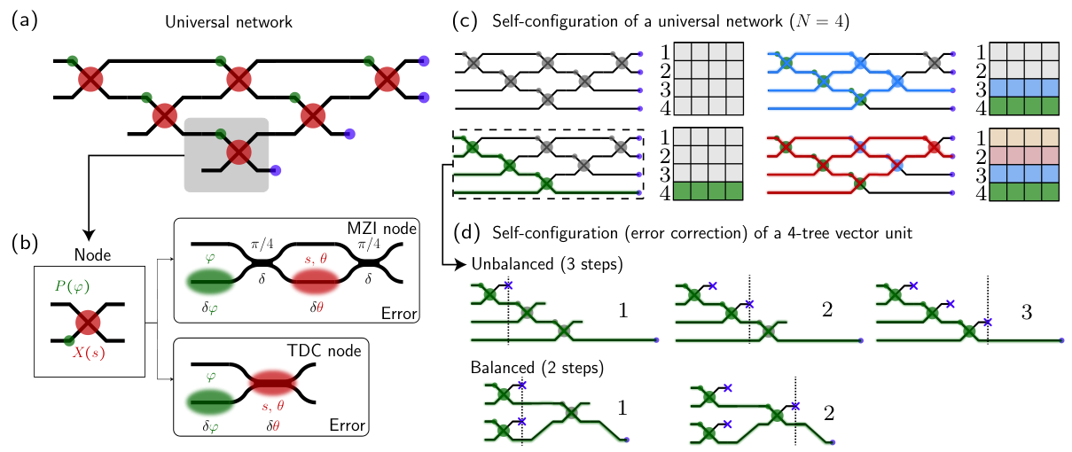
As shown in Fig. 1(a), a triangular network of MZIs can be programmed such that the process of light propagating forward through the network is a physical (analog) implementation of any desired unitary matrix multiplication Reck et al. 1994; Miller 2013b 11 1 The triangular unitary model was actually first discovered in 1897 by Hurwitz Hurwitz 1897 and only popularized for physics applications over a century later.. Here, we propose an alternate method for implementing matrix multiplication in classical photonic circuits. Our approach relies on “nonlocal” interactions that can be recursively defined using binary trees, a data structure commonly deployed in computer science applications. Depictions of “unbalanced” and“balanced” binary trees of MZIs are shown in Fig. 1(d). The recursive definition of such structures is further elaborated in Fig. 2, demonstrating the construction of arbitrary binary tree designs by connecting every MZI to an output or up to two binary subtrees.
At a high level, this binary tree “vector unit” construction can be programmed to route any incoming set of waveguide modes into a single waveguide Miller 2013a (Fig. 1(e, f, g)). The reverse is also true by reciprocity as light can be sent into a single mode waveguide and routed out such that any complex vector output may be generated in the device basis (Fig. 1(a, b, c)). We specifically show that a vector unit can be represented by a recursive binary tree definition (Fig. 1(d, h)), which can ultimately be used to explore a deeper mathematical framework for the error tolerance and dispersion of such networks. Such units have important roles for state preparation and readout of optical modes which can be invaluable for machine learning in hybrid neural networks Pai et al. 2022a and cryptocurrency hash functions Pai et al. 2022b as well as telecommunications and optical phased arrays.
Photonic networks that are universal can implement any unitary matrix, contain degrees of freedom, and typically include triangular and rectangular meshes Clements et al. 2016, the latter of which is more compact but not self-configurable. However, these networks typically only interact waveguide modes locally (only modes of neighboring waveguides interact), which can limit overall photonic bandwidth for which a certain matrix accuracy is achievable. This motivates exploring whether nonlocal architectures increase the bandwidth in a photonic mesh, which is explored in some detail in Ref. 16. While crossings for nonlocal connections may be a concern, recent advances in multilayer photonics and silicon nitride-on-silicon in commercial CMOS foundries make such designs plausible Chiles et al. 2017. Balanced “binary tree”-based architectures are nonlocal architectures that are a key building block for low-depth photonic circuits such as the butterfly architecture, the Benes network (an arbitrary switching network that is two butterfly architectures back-to-back). They also have mappings to quantum architectures such as state preparation circuits Araujo et al. 2021, quantum fast Fourier transform (FFT) Flamini et al. 2017, and the cosine-sine architecture, which is a useful architecture in quantum computation Möttönen et al. 2004.
Our main contribution is to provide a new error model to explain why increased bandwidth and robustness arises from nonlocal connectivity in balanced binary trees. We generally propose “wide” or “splay” photonic architectures that provide more tolerance than “deep” universal architectures because light has to propagate through fewer devices on average, motivating a core design principle for photonic circuits. To prove these claims, we organize the paper as follows:
- 1.
In Section II, we define the key unit cell or node for the vector unit, specifically the self-configuration or self-error correction step, which automatically corrects for any fabrication and/or hardware error without requiring off-chip calculations Miller 2013b; Bandyopadhyay et al. 2021; Hamerly et al. 2021b.
- 2.
In Section III, we define the balanced and unbalanced vector units mathematically, laying the foundation for our error analysis.
- 3.
In Section IV, we define a second-order perturbation theory error model for general feedforward networks. More strikingly, we show that sensitivity of each phase shifter is proportional to the power going through it, which is the basis of our error model. We can leverage this property to non-invasively monitor powers in any feedforward photonic circuit using binary trees at the input and output of the device.
- 4.
In Section V, we bring together the results of Sec. III and Sec. IV to derive a statistical power model that explains the increased robustness scaling of balanced compared to unbalanced vector units. We also perform simulations that compare various phase and coupling errors in the mesh that agree with the derived scaling properties.
- 5.
In Section VI, we propose a new “binary tree cascade” model, a generalization of the the triangular architecture Reck et al. 1994; Miller 2013b which can be useful for error-tolerant mode conversion and principal component analysis-based signal processing. The Appendix later expands on the binary tree cascade to propose other new error-tolerant splay architectures and relates our work to existing well-known butterfly architectures.
II Component model
Before we discuss a network model, we propose a component model for the individual nodes or building blocks of the network. First we note that a node does not have to be explicitly an MZI, which has been recognized more recently Bogaerts et al. 2020 with the development of tunable coupling elements, so we need to describe the basic functionality of the node component that abstracts away the MZI functionality.
II.1 Photonic node core functionality
In general the core functionality of a photonic node in the network is:
- 1.
The node is a component (2 left ports and two right ports).
- 2.
Given any input into the left ports of a node, the node arbitrarily redirects the light entirely into either one of its right ports.
- 3.
By reciprocity, given an input into either right port, the node arbitrarily redirects the light into its left ports in both amplitude and relative or differential phase.
Here, we refer to left and right ports separately from input and output ports, following the naming convention of Ref. 3 because the above definition assumes that there is a phase shifter present on the left side of the device and that light can enter from either direction. The ratio of normalized powers in the output ports is known as a “split ratio.” We define the reflectivity and transmissivity respectively as the fractional power in the bar port and cross port from the port in which light is sent in. “Bar state” means (all light goes to “same side” port, e.g. lower input to lower output port), and “cross state” means (all light goes to the “opposite side” port, e.g. lower input to upper output port). Ultimately, the main idea of this paper is to work with photonic circuits that connect these nodes up to implement arbitrary multi-waveguide modes, as discussed in Ref. 3, as well as other photonic mesh feedforward networks Pai et al. 2020.
In this paper, our error models work for two implementations of nodes depicted in Fig. 1(b): the tunable directional coupler (TDC) node and the Mach Zehnder interferometer (MZI) node Bogaerts et al. 2020, the latter of which is already quite ubiquitous in commercial and academic implementations of these systems Shen et al. 2017; Annoni et al. 2017; Harris et al. 2018; Taballione et al. 2018. The theme here is in general that there are two elements to a node: a phase shifter and a tunable split ratio. In the MZI case, the tunable ratio consists of two directional couplers and a phase shifter. In the TDC case, there is an explicit physical mechanism to modulate the splitting ratio of a coupler by directly perturbing the active coupling region, side-stepping potential errors in the individual passive directional couplers of the MZI node, though there are nodes that can be corrected for these errors in triangular and rectangular architectures Hamerly et al. 2021a.
II.2 Node transmission matrix
It is often mathematically convenient to represent the transmission matrix acting on the two element vector representing the input modes approaching from the left side . When nodes are connected together, this approach ultimately allows us to define a matrix to represent the transmission matrix. This may sound familiar, as this formulation is a condensed version of the -matrix formulation, which considers both reflection into the input ports and transmission into the output ports. Since we assume the reflection is sufficiently small, the transmission matrix formulation is also sufficient since it considers transmission into the output ports given an input port excitation. Therefore, based on our definition above, the general ideal node matrix is defined in terms of a phase matrix component and coupling component :
| (1) |
where any node implements some functionally equivalent form of the representation above. In this paper, we abstract away the details of exactly how and are implemented, though generally it may take the form of an MZI or a tunable coupler Bogaerts et al. 2020. In such cases, we typically can find a physical parameter that behaves like a phase (e.g. an arm of the MZI) or the inverse beat length (difference between the first and second mode propagation constants in an MMI or directional coupler) such that the transmissivity for . More explicitly, we will also consider the following more standard parametrization which for MZIs, assumes a “differential mode phase shift” Pai et al. 2020:
| (2) |
A TDC node, on the other hand, has the parametrization, based on tuning a beat length of the directional or MZI:
| (3) |
where we include a overall phase term that depends on the exact TDC design and coupled mode theory Huang 1994. Ultimately, we will focus specifically on architectures of MZI nodes, but our analysis can be extended to uncover error models of architectures of TDC nodes as well.
II.3 Feedforward architectures
In this paper, we are specifically interested in how error from individual nodes affects the overall error in entire “feedforward networks” of nodes given by Eq. 1 Pai et al. 2020, as opposed to networks containing no cyclic loops as in Ref. 29. As previously discussed, binary tree architectures, butterfly/Benes nonlocal architectures, and rectangular or triangular universal architectures all fall under the umbrella of feedforward networks. As with the component definition above, we assume monochromatic light and light propagating from left-to-right in the network.
When a feedforward photonic circuit is operated, an -dimensional input vector (or input data) enters the left waveguide ports of the device and propagates forward (left-to-right) through the MZI network until it reaches the right side of the network where output amplitude and phase is measured at a set of photodetectors Miller 2013b. Since ideally no light is lost in the circuit (the coupling nodes are ideally just rearranging the light), the propagation of the -dimensional input through the network may be modelled as a unitary or norm preserving transformation . Thus our measured is a result of a change in mode basis operation performed by the photonic circuit, which can be represented mathematically as a matrix product . To recover the mode basis, the column vectors of can be determined by measuring outputs given inputs into individual input waveguides of the circuit. The row vectors are recovered by sending light back in from the right and measuring amplitudes and conjugate phases on the left of the circuit. Note that there is a final set of phase shifts (a tunable phase screen) placed at the end of the feedforward network that can be generally useful to achieve unitary architectures. For simplicity, we generally do not consider the contribution of these phase shifts as they are not required for self-configuration of vector unit architectures Miller 2020.
As shown in Fig. 1(c, d), the property that MZIs can guide any incoming mode into a single waveguide means that the universal triangular architecture in Fig. 1(a) can self-configure itself to program any unitary operator in an optical spatially multiplexed system Miller 2013b. The protocol consists of three steps to self-configure a unitary , where each step self-configures a vector unit of successively smaller inputs (4, 3, 2). This protocol is useful because it can also correct for any fabrication errors in the device, owing to the model-free optimizations of phase shifts at each step of the process, discussed in further detail in the Appendix. Fig. 1(d) suggests that depending on the architecture, self-configuration can be completed in fewer steps (here shown for a “balanced” vector unit example).
As it pertains to this paper, self-configuration uses model-free feedback optimizations to automatically correct for any error while programming, a convenient property we will use later to analyze error-corrected bounds of binary tree architectures. These errors appear in the form of phase errors (wavelength tuning or environmental perturbations), coupling errors and optical losses due to fabrication process variation. In Refs. Bandyopadhyay et al. 2021; Hamerly et al. 2021a, strategies for error tolerance are proposed that enable error correction in the presence of realistic errors in the splitters, which can actually be mapped to corrected phase errors. These issues are potentially avoided by using a tunable TDC node because such nodes include couplers that are nominally tunable from cross to bar state. We will focus specifically on modelling the MZI node in this paper for simplicity, because as previously mentioned, we avoid a global phase term in the TDC definition that varies with and is thus less straightforward to model. However, assuming such a model is found, similar concepts can be transferred from our analysis in this paper.
III Binary tree networks

In this section, we describe a particular implementation of that allows for self-configuration. For this, we assume lossless and ideal nodes as described in Section II.
III.1 Embedding nodes in a larger circuit
In an -waveguide photonic circuit that is feedforward, we can consider modes propagating through a circuit along “rails” indexed to . This framework is defined explicitly in our previous work Ref. Pai et al. 2020 and also in the original proposal for photonic networks Reck et al. 1994.
We now need some formalism to place elements along these rails in a specified order for light to propagate. For this, we define an embedding matrix for of Eq. 1 of the form , where modes and are the waveguide indices for the modes to interfere and is the number of waveguides or “circuit size.” This is a unitary operator known in the mathematics literature as a Givens rotation:
| (4) |
where is defined as in Eq. 1.
In summary, we have a unitary matrix that is an identity matrix, with 1’s along the diagonal except in row/column where there are also off-diagonal terms . This deviates from the definition for embedded photonic node in Ref. 23, but ultimately simplifies the representation for defining tree networks.
We refer to a sequence of embedded nodes that commute, or equivalently do not share any common index as a “level” or “column” of nodes. We showed previously in Ref. 23 that any feedforward circuit can be decomposed into efficient columns of nodes that can be tuned (or self-configured) in parallel. For example, the nodes and cannot be evaluated simultaneously (do not commute) because they share a common index and thus are connected to each other differently depending on the specified order, i.e. . On the other hand, and operators do commute () and equivalently can be applied simultaneously. Grouping all columns of nodes is critical in any feedforward architecture to build compact designs and representations for self-configuration or calibration, and this can be achieved via topological sorting by time-order traversal Pai et al. 2020.
III.2 Definition
Vector units are architectures that encode arbitrary complex vectors up to an overall magnitude. A vector unit is also capable of implementing a single row or column vector of in a photonic circuit, the first step in generating an architecture that computes matrix-vector products. Such vector units can be fully specified using a binary tree data structure consisting of nodes of the form in Eq. 4. At a high level, binary tree structure ensures a single waveguide has a connection path to any waveguides, and can be used to generate either a generator or an analyzer configuration Miller 2020. Vector units are currently primarily deployed as arbitrary state preparation architectures as an input to a general photonic circuit. State preparation (generation) is the inverse of self-configuration (analysis). Thus, by reciprocity as in Fig. 2(a), a tree network self-configured (programmed) to an -dimensional complex vector can be physically flipped (input enters from root node) and used as a generator to implement . In other words, we can send light into the root node of a balanced tree circuit in generator orientation and achieve any prepared state. In this vein, we will refer to the “orientation” of a tree network as an “analyzer configuration” if the root node is at the output of the network, and as a “generator configuration” if the root node is at the input of the network, assuming light always goes from left to right, following the convention of Ref. 3.
Balanced vector units in photonic circuits generally require layers, and consist of either a generator binary tree Miller 2020 or a splitting tree with programmable phase and attenuating elements to define the individual elements of the vector. A generator binary tree (as we will define in this paper) is less lossy than the attenuating element version, which can incur an additional loss of up to dB for when “one-hot” vectors (standard basis vectors) are programmed on the device.
III.3 Binary tree
Analyzer-oriented and generator-oriented vector units are “binary tree” graph networks decorated with input and output node-edge pairs, so it is useful to define a binary tree in this context. In this paper, we define a “binary tree” using the standard constructive definition definition: starting from a root node, we add at most two child nodes and repeat this process on the child nodes which can also be considered binary trees (or “subgraphs”) of the original tree. If node is a child of node , then there is an edge from node to node . Optionally, we may use directed edges in binary trees, which in our context, are equivalent in function to a waveguide with photons or light travelling in the direction of the edge. Any node that has no children is referred to as a “leaf” of the binary tree. We refer to an -tree as any tree that has nodes. For instance, a -tree is just a single root node with no children. We will show later that an -tree can fully parametrize a vector unit that parametrizes any .
As shown in Fig. 2(b, c), there are two structural or graph-topological extremes for defining an -tree. On one extreme, each node has a single child node: this is also referred to as a “unbalanced” binary tree network since the resulting structure is a maximally unbalanced tree. On the other extreme, each node above the “leaf level” has two children, in which case we get a balanced binary tree, which is also known as a “divide and conquer” scheme. Note our definition of binary tree diverges from that of Ref. 3, in that linear chains are also considered to be extreme forms of binary trees and “hybrid” architectures are just binary trees of varying structure or graph topology. We will also use the terms “balanced tree” and “unbalanced tree” in place of “binary tree” and “diagonal line.” In other words, our use of “binary tree” here maps to a broader definition of a binary tree than in Ref. 3, where we allow varying extremes of balance.
Binary trees, as defined here, are the minimal representation to define any self-configuring layer. (This representation is consistent with the criteria for self-configuring layers in Ref. 3 (Appendix).) However, such data structures do not consider other types of nodes in the actual photonic circuit that need to be defined such as input and output nodes (representing optical interconnects such as edge or grating couplers), because these nodes are not necessary to define to arrive at a specific MZI network topology. This is because once a binary tree subgraph is defined, we “fill” any missing edges and assign them to input (node with outgoing edge) or output (node with incoming edge) node-edge pairs respectively. In particular, all nodes should have a structure (two incoming and two outgoing edges), and the remaining unfilled edges must be “filled” by any missing input or output node-edge pairs. In the final circuit graph, all nodes with a parent have one output node-edge pair filled and the root node has two such pairs filled. All nodes with a single child node have missing outgoing edges filled by an input node-edge pair, and all nodes with no children (leaf nodes) have both missing outgoing edges filled by input node-edge pairs.
III.4 Generator and calibration
The elements of a generated vector can be expressed in terms of the phases in a recursive manner, where a node splits vector magnitudes across subtrees that have and outputs as follows:
| (5) |
where we define the device operator with input to the th (“bottom”) input of the generator device, and we prune off for the root node of at each recursive step. This simple representation gives a direct formula for each vector element and allows for straightforward calculation of error sensitivities with respect to phases in the specific programmed vector. This is also a convenient formula to use when computing the sensitivity model of the architecture in terms of the control voltage of the phase shifters rather than the phase shifts alone.
The generator configuration can also be used to calibrate the split ratio or phase shifters of the device to generate a lookup table for each of the phase shifter settings in the network as a function of voltages or some other control parameter. Such procedures are defined in Ref. 3 for any binary tree network. One key point in the paper is that rearranging phase shifts into a symmetric configuration (with phase shifts in the two arms of the MZI), can allow one to effectively also calibrate the phase shifters via a reparametrization of the system. However, the phase shifters as defined in this paper cannot be calibrated this way. That can instead be achieved using an analyzer configuration and self configuration as we now discuss.
III.5 Analyzer and self-configuration
We now consider the self-configuring analyzer architecture, first proposed in Ref. 2. We can write a more explicit formula for the unitary matrix first used in Eq. 5 in terms of products of matrices of the form in Eq. 4.
Shifting from a graph topology to a matrix framework, we define a formula for any binary tree resulting in the unitary matrix (unitary binary tree formulation with outputs) by a recursive definition:
| (6) | ||||
where the only requirement is that and ( decides how many outputs each subtree gets at each split, the rail index of the top waveguide, and can be considered the index of the node within a given subtree). We refer to as the “top subtree” and as the “bottom subtree.” To label the nodes further down in the tree (the “descendants” of node ), we apply an offset to any node index in the bottom subtree as part of the recursive step. As a part of defining the block matrix, we also let “” denote the setting of all off-diagonal block-matrix elements to zero. In general contains values in the range and contains values in the range . This, along with the overall magnitude or power and the overall phase accumulated, accounts for all the degrees of freedom in a complex vector, thus total degrees of freedom to define an -dimensional complex vector.
Any self-configuring graph architecture may be defined by specifying for recursively defined subtree branches until the base case is reached. For a (“fully”) balanced tree, we have (i.e., the “floor” or integer part of ), and for a (“fully”) unbalanced tree (chain or “diagonal line”) we have . Variations on the binary tree structure are specified by recursively specifying starting from the root node into repeated invocations of Eq. 6 until the base case is reached. We will mostly be concerned with the extreme two cases in this paper, because they exhibit key differences in how they scale, but arbitrary structures may also be defined, whose structures fall in the spectrum between balanced and (fully) unbalanced.
A proof of self-configuration can also be done straightforwardly using recursion and the methods of Eqs. 27 and 28. Consider a lab setting where we are given some complex vector and we do not know anything about the settings of the network implementing . Through successive minimizations of powers in detectors, we can experimentally self-configure the device so that all the light exits the bottom waveguide indexed at . In mathematical terms , where is the th standard basis vector in and represents some phase and amplitude output by the self-configuration with (power conservation). Along with these equations, we can use induction to prove that Eq. 6 implements self-configuration. Specifically, we first split and apply our inductive hypothesis that and . Note that power conservation ensures , i.e. the total power in the first and second subtrees of the overall binary tree is always additive (no power is lost or gained).
To complete the proof, we note that we can apply the procedure in the methods of Eqs. 27 and 28 to program the matrix to achieve the result:
| (7) | ||||
Note that the base case for the inductive proof is trivial: since . We have now proven that using our recursive definition, any binary tree (not just “fully” balanced or “fully” unbalanced) can be self-configured according to the physical process outlined in Eqs. 27 and 28.
Now that we have proven self configuration is always possible for a (general) binary tree network, such a network can be parametrized in one of two ways: in terms of node settings (which we have defined above) or in terms of the inputs into the layer satisfying the condition . To define the latter, we define a new matrix function , where satisfies and so that the remaining degrees of freedom match the number provided by nodes ( for each node).
Finally, the time to self-configure relies on the number of columns in the vector unit since MZIs in a column can be self-configured simultaneously Pai et al. 2020. The self-configuration time would need to be sufficiently small to adjust to any incoming training signal, e.g. for a sensor reading modulated optical modes. The number of columns in a binary tree is given by , whereas the number of columns in a fully unbalanced tree is given by , so therefore self-configuration is faster by an order of , which grows quickly with . Hereafter we will use to refer to for ease of notation.
IV Error model
In this section, we set up the core results of this paper by deriving phase error sensitivity properties for feedforward photonic networks rigorously defined using the “Hessian” of a least squares error function describing the intended and measured behavior of the devices. This more general result is needed to ultimately compare the overall performance of various vector unit architectures, including both phase and coupling errors. Unlike in previous sections, here we assume that the feedforward network is already programmed to some desired setting of phase shifts, so the actual implemented unitary operator on the device is already intended to be some . Given this ideal state, we would like to analyze some perturbed “error” state where we vary one or two of the phases.
IV.1 Error function and Hessian
Here, we proceed to define architecture-dependent “error sensitivities” of vector units. We define the error sensitivity of a component to be a ratio between the overall mean square error (due to that component alone) and component error. Here, we seek to describe how various errors (other than loss) in various elements of the circuit affect the overall circuit error. Such errors (e.g., fabrication and environmental errors) ultimately can be modelled as coupling errors and phase errors; since coupling errors can be effectively reduced to phase errors in an ideal node Bandyopadhyay et al. 2021, the phase error can effectively be used to describe either.
We begin by defining the mean square circuit error:
| (8) |
where is the measured output vector, is the predicted output vector, and denotes taking the real part. Note again that we are now dealing with the output of a general feedforward mesh.
The first step in calculating the sensitivity of any device is to realize the gradient of the error function in Eq. 8 is zero when , hence the use of a second-order term called a “Hessian” to describe the errors in the circuit. Given that we are aiming for generality, note that this holds regardless of whether the intended input/output behavior is known a priori. We could in principle run an experiment using an ideal analyzer and generator to determine the full matrix implemented by the device without any knowledge of the internal settings of the device (assuming Hermitian operator). However, the internal settings of the device, whatever they are, will still have some sensitivity based on the current implemented settings.
Assume that the vectors are the true phases and the vectors are the phases with error. We define the error vector . This gives the following expression for the error in the network phases:
| (9) | ||||
where as we have just claimed, the first order gradient term evaluates to zero leaving us with a Hessian where the first rows and columns specify all phase shifts and the final rows and columns specify all phase shifts.
We now can determine the matrix elements of , which describes how both the individual phase shifter sensitivities and correlations among phase shifters contribute to the overall error. Note that based on the properties of the second-order derivative terms, we have .
For phase shifters indexed at (corresponding to the concatenated vectors ), we can write the formula for each element of the Hessian. We will also need to compare to simulation. To evaluate the Hessian given errors , the Hessian can be written in terms of central finite difference (which is required to compute the diagonal terms correctly):
| (10) |
Note that to compute the Hessian here we are subtracting error contributions where perturbations go in the same direction from those where they go in the opposite direction. Note that if , the first term is nonzero and the second term is zero.
However, we can also use the generator formula of Eq. 5 to derive an exact formula for the Hessian to avoid needing to perform highly computationally intensive tasks as Hessian finite differences in Eq. 10. We will now explicitly evaluate the Hessian matrix elements, and in the process derive the sensitivity and correlations across many phase elements in any given feedforward mesh network and expected input/output mode pair.


IV.2 Sensitivity in feedforward networks
We want to prove the following claim: “Given some phase shifter , a photonic feedforward mesh implementing , and the input/output mode pair , the sensitivity of any individual phase shifter in the device is equal to the power going through that phase shifter given a linear square error function as in Eq. 8.” Note that we are given a single input and output mode pair because Eq. 8 considers a single vector error, but we will consider a more general case later. Additionally, note that in previous scenarios, we considered the specific case where the desired (th standard basis vector) for a vector unit successfully programmed to ideal . More generally, given any input we attain some ideal outcome .
We define operators such that , where represent operators before and after (to the left and right) of the phase shifter in a given device and is the operator for some applied phase shift, i.e., a diagonal unitary matrix where a phase shift is applied to any single waveguide mode of the system as shown in Fig. 3(a).
Substituting into Eq. 8, we calculate the error of that phase shifter for some error:
| (11) | ||||
where , is the relative power in the phase shifter and is the vector preceding that phase shifter as light propagates through the feedforward device. Again, note that this Eq; 11 holds for any feedforward programmable optical device given any individual input/output mode pair and . It is important to note that while Eq. 11 holds specifically for , but all phase shifters contribute equally to error in the overall matrix Bandyopadhyay et al. 2021 as we later address. However, since the emphasis in this paper is that we care about only a subset of modes and not the full Hilbert space spanned by the rows of , the expression of Eq. 11 is of increased importance.
To help with understanding this concept, we show that it is possible to apply the results of Eq. 11 to perform a direct measurement of the sensitivity (and thus monitor intermediate powers) in an arbitrary feedforward network in a direct way experimentally. This is shown diagrammatically in Fig. 3(a). We dump half of the light into a reference path between the original generator for and the output of the final analyzer for measured at the output of our feedforward mesh. We can define the “real” part of a signal as the contribution in the top waveguide of the final 50/50 coupler. This trivially follows from the definition of a 50/50 beamsplitter matrix when the output mode of the analyzer and the reference path light are out-of-phase by .
IV.3 Hessian sensitivity for vector units
As shown in Fig. 3(b) and (c), it is possible to specify the various Hessian matrix elements by directly evaluating correlations betweden perturbations across phase shifts as they affect the mean square error. The sensitivities given by of Eq. 11 are equivalent to diagonal terms for the Hessian for any feedforward network. For binary tree vector unit architectures, we now consider the more general case of Hessian sensitivities that involve correlations across different phase shifters rather than just the individual phase shifters, i.e., where .
The Hessian off-diagonal terms relate to correlated errors while the on-diagonal terms relate to uncorrelated sensitivities as in Eq. 11. More explicitly, we can calculate the total error due to error in the individual phase shifters as shown previously in Fig. 1(b) as:
| (12) | ||||
The statistics of the individual phase errors may be characterized using a covariance matrix, which give the distributions of and and may be measured experimentally. If we assume Gaussian error or noise , then , where represents the average or expected value. The correlation of a pair of phase errors is given by , which is 0 only if the errors are both completely uncorrelated and centered at zero. When using an MZI node, bias may be removed such that the errors are zero by adjusting the input wavelength until the bias is zero (i.e. the expected MZI coupling is 50/50), ensuring .
In practical linear photonic network implementations, the reason the entire Hessian needs to be considered rather than just the on-diagonal uncorrelated errors is that crosstalk and wavelength errors in phase shifters or couplers might be correlated. Measuring the bandwidth of a photonic network, for example, relies on the measurement of correlated error across phase shifters in the photonic circuit. Additionally, lithography does in many cases introduce spatially correlated errors (e.g. errors in waveguide widths and coupling gaps that are spatially closer on the photonic circuit will have more correlation than those far away).
The Hessian off-diagonal terms require two pieces of information: the ancestor and the descendant phase shifts . If the ancestor and descendant phase shifts are not connected, then there is no Hessian contribution because those phase shifts do not affect each other (This can be also deduced from explicit evaluation of the second derivative of the error with respect to the two phase shifts.). If they are connected it should be evident that error in one phase shift will influence the error in the other phase shift.
The computation of the off-diagonal Hessian terms is more straightforward for binary tree vector units compared to other feedforward architectures that do not obey the tree property. Examples of ancestor and descendant “error flow” for balanced and unbalanced trees, are provided in our evaluation of the Hessian terms for 8-tree vector units (i.e., ) in Fig. 4(a) and (b). In the example 8-tree diagrams, we denote connected phase shifters of types , , , and each of which account for a matrix element in each quadrant of the Hessian matrix. Following the same theme as our individual phase shifter sensitivities, the power in the descendant node is the only quantity needed for the relevant Hessian elements.
For any binary tree, the Hessian terms of Eq. 9 given any phase shifter have different expressions based on whether the ancestor is an internal phase shift or external phase shift :
| (13) | ||||
In words, “each element of the Hessian matrix is nonzero if the phase shifters are connected, is proportional to the power going through the descendant phase shifter closer to the leaves of the tree with scaling of 1 if the ancestor is internal phase shifter and 2 if ancestor is an external phase shifter.” This Hessian definition gives a complete picture of error flow and is ultimately a major step towards efficient and thorough error modeling of binary tree photonic architectures. Further details are provided in the Appendix.


V Results
We now have a prescription for determining the various sensitivities of any feedforward vector unit regardless of structure, but we still need to perform a fair comparison of robustness among various architecture choices. In this section, we define first a new statistical model of tree vector units which ultimately allows us to perform a thorough comparison of the robustness of varying photonic architectures. All calculations are performed in our simulation framework Simphox Pai 2022.
V.1 Statistical model of tree vector units
We begin by defining how assumed random input distributions transform into powers in the binary tree architectures used to compute the Hessian as in Eq. 9 and resulting in the average behavior of Fig. 4(a) versus (b) (balanced versus unbalanced).
Recently, error models have been proposed for rectangular and triangular architectures under the assumption that inputs to such networks are complex normal vectors Russell et al. 2017; Bandyopadhyay et al. 2021, which accounts for most realistic scenarios for these devices. We approach the problem from a similar angle, but with more of a statistical focus as we attempt to write a similar framework for the class of binary tree vector units, a larger class of architectures. We ultimately show that maximally balanced trees are the most robust to coupling matrix errors, both analytically and via simulation. Note we use the term “maximally balanced” to account for cases a binary tree is never entirely balanced, i.e. where for nonnegative integer .
Keeping things simple to start, consider the distribution of equal powers in what we may call the “average” case as shown in Fig. 5. The average input has all equal power magnitudes entering the network. Depending on the structure of the network, for an analyzer to route the equally distributed powers to a single output, the appropriate splitting ratios must be defined at each node . We need to come up with a theory to specify what these splitting ratios are as well as what happens when we no longer obey this average simple case. For this reason, we need to make some assumptions about the input distribution into the network, and this will allow us to fairly compare the error tolerances of balanced and unbalanced tree vector units.
The (standard) assumption that inputs to the network are complex normal random numbers means that the inputs are of the form , where represents a complex normal distribution defined where are independently distributed complex normal distributions centered at 0 with variance :
| (14) |
In physics, we typically work with the phasor representation , where , so the above probability distribution becomes much simpler:
| (15) |
This proves that that is a uniform distribution, i.e. all values between to are equally likely. Additionally, the powers are exponentially distributed which by definition obeys the Gamma distribution defined as . More generally, the formula for a gamma-distributed random variable distributed as is
| (16) |
where substituting gives the exponential distribution in Eq. 15.
We can extend the definition in Eq. 16 even further. Specifically, we can use the convenient property that Gamma distributions, like powers in self-configured nodes, are additive. In particular, the average and variance of the distribution for is both . The sum of gamma-distributed powers add up both in average and variance to a total gamma distributed power, an interesting statistical analog of energy conservation.
More formally in our scenario, the total power in a self-configured branch of the binary tree with inputs is distributed as because it is the sum of identically distributed inputs distributed as . In Fig. 5(b), we label edges (waveguides) with the distribution as edges, which gives a shorthand notation to denote the distribution of powers expected in that waveguide given a self-configured vector. The inputs are labelled as expected by the random complex vector condition.
The final step is to find the distribution for in the binary tree nodes. A reparametrization is needed using the recursive update in Eq. 7 from to . As we previously showed in Eq. 28, we can parametrize as:
| (17) |
where and . Recall that , so we also have . As before, we also have .
The distribution for is determined using a change-of-basis, and is known as a beta distribution, written as . In statistics more generally, beta distribution can be thought of as a way to measure fairness of a coin given head trials and tail trials. The smaller are, the less certain we are of the fairness and the larger the variance of the corresponding beta distribution. Here, we propose a new analogy to optical power statistics; we apply the same concept to our physical platform where coin flip probabilities are instead represented as fractions of powers in various segments of the circuit. The beta distribution (also shown in Fig. 5(e)) is defined as:
| (18) | ||||
where is just a normalization function for the beta distribution (similar to ) that depends on the parameters of the beta distribution. Analogous to coin fairness in our above example, the beta distribution parameters tell us the average or “expected” fraction of power expected for random variables, which is generally . We can further the analogy by relating coin fairness to the expected power fraction. Just as more trials increase coin fairness confidence, an increase in and (the number of inputs leading into the first and second subtrees of a node) corresponds to increased confidence (decreased variance) in allocating power to each subtree, with variance given by . If (maximally balanced case), the variance is . If (maximally unbalanced case), then the variance is , which is roughly a factor of less than the variance for the maximally balanced case. The increased confidence in the fraction to attribute to each subtree also decreases the error tolerance for . Each node may be labelled with the notation , which indicates that there were inputs that went into the top subtree and inputs that went into the bottom subtree, and that the results of these inputs are now being funneled or combined into this node. In summary, given input powers into a self-configured node labelled for the top and bottom, the node will be labelled and the output edge labelled . This process is applied recursively for in Fig 5(b, c). We also consider the change-of-variable in Fig. 5(f) for internal phase shifts based on the formula we derived earlier :
| (19) |
which, in the case of , reduces to the findings of Ref. 31 for locally interacting photonic networks. We will call this the “phase-beta distribution.”
The key difference between balanced tree and unbalanced tree architectures is in the beta distribution for leaf nodes (connecting directly to the inputs into the device) as shown in Fig. 5(a-c).
Note that relative magnitudes in the mesh also behave like a beta distribution, which is useful for our phase and coupling sensitivity analysis. To see this, consider node leading to outputs with relative output power :
| (20) | ||||
which shows that relative powers in the mesh follow beta distributions as well as the nodes of the mesh. Note that the powers in the mesh are not independent because of the tree structure, and therefore, these relative powers can only be used to evaluate sensitivities of the circuit to individual nodes, but not how the overall circuit responds to a perturbation of all nodes at once. We will address this point specifically later.
For specifying the power going through phase shifts in the device more specifically, we define the following based on previously defined at the various nodes:
| (21) |
where the factor of comes from the fact that half the power entering the node goes through the top phase shift.
Interestingly, the variance of scales such that it is near-constant for a given , i.e. balance no longer affects the error model for . However, the variance does depend strongly on , and binary trees have a scale invariant property that half the nodes in the network always have , or by our notation are nodes, which explains why balanced trees are so much more error tolerant and broadband as compared to unbalanced trees. More generally, balanced trees have the property that nodes in column are nodes as shown in the labelled waveguides in Fig. 5(c).
The number of possible binary tree architectures for a given is given by the Catalan number . Application of Stirling’s approximation suggests that the number of possible vector unit designs scales as roughly , and though we only consider the two extremes of these designs, our theory may be applied to any of these designs by considering an arbitrary choice of at each recursive step for Eqs. 6 and 7, and then applying the statistics of Eq. 19.
V.2 Balanced trees are robust to phase error
We now compare the Hessian and the error scaling in balanced and unbalanced binary tree networks, the core theoretical result of this paper. Our goal is to (1) analytically show that balanced trees are robust to phase error compared to unbalanced trees and (2) perform simulation analysis to numerically verify our scaling arguments given both coupling and phase errors.
Comparing these large class of networks requires incorporating the statistical analysis of flow of power in the network in Fig. 5. Specifically, the Hessian elements for the 8-tree shown in Fig. 4 arise from the mean of the beta distributions representing powers in the various waveguide segments as labelled in Fig. 5(c). As a result, we find that the Hessian matrix elements for the balanced tree are much smaller than those of the unbalanced tree. Ultimately, we attain expressions for the power in different segments of the network which is entirely sufficient to determine the necessary Hessian terms and even the distributions of those Hessian terms given random inputs.
Under a simplified assumption of uncorrelated error, it is possible to directly compare the performance of balanced and unbalanced trees by simply tracking the amount of light in various branches of the photonic network. In particular, we can assume that the uncorrelated error is the dominant contributing term in Eq. 12 where . The overall sensitivity can therefore be thought of as simply the sum of optical powers in various branches of the network assuming a complex random input distribution from which statistics arise.
Let us now assess the scaling relations according to this now simplified framework for uncorrelated error. We apply Eqs. 20 and 21 to compare expected (average) errors in balanced networks and unbalanced networks using linearity of expectation:
| (22) | ||||
where is the number of inputs spanned by phase shifter ’s subtree, and represents uncorrelated phase shift error yielding scaling for balanced trees and scalings for unbalanced trees. This scaling argument is the key argument of this paper and applies not only for phases but for coupling too as we will see in our numerical analysis. This is not surprising due to the relationship between coupling and phase error uncovered by Ref. 21.
If is not a power of 2, the structure of a fully balanced architecture is slightly different but the Hessian scaling relations are similar. Additionally, we empirically find that the scaling laws for the phase shifter and for the coupler errors are roughly the same (shown in Fig. 6), which as shown earlier in Eq. 31 can be attributed to the fact that coupling and phase error map to each other Bandyopadhyay et al. 2021. One notable difference though is the constant phase error for unbalanced architectures in Fig. 6(d) has an error proportional to rather than , and this is explained by the Hessian off-diagonal contributions as shown in Fig. 4(b).
We have now shown how to evaluate the distribution of phase errors in any node within any vector unit implementing a random vector as well as various correlations across elements of the circuit. At a high level, the amount of light present in the “average device” (device given average input) is larger for an unbalanced tree as compared to a balanced tree. As previously indicated in Eq. 11, the power in each waveguide segment of an “average device” is also a measure of how sensitive that part of the circuit is and how it effectively couples its error to other parts of the circuit. This is not surprising qualitatively, but it is useful to also quantify the sensitivity of optical circuits based on powers expected in the circuit, and our Hessian formalism accomplishes exactly that. The proportion of inputs that are connected to a waveguide segment gives the statistics of the phase sensitivities of an individual node, and the unbalanced tree tends to “load” all of its nodes with the maximum possible inputs. later on, specifically Fig. 8, we specifically plot the Hessian statistics for balanced and unbalanced trees and observe they obey the appropriate beta statistics predicted by Eq. 11.
VI Mode decomposition networks
We now construct the unitary device operators to perform matrix-vector products by cascading and/or interleaving vector units in various forms, which establishes the many applications of programmable photonic circuits discussed in this work. There are many useful implementations of , some universal and some not universal (i.e., not all unitary matrices can be programmed).
VI.1 Binary tree cascade

For this section, we define a new “multimode” error function that generalizes the “single mode” error of Eq. 8 to orthogonal basis vectors here denoted as , i.e. not necessarily “full rank” basis vectors. Specifically, we define as follows:
| (23) |
assuming is a matrix with orthogonal basis vectors (so is ). If , is a square matrix and is unitary. The case degenerates to our previous definition for single vectors in Eq. 8.
In a “binary tree cascade,” we use vector units to construct a set of normalized and mutually orthogonal basis vectors that form (which becomes square and unitary when ). Self-configuring networks in the default orientation defined in Eq. 6 can be cascaded to form universal unitary architectures, namely architectures that can be used to define any unitary matrix. This follows from the proofs in Refs. 10; 11; 2, but we will describe a simplified proof here. A cascade of self-configuring networks can be defined as:
| (24) | ||||
where is the th column of , is the th column of after passing through the first layers, and is an identity matrix of size . Finally, means, in words, a self-configuring layer matrix representation over the first inputs of an -waveguide rail system. More explicitly we define using the recurrence relation:
| (25) |
Due to orthogonality, we always have that the last elements of are zero, since , a row in is orthogonal to all other rows in , including the preceding .
Now, we rewrite Eq. 24 in terms of the actual parameters of the physical system that must be programmed:
| (26) |
where we have applied the self configuration process in Eqs. 27, 28, and 7 for each layer in order from left-to-right starting from to .
While there exist architectures for any binary tree, some vector units can be more compactly cascaded than others. For instance, the unbalanced tree (diagonal line), can be cascaded to form a triangular architecture that is nodes deep. However, a balanced binary tree cannot be packed compactly and requires up to photonic layers to implement. Therefore, for larger , balanced binary tree cascades should ideally be used when is sufficient to solve some problem, with the key benefit being that can now be much larger than what would typically be used for a rectangular or triangular locally interacting network. In such a case, we would have a total of just layers; an interesting case that warrants further investigation would be a binary tree with units, which would be layers deep, equal to the optical depth of a rectangular universal network with a tradeoff of fewer degrees of freedom Clements et al. 2016.
VI.2 Singular value decomposition networks
A singular value decomposition (SVD) network, as first proposed in Ref. Miller 2013b and shown in Fig. 7(e), is capable of performing any arbitrary complex linear operation (i.e., not just unitary), and is actually a specific case of the cosine-sine (CS) photonic mesh (discussed in the Appendix). The SVD architecture provides the necessary degrees of freedom by decomposing a matrix in the form where is matrix, are and unitary matrices and is matrix with singular values along the diagonal, i.e. and . The matrix is represented as an array of coupling matrices placed between the universal architectures implementing and , where each element of the coupling matrix act as an effective attenuator (tunable loss element) (with an additional phase shifter if require to implement a complex coupling element).
This feature of these networks is particularly important as we consider using wide or low-rank rather than square matrix multiplication techniques for matrix acceleration architectures. In particular, if , then a cascade of balanced tree architectures for inputs of size and a small unitary architecture may be a prudent strategy for scaling up such architectures and reducing the optical depth (number of devices light has to pass) for a lower-loss and lower-systematic error device. This architecture is shown in Fig. 7(f).
In signal processing applications, there are many cases where a small number of principal components are necessary to characterize some system, which can benefit from the architecture of Fig. 7(f). This is certainly the case in mode conversion and telecommunications applications Miller 2013c; Annoni et al. 2017. However, principal components analysis (PCA) is also a commonly employed tactic for reducing the dimensionality of a problem, first popularized in a 1991 paper by Turk and Pentland Turk and Pentland 1991. Our scalability arguments suggest that future work in assessing the value of low-rank photonic architectures in principal components analysis could very possibly lead to a new paradigm for photonic network-based computing and analog signal processing that is significantly more robust and scalable to large numbers of input modes .
As a final note, many of the error tolerance scaling properties for low-rank matrices in Figs. 6 and 7 apply to SVD architectures. Because random binary tree cascades also encode random unitary matrices, it is straightforward to assign to the appropriate beta distribution that depends on the number of inputs in the cascade meshes corresponding to respectively.
VII Discussion and Conclusion
A major theme of this work is that wide, balanced architectures are more robust than deep, unbalanced architectures by a factor of roughly . This should be evident from the fact that light must pass through more components in deeper architectures, resulting in a larger sensitivity. This general trend can be explained by the theory of error tolerance provided in Sec. IV which explores the effects of both uncorrelated and correlated errors on the overall photonic device performance. Our analysis in Sec. IV indicates that much of the error is concentrated in waveguides that propagate more optical power and in Sec. V, it is revealed that in a balanced tree, those are the waveguides routed closer to the root of the tree. Defining shorter (i.e., less phase sensitive) and more robust components near the root of the tree is therefore paramount in scaling photonic technologies.
Equipped with this background, it is now important to discuss some specific applications where our theory may be considered, such as analog computing and sensing when the rank (number of supported optical modes) is low, i.e. . The focus in this paper has been in matrix rank (Fig. 7) and error tolerance (Figs. 6 and 7), which are considered along with other application-specific criteria such as footprint, power consumption, loss, and speed.
In transceiver applications such as sensing, LIDAR, and telecommunications Bogaerts et al. 2020; Annoni et al. 2017, the main factor is the speed of phase modulators as well as the scalability in the mesh needed for optical phased array communications. While speed can be a crucial factor in wireless data transfer nodes, high resolution optical phased arrays require large numbers of emitters (say, a million outputs or a array), and our error analysis in this paper is highly relevant to reaching devices of such scale in photonics. In particular, as proven throughout this paper, our analysis can help elucidate the optical sensitivities of various parts of a optical phased array circuit. Such circuits are typically a balanced tree design (which may follow an H-tree fractal) with errors (sensitivities) in various waveguide segments in the passive splitter circuit leading up to the all-important final output phase shift array. Thankfully we have shown that the overall sensitivity of a balanced photonic network scales with , making the prospects for scaling up to a million phase-controlled emitters more feasible given layers.
Separately, we have mentioned in the Introduction how photonic computing (e.g., matrix-vector multiplication) tasks can suffer from low error tolerance at sufficiently high circuit sizes, e.g. for machine learning Shen et al. 2017; Pai et al. 2022a and cryptography or blockchain Pai et al. 2022b. Computing tasks are evaluated in terms of OPS (operations per second), which are limited by detection limits like integration time for sufficiently low signal-to-noise ratio and modulation switching speed limits for setting up inputs into the feedforward mesh. It is predicted that we might be able to achieve petaops level efficiencies using photonic mesh circuits of sufficient circuit size Pai et al. 2022b; Nahmias et al. 2020.
An alternative approach for photonic computing inspired by our theory is to embrace the “wide” over “deep” architectures. If we engineer an architecture to minimize the number of layers light has to propagate through, we can reduce both the overall photonic loss as well as the overall accumulated error. This concept is introduced as part of our “splay architecture” framework in the Appendix, which has a larger footprint but is significantly more error tolerant and possibly a less lossy scheme. This same theme is obeyed by Hadamard and FFT-like photonic mesh networks, also discussed in the Appendix, are nested binary trees that implement a subset of unitary space but use nonlocal connections to efficiently couple large numbers of modes () with fewer degrees of freedom ( vs ). Such efficient unitary representations have already been suggested for machine learning applications and also implement FFT and permutation operations, both of which have wide-ranging applications.
Another key advantage of wide, balanced architectures is speed. As discussed in the Appendix, fast calibration (self-configuration) is also important for any applications (including computing and possibly sensing) where interrupting device execution to re-calibrate the system is important. Self-configuration for instance is much faster in balanced trees and balanced tree cascades versus unbalanced trees and unbalanced tree cascades. In conjunction with higher tolerance to error, this means balanced trees need to be calibrated less often, and when they do need to be calibrated, the calibration is likely faster as well.
In conclusion, we find that low-rank “wide” photonic computing offers high error tolerance and bandwidth as well as more efficient device operation and calibration which can serve a large range of signal processing applications. Our introduction of binary tree cascades and splay networks (and analysis using our theoretical framework of binary tree architectures) is a key step to realizing higher-scale photonic circuits.
Acknowledgements
We would like to thank Nathnael Abebe, Annie Kroo, Dirk Englund, Ryan Hamerly, Srikrishna Vadlamani, and Saumil Bandyopadhyay for helpful discussions. Additionally, we would also like to acknowledge funding from Air Force Office of Scientific Research (AFOSR) grants FA9550-17-1-0002 in collaboration with UT Austin and FA9550-18-1-0186 through which we share a close collaboration with UC Davis under Dr. Ben Yoo.
Data and software
All software for running the simulations and Hessian calculations are available via Simphox Pai 2022.
Appendix A Self-configuration of a node
As mentioned previously, a node guides light from its left ports, which we assume to be of the form into either of its right ports . In other words, if , we should be able to find such that .
We first minimize with respect to :
| (27) | ||||
where refers to measuring the angle or phase of the quantity.
We then minimize with respect to :
| (28) | ||||
In many practical cases, such as machine learning inference Shen et al. 2017, a lookup table or calibration curve generated by a phase calibration can be sufficient and quite stable over long periods of time, Taballione et al. 2018 and these generally require more explicit error correction Bandyopadhyay et al. 2021. However, self-configuration is particularly useful for error correction and cases where the network needs to change often in response to external environmental cues, e.g. sensing and dynamic training of the network which requires no additional calculation beyond the input signal. Crucially, this definition differs from some previous work in this area Hamerly et al. 2021b; Pai et al. 2020, which obey a different definition of configuration where additional calculations need to be done off-chip. This aspect of “no additional calculation” is an important requirement of self-configuration as defined here, which renders rectangular architectures Clements et al. 2016 non-self-configurable despite their low device depth that confers clear advantages for machine learning inference Shen et al. 2017 and quantum computing Arrazola et al. 2021 applications.
Appendix B Error modeling
The self-configuring networks in this paper automatically implement error-corrected values for because self-configuration is an inherently model-free programming approach Miller 2013b; Hamerly et al. 2021a. The model-free error correction approach of self-configuring networks can also be extended to any feedforward network Pai et al. 2020 via a procedure called “parallel nullification” or in this case “parallel error correction” without any need for calibration. This is a particularly important consideration for rectangular networks which are not self-configurable but offer advantages in loss variation balancing and optical depth.
In any case, error-corrected values are still needed to simulate the optimal performance after hardware correction, and thus we still consider the explicit phase values required to program error-corrected hardware. Assuming that the directional coupler or MMI is symmetric and the error in gap and/or waveguide width is also correspondingly symmetric, the error correction can be simplified from full coupled waveguide theory Huang 1994 by a modified expression for as follows (following a similar calculation as Ref. 21, but not separating the error terms out):
| (29) | ||||
where refer to left and right beamsplitters, and are the matrix elements of the beamsplitter. Note are the left and right phase-parametrized beamsplitter errors as is defined in Ref. 21. With some trigonometric identities, it can be shown that:
| (30) |
Note that now, in the case of an imperfect splitter, perfect (or near-perfect) self-configuration requires a true two-parameter optimization over , owing to the “tearing” transformation of the Bloch or Riemann sphere given hardware error Miller 2015; Bandyopadhyay et al. 2021; Hamerly et al. 2021a. Self-configuration also considers a broader set of implementations of nodes including MZI nodes with asymmetric broadband splitters Cabanillas et al. 2019; Lu et al. 2015 that do not have the same phase error correction scheme used in Ref. 21, but for simplicity in modelling, we will only consider symmetric directional coupler-based splitters.
In the case of “correlated errors” where the two couplers have identical split error, we enforce , and :
| (31) | ||||
which reduces to the form of Eq. 7 only when (perfect 50/50 splitting).
As is evident from Eq. 31, splitting errors to the individual (passive) splitters of MZI nodes, while likely correlated in fabrication processes, can result in an upper limit Pai et al. 2019. This means that when (the “forbidden region”), the error-corrected MZI is programmed to its limit Bandyopadhyay et al. 2021. Since a large proportion of useful matrices require achieving cross state, an alternate MZI+Crossing architecture (adding a crossing element at the input) has been proposed such that Hamerly et al. 2021a. In this case, when we desire , then is programmed such that . This addition is mainly helpful for locally interacting meshes with MZI nodes such as triangular and rectangular meshes due to theoretical considerations which we discuss in the context of nonlocally interacting meshes in the main text.
Another type of error is dispersion error, which is useful to consider when multiple wavelengths are sent into the photonic network to perform some computation in parallel or in sensing applications that require larger bandwidth. We model the dispersion based on a given wavelength , for a center wavelength, e.g. m. When making a dispersion model, we find an expression for , where is the beat phase error in the MMI or directional coupler parametrizing the splitting amplitudes defined as above. Similarly, there is an expression for the phase error . All of these calculations can be done using a mode solver, which gives both and , substituted into Eq. 2.
Appendix C Correlated errors in binary trees
In this section, we prove off-diagonal Hessian terms for binary tree structures, as claimed in Eq. 13. Unlike before, where we just had to consider a single phase shifter’s sensitivity, we are interested here in how two independent phase shifters affect each other.
The key point to realize is that phase shifters that affect each other will correspond to Hessian nonzero terms equal to the power in the descendant phase shifter (belonging to nodes deeper in the recursion of Eq. 6 closer to the leaves of the tree). To get the final Hessian matrix element, the relative power in the descendant phase shifter is multiplied by a factor of 1 or 2 depending on whether it is a or single-mode phase shifter. We will now prove this statement by explicitly evaluating the second-order derivatives of the error function with respect to the descendant phase shift.
First, to simplify our problem, we implement the “clipping” trick of Fig. 3(a) where we evaluate the error of the vector along the same column as descendant phase shifter , which may be either in the internal arm or external arm of some MZI. As proven in Eq. 11, this is equal to the overall error assuming all other phase shifters are perfect. In other words, define :
| (32) | ||||
where as before, we “clip” the architecture at the same point as the descendant phase shifter giving the vector and only evaluate the error here as it is equivalent to the overall error.
We also assume that the individual phase shifters corresponds to some number which is an element of the vector . Note that the power through phase shifter in the overall vector unit is simply . The second derivatives only depend on this single term. We are now ready to evaluate the off-diagonal Hessian terms which in the main text we have claimed obey and .
Considering these two cases where is a descendant phase shifter of or , the Hessian off-diagonal terms in a binary tree is given direct second-derivative evaluation by:
| (33) | ||||
where the vector of phase errors is defined as in Eq. 9 and the indicates terms that evaluate to zero when computing the real part at . To further clarify this last point, we take the derivative of or depending on the location of the descendant phase shifter in the tree. Only the derivative in the product rule contributes because of the leading term in the evaluated derivative. The other term (the in Eq. 33) ends up being completely imaginary when after being multiplied by term from taking the derivative with respect to .
Appendix D Hessian evaluation and statistics
In this section we show how the Hessian statistical distributions of Fig. 8 can be evaluated and how the relevant statistics can be determined. First, using the expressions of Eq. 13, we arrive at the power formulas for any vector unit are shown in Tbl. 1 using Eq. 22, which are just scalar magnitudes of 0, 1, 0.5, and 2 multiplied by beta distributed powers and . Thus, using this table we can verify the simulated distributions of Hessian magnitudes shown in Fig. 8. The resulting distribution values are from 0 to 2 along the -axis, with the maximum value given by the scalar factor multiplied by the power.
| same node | top tree | bottom tree | |

Appendix E Comparison with other networks
The binary tree cascade can benefit from comparisons to other types of architectures in terms of depth.
| Architecture | Functionality | Depth | DoF | Notation | Key feature |
| Balanced tree Miller 2013a; Miller 2020 | -vector | Self-configurable, broadband | |||
| Unbalanced tree Miller 2013a; Miller 2020 | -vector | Self-configurable, narrowband | |||
| Rectangular (Clements) Clements et al. 2016 | -unitary | Universal, loss-balanced, low-depth | |||
| Triangular (Reck) Reck et al. 1994; Miller 2013b | Any -unitary | Universal, self-configurable | |||
| Balanced tree cascade | basis vectors | Self-configurable, broadband | |||
| Butterfly Flamini et al. 2017 | -FFT, -vector | Self-configurable, 1D/2D FFT, broadband | |||
| Benes (double-butterfly) | -FFT/-cascade | Permutation, 1D/2D conv, broadband | |||
| Cosine-sine Möttönen et al. 2004; Basani et al. 2022 | -unitary | Universal, ()-SVD | |||
| Splay Möttönen et al. 2004 | -unitary | Any complex matrix, low-depth |

E.1 Butterfly network
In practical designs of “balanced” binary tree architectures, there are many potential issues to consider including routing nonlocal interactions and balancing optical loss across the circuit, and especially across layers. Additionally, there is a necessity to improve the compute density by implementing as many degrees of freedom in the allotted architecture as possible within a given footprint. While not universal, butterfly networks address some of these challenges Flamini et al. 2017; Jing et al. 2017, and as found in Ref. Flamini et al. 2017 have error scaling.
Balanced binary tree vector units are actually “subgraphs” of butterfly (or FFT) architectures shown in Fig. 9(b). The butterfly architecture is an architecture of columns which interferes waveguides nonlocally at intervals of for to , which is more-or-less a nested binary tree architecture. Specificially, butterfly architectures implement nested binary tree architectures in the most compact form possible, using MZIs in each column (the most possible MZIs in such columns), which is indicated in the case of one such binary tree path in orange in the bottom panel of Fig. 9(b). Such architectures therefore make the best use of the provided area so that each column of the optical network has the same number of nodes, and therefore the most degrees of freedom in that area. This can be defined recursively along the lines of Eq. 6 as follows:
| (34) | ||||
Comparing Eq. 34 to our earlier recursive definition Eq. 6, the only difference in the recursive stem is the use of instead of , which is simply multiplying a column of MZIs. Interestingly, this directly suggests that we actually have a nested binary tree which consists of the maximum number of root nodes given , i.e. . This loss-balanced representation is particularly convenient for designing cascaded binary trees. Owing to the fact that butterfly networks are nested binary trees, cascaded balanced trees can be also achieved by cascading subnetworks (subgraphs) of FFT-style or butterfly photonic networks, generally with for integer number of columns . Similar architectures have been proposed and evaluated for photonic loss, robustness and other characteristics Flamini et al. 2017; Fang et al. 2019. It is reasonable to conclude that the statistical modelling (and thus the error more generally) for a butterfly network is identical to that of the binary tree above, in particular if we consider each of the individual vectors of the matrix alone.
Connecting two butterfly architectures back-to-back, for example as shown in Fig 9(c) for , forms a “Benes network,” which is an architecture typically used in telecommunications capable of routing any permutation. Interestingly, the Benes network can also be modified to also allow a convolution if attenuators and/or phase shifts are placed into a Benes network, since a convolution can be written in terms of a Fourier transform, elementwise multiply and inverse Fourier transform. Critically, we now have a low-depth architecture which can perform rank 2 matrix multiplication ( SVD architecture using a binary tree subgraph), any permutation matrix, an FFT matrix, and convolutions. Thus, simply doubling the layers in a butterfly network opens the door to a host of new and useful computation without requiring universality.
As for photonic waveguide crossing routing, which is the biggest hurdle to realizing architectures such as the butterfly architecture that have nonlocally interacting waveguides, we suggest the use of a two-photonic-layer approach to avoid excessive high-loss crossings Chiles et al. 2017. Some CMOS foundries that support photonic integration might provide the option to implement an escalator, which transfers light from a lower silicon layer to higher silicon nitride layers, with generally low loss (under 0.05 dB). If the waveguide turns up (goes to a rail assigned a lower index that the current rail) then we use an escalator to route those waveguides over any crossing waveguide that turns down and then de-escalate back down to the silicon layer for input into the next column of nodes. A key implementation detail is the need for integrated path length matching or dispersion compensation for each MZI, which may require using multiple silicon nitride layers or tunable dispersion compensation Bandyopadhyay et al. 2021. The alternative, using planar waveguide crossings, is likely not scalable due to the large number of required crossings in each layer (up to ) and the non-negligible 0.1 dB loss per crossing Hamerly et al. 2021a.
There are two methods for self-configuring a butterfly architecture implementing , where for some integer (optical depth) . One method involves parallel nullification of the vertical layers of the butterfly architecture requiring the input of just vectors Pai et al. 2020. The other method involves tuning a unitary operator based on the first columns of the matrix itself using the self-configuration approach in Eq. 7.
At each step of the algorithm, we send in photonic vectors for each column of the matrix and we perform the standard binary tree nullification routine Miller 2013a until all light gathers at the appropriate input (indexed by the column vector index). Starting from the second vector of the nullification procedure, there will be MZIs in the light path that are already calibrated during the configuration process. However, there will always also be uncalibrated MZIs in the light path until vectors of the matrix have been shined in.
E.2 Cosine-sine decomposition matrix unit
We briefly propose a new universal matrix unit shown in Fig. 9(a) based on the cosine-sine decomposition (CSD) Basani et al. 2022, an architecture typically reserved for universal quantum computation Möttönen et al. 2004. Like our other binary tree-inspired networks, the CSD architecture also provides nonlocal connections. The key detail is to realize that any unitary matrix (and, in fact, any matrix more generally) can be decomposed in the following form:
| (35) | ||||
As suggested by Eq. 35, one method to perform CS decomposition is to partition into four non-unitary submatrices of size : . First, one performs SVD on to generate where is nonnegative. The only remaining submatrices to find are then , which can be found by running QR decomposition on and , which give and respectively. Again, we ensure in both cases that is nonnegative. Ultimately this nonnegativity assumption gives us our constraint.
Note that as referenced in the main text, the SVD architecture is a specific case of the CS decomposition. From the perspective of this CS decomposition, the SVD technically embeds an arbitrary matrix in a unitary space. In the SVD architecture, we stop the recursion of Eq. 35 after a single iteration. To see the equivalence with a specific case of the CS photonic mesh, note with the SVD architecture we are effectively embedding a circuit in a space, so we consider . Accordingly, in Eq. 35, we maintain and but prune and by setting them to an identity matrix , which gives us a resulting matrix .
E.3 Splay architecture
The increased robustness of “wide” balanced over “deep” unbalanced architectures in our paper motivate a new “splay” architecture based on balanced tree meshes capable of low-loss and highly error-tolerant arbitrary matrix multiplication shown in Fig. 10. Instead of a cascade mesh, we might also have a balanced tree network which can also achieve OPS, where the depth and error both scale with , a dramatic improvement over the depth and error scaling for triangular and rectangular architectures. This computation can be partitioned across trees to form a matrix-vector product of the same depth. A single tree is responsible for the input generation and that input is copied and fed into partitioned analyzer trees which compute vector-vector products in parallel.
There are three problems with the splay matrix-vector multiply approach: (1) large footprint, (2) output of the power of a lossless cascade approach and (3) large passive split-and-permute to replicate the input vector and feed appropriately across the trees. The factor comes from the fact that two random settings of the input and analyzer vector setting should result in of the light to leave the root waveguide. As discussed in the Appendix, such a permutation network can leverage escalator technologies to avoid losses due to waveguide crossings.
The main consideration here is the tradeoff between the component loss affecting the circuit depth loss (where is the depth generally of order or for unbalanced and balanced respectively) and the dropout loss affected by the factor (on average) . The loss problem is actually not as bad once we consider the loss of individual components in the photonic network. For instance, a matrix multiply can be performed in photonic layers (including the splitter network and permutations) which actually saves device layers, reducing both loss and error significantly. The loss reduction happens in devices that incur a loss of to dB per node possibly 1 to 2 orders of magnitude and balancing the average loss factor. For this loss-limited case, it may actually make sense to settle for a compromise between a cascade (deep) and splay (wide) architecture as in Fig. 10(b). Both the loss and error tolerance are related by the rank . If the error tolerance is allowed to be reduced by a factor of , for instance, the loss due to drop ports can also be reduced by an order of magnitude using binary tree cascade.
Appendix F Tree coordinates introduction
In this mathematically-oriented supplement, we present a Bayesian framework for discrete linear transformations and number systems based on the Dirichlet distribution. In the main paper, as a concrete practical application, we showed that arbitrary linear transformations can be systematically programmed on linear optical devices and error scaling relations may be derived based on a tree coordinate system, as first suggested in Ref. Miller 2013a.
However, our framework can be framed in an even more general context. Using our coordinate system, we develop a statistical unitary matrix model based on gamma and Dirichlet distributions that generalizes the seminal result of Hurwitz Hurwitz 1897 in 1897 and its translation to physical linear optical computing platforms by Reck and Miller Miller 2013b; Reck et al. 1994 over a century later. We apply our framework to fault-tolerant, high-bandwidth linear optical architectures, which have been shown to have applications in linear optical quantum computing Carolan et al. 2015, energy efficient machine learning Shen et al. 2017 and communications Annoni et al. 2017.
Our decision tree graphical framework is simultaneously of use to multidimensional coordinate systems, parametrizations of unitary matrices, and design of fault-tolerant linear optical devices. The outline for this supplement proceeds as follows:
- 1.
In Section G, we explain why decision tree models obey Gamma and Dirichlet distribution statistics.
- 2.
In Section H, we show how any -dimensional rotation operator can be modelled by a decision tree with leaves.
- 3.
In Section I, we show that any unitary matrix can be modelled by decision trees containing leaves. If the decision tree model parameters for each graph obey the appropriate Dirichlet statistics, we arrive at the Haar measure of the unitary group.
Appendix G Tree coordinate statistics
The tree coordinate system uses decision tree statistics to model multidimensional vectors. Decision tree statistics are generally used to model resource allocation strategies Dennis 1996.
For this section, we will consider this resource to be a string of length (taking up the interval on the number line). The ultimate goal is to find optimal strategies to split the string into pieces (which ultimately informs linear optical network designs discuss in the main text). The length of the cut strings represents how the total resource is allocated (), while the length of overall string represents the total resource available ().
G.1 Tree coordinates
At its core level, the tree coordinate system is generally a model for random complex vectors. Given a complex vector , the formula for each element is , where is the real part and is the imaginary part. In discrete linear optics, each vector element can be represented by measurable quantities: the power (denoted as the vector ) and the relative phase (denoted as the vector ) of a propagating mode in the th single-mode waveguide. This phasor representation leads to a more intuitive representation of the statistics of coordinates in -dimensional Euclidean space.
Reconfigurable beamsplitter trees Miller 2013a; Harris et al. 2017 can be fabricated on a photonic platform to guide light arbitrarily from a single waveguide to waveguides. In this paper, we represent the single input to the root node with power (assuming a lossless optical system) using the th standard basis vector, i.e. . The operator implemented by the device (represented by tree graph ) is capable of generating any using the arbitrary unitary operator , where . The operator can be thought of as a “complex rotation” computed entirely in the analog domain that is independent of the total power (or squared vector norm) . The device implements as light propagates from the input port to the output ports.
G.2 Gamma and Dirichlet distributions
Assume the string length is a gamma-distributed random variable. If we make simultaneous cuts in the string, we obtain a set of string lengths , a vector of positive real numbers. By virtue of the additive property of gamma-distributed variables, we require (iid ), where . Intuitively, the define how long each string piece is on average, so are constants that represent the cut strategy. This concept can also be thought of in reverse; given cut strings of lengths , we can glue the strings end-to-end to achieve a master string of length . In optical systems, we can consider this master string to be analogous to total power, and the cuts to be the allocation of that power to different optical paths.
Now define , so that each element represents the fractional string length of the th piece. Then follows a Dirichlet distribution parametrized by , i.e. . The proof of this relationship is a standard result in statistics provided explicitly in Appendix J.1 for convenience.
Given , we define the probability distribution functions for to be
| (36) | ||||
where for integer values of , , and in general, , the normalization constant for the Gamma distribution.
G.3 Dirichlet tree representation
We refer to any group of cuts as a cut event. In our string-cutting problem, we require total cuts to get our pieces. As defined previously, represents the length of the pieces and represents the fractional length of the pieces. In general, we can have cut events, where if the th cut event involves simultaneous cuts, then must hold.
This rule matches the convenient property of a tree graph consisting of decision nodes, where each node is a cut event that maps a single input edge to output edges. In the extreme cases, we can cut the string once at a time ( cut events) or we can make all cuts simultaneously ( cut event). As an example, we show a tree graph of nodes and in Figure 11.
Any tree graph can be represented as the set of connection sets . Each connection set consists of indices linking node to other nodes () or leaves (). For , the leaf subset can be calculated for each node or leaf:
| (37) |
We define as the string lengths exiting node . We invoke the property that the sum of gamma-distributed variables is also gamma distributed to find the length of the th string cut by node :
| (38) | ||||
where represents corresponding to edge in the connection set .
Given Equation 38, we find , the fractional lengths of the strings cut by node , satisfies the Dirichlet distribution needed for each node , i.e.
| (39) |
Regardless of the graph structure, we have shown how the node statistical parameters can be defined such that any final cut strategy can be achieved.
Note that can be written in terms of the node parameters in . For the th fractional cut length , we define a unique path as the set of node-edge pairs in the path from the root node of :
| (40) |
which we then substitute to find each complex vector element . For example, in Figure 11, we have that and , which can be seen by following the path from the root node to leaf . Note that the tree graphical structure ensures that there is exactly one path to leaf .
G.4 Applications
The key analogy between string cutting and the resource allocation applications we have mentioned is that each cut to the string represents a component or branch operation in a physical resource allocation system (e.g., MZI in an interferometer tree). The lengths of the string represent quantities (e.g. light intensity, electrical current, volumetric flow rate, probability current) being allocated throughout the network.
Decision trees gives a straightforward way to think about what mean in terms of real applications: represents how the resource ends up being allocated whereas represents how each node has to split up the resource entering the node to achieve the final desired . We now provide a mathematical application of this idea to multidimensional rotations.
Appendix H Statistics of a rotation
We have presented the statistics of string cutting and its general use in tree coordinate systems. Multidimensional rotations can also be statistically described as a resource allocation problem.
H.1 Gamma and Dirichlet basis
For the standard normal complex vector , there are two basis representations that we consider:
- 1.
the Gamma basis where and for all , i.e. .
- 2.
the Dirichlet basis where are fractional powers and is the radius or normalization factor.
The Gamma and Dirichlet measures are defined as:
| (41) | ||||
which follows naturally from the proof in Appendix J.1, with support . This definition, ignoring the addition of uniform-random phases , follows decision tree statistics.
Consider the standard complex normal vector , where we require for all where . Then it is straightforward to show that the Gamma basis for is parametrized by .
| (42) | ||||
where we use the fact that the determinant of the Jacobian .
H.2 Graphical rotation operator
Given any and , our goal is to find (where is a tree graph with leaves) such that:
| (43) |
where is the standard Euclidean basis vector and represents a diagonal unitary of phases. We define the unit Dirichlet basis as , where . For convenience, we also define the Dirichlet basis rotation operator .
As demonstrated in Equation 43, a general rotation operatorin a unitary operator that can be constructed in two steps:
- 1.
Absolute value operator: is a diagonal unitary that removes the phases stored in , i.e. .
- 2.
Dirichlet tree operator: is an orthogonal operator modelled by that depends on the Dirichlet basis . Each node in the tree graph implements the Dirichlet node operator , where . The only requirement is , and that the operator function itself is not factorizable
In summary, we remove phases so we are left with positive real numbers. We then explicitly construct the Dirichlet tree operator from Dirichlet node operators using Lemma 3 of Appendix K.1.
Note that for real rotations, we restrict to take values of only or (i.e., ). In this case, are no longer degrees of freedom stored in . This ultimately allows us to parametrize either real rotations or orthogonal matrices discussed further in Appendix J.2.
H.3 Graphical coordinate systems
We have found a tree coordinate system to represent any complex vector. These results are summarized in Table 3 and Figure 11.
| Basis | Parameters | Distribution |
|
Euclidean
|
| |
|
Gamma
|
| |
|
Dirichlet
|
|
|
|
Tree,
|
|
|
We therefore find that the Gamma basis, Dirichlet basis, and all tree bases are all equally valid ways to represent a complex vector. It is possible to reparameterize a Dirichlet basis into any tree basis (and vice versa) using Equation 40. Therefore, there are an exponential number of tree coordinate systems that represent a random complex vector, and each tree coordinate system obeys a different set of statistics based on the Dirichlet distribution.
A specific case of the tree coordinate system (binary tree) accounts for all possible Euler angle representations of a multidimensional rotation, which is relevant for canonical linear optical architectures since Euler angles correspond to phase shifts in linear optical devices Reck et al. 1994.
Appendix I Statistics of a unitary matrix
The statistics of a random unitary matrix corresponds closely to the rotation statistics we have just described. This is because any unitary matrix of size can be constructed by multiplying general rotation operators in Hilbert spaces of size Reck et al. 1994.
I.1 Unitary construction
Consider the graphical rotation operators in an -dimensional basis (notated as , an block in the first rows of an identity matrix).
| (44) |
where the are recursively defined in terms of (columns of ) as:
| (45) |
where we note that .
We depict Equations 44 in Figure 12 and 45 is more-or-less depicted in the main text. Each graph is any unit Dirichlet tree basis model as in Fig. 11(b) and parameterizes . The graphs parametrize the overall unitary operator and corresponding statistics. In the case that each follows a unit Dirichlet basis parametrized by , we have a random unitary matrix which defines the Haar measure Russell et al. 2017.
I.2 Haar measure of
Cascading probabilistic graphs together forms a unitary operator as shown in Equation 44. We can write the rotation measure for by multiplying the Dirichlet PDFs of all nodes in Russell et al. 2017:
| (46) |
with support for each node . Each of the represent the number of leaves in the graph spanned by the edges exiting node . Intuitively, the are weights representing the total amount of resource that needs to be sent into each edge of the graph to ultimately achieve an approximately equal power distribution, i.e. as required for a random normal vector .
Due to the unitary construction of Equation 45, we can define the most general parametrization of the unitary Haar measure as a product of the measures in Equation 46 as is done in Ref. Russell et al. 2017:
| (47) | ||||
I.3 Spherical coordinate parametrizations
While we have determined the general parametrization of a Haar measure in terms of Dirichlet tree probabilistic graphs, it is also important to consider the implications of our model for spherical coordinate systems that parametrize physically realizable linear optical devices.
We first note that general spherical coordinates are a specific case of Dirichlet tree where and for all . Since , we can represent each node by a single transmissivity parameter (where and is the reflectivity).
Define a vector of angles where . Based on this definition, we find that each node can be represented by:
| (48) | ||||
where , .
This leads to a Haar measure of the unitary group modelled by the binary tree sequence . For ease of notation, we let parametrize the beta (Dirichlet for ) distributions for each node.
| (49) | ||||
where
In Equation 49, we introduce the Haar phase , which when uniformly distributed yields the Haar measure. The Haar phase is related to the transmissivity by the incomplete regularized beta function , the CDF of the beta distribution. Note that for canonical spherical coordinates Russell et al. 2017, which has the most unbalanced beta-distributed transmissivities (all ), the Haar phase has the simple expression
| (50) |
which is the special case of our framework for the Haar phase of triangular and rectangular architectures proven in Ref. Pai et al. 2019.
Appendix J Tree coordinates appendix
J.1 Gamma basis to Dirichlet basis proof
Lemma 1.
For a Gamma basis parametrized by , the corresponding Dirichlet basis has Dirichlet parameters and total magnitude , where .
Proof.
The joint distribution for (by definition) behaves as follows:
| (51) |
Our Jacobian determinant has the form
| (52) | ||||
where in the second step we add all of the rows to the final row of the determinant and in the final step, we use the fact that the determinant of an upper triangular matrix is always the same as the product of the diagonal elements of that matrix.
Now, we can write the joint distribution for the new basis by applying the change-of-basis theorem (assuming the constraint ):
| (53) | ||||
Therefore, we have that follows a gamma distribution, and we integrate out to get the marginal PDF , which is the Dirichlet distribution for where is the normalization constant.
∎
J.2 Haar measure of
Our theory extends to parametrizing orthogonal matrices using general Dirichlet trees. This parametrization might be useful for designing compact optical devices designed to parametrize arbitrary orthogonal operators (not necessarily all arbitrary unitary operators).
We begin by showing that a real Gaussian-distributed vector has a different Gamma basis than the complex Gaussian-distributed vector.
Lemma 2.
An iid Gaussian-distributed real vector has a Gamma basis with .
Proof.
We perform a change of basis:
| (54) | ||||
Therefore, we have that the Gamma basis , i.e. . ∎
We find that the orthogonal Haar measure can thus be determined using the same procedure as outlined in the main text for the unitary Haar measure. One key difference is that the phase shifts (multiply by either or ) and thus are not continuous degrees of freedom. The other difference is that the input all have values of rather than as was the case for the complex random Gaussian vector. The Haar measure for any orthogonal matrix in our decision tree framework can be written as:
| (55) | ||||
where we have the set of possible (i.e., the support) must satisfy for all .
The special case of binary tree networks is:
| (56) | ||||
where
where and are the number of outputs spanned by each subtree of the node. The tree coordinate system for real numbers in Equation 56 additionally matches the result for hyperspherical harmonics in Ref. Nikiforov et al. 1991.
Appendix K Dirichlet node operator
In this section, we explicitly define one possible definition for the Dirichlet node operator in terms of the Gamma basis as defined in Section G. We note for any complex vector and the sum of is . Applying Gram-Schmidt orthogonalization to the vector gives the matrix representation J. O. Irwin 1942 (where ):
| (57) |
Any network component implementing would be parametrized by , which is independent of , and follows the form of Eq. 58.
Note that this representation is not necessarily unique. There may be many equivalent representations of in the Dirichlet basis that do not assume the form of Eq. 58. Empirically, we find that the absolute values of the matrix in Eq. 58 is exactly equal to those of unbalanced binary tree representation in the main text, but a proof of this equivalence is not explicitly provided here.
K.1 Dirichlet tree operator construction
In this section, we define a recursive protocol for defining any Dirichlet tree operator, which is a generalization of the definition in the main text.
Definition 1.
Assume we are given a set of Dirichlet tree operators programmed respectively to vectors . This set can be connected to form a -Dirichlet tree operator programmed to , where . In the base case, if , the tree is an empty set suggesting there are no further connections to other subgraphs, and we define . For the sake of the recursive definition, we define .
We then define the overall connected “OMG” operator recursively as:
| (59) | ||||
where is the vector propagated to , is a -Dirichlet node embedded in the first dimensions of -dimensional space, where , and is a permutation matrix switching indices . As is shown in Lemma 3, we have .
Lemma 3.
The product of a Dirichlet tree operator and its vector always has the form .
References
- Bogaerts et al. (2020) Wim Bogaerts, Daniel Pérez, José Capmany, David A.B. Miller, Joyce Poon, Dirk Englund, Francesco Morichetti, and Andrea Melloni, “Programmable photonic circuits,” Nature 586, 207–216 (2020).
- Miller (2013a) David A. B. Miller, “Self-aligning universal beam coupler,” Optics Express 21, 6360 (2013a).
- Miller (2020) David A. B. Miller, “Analyzing and generating multimode optical fields using self-configuring networks,” Optica 7, 794 (2020).
- Wang et al. (2018a) Cheng Wang, Mian Zhang, Brian Stern, Michal Lipson, and Marko Lončar, “Nanophotonic lithium niobate electro-optic modulators,” Optics Express 26, 1547 (2018a).
- Harris et al. (2014) Nicholas C. Harris, Yangjin Ma, Jacob Mower, Tom Baehr-Jones, Dirk Englund, Michael Hochberg, and Christophe Galland, “Efficient, compact and low loss thermo-optic phase shifter in silicon,” Optics Express 22, 10487 (2014).
- Errando-Herranz et al. (2020) Carlos Errando-Herranz, Alain Yuji Takabayashi, Pierre Edinger, Hamed Sattari, Kristinn B. Gylfason, and Niels Quack, “MEMS for Photonic Integrated Circuits,” IEEE Journal of Selected Topics in Quantum Electronics 26 (2020), 10.1109/JSTQE.2019.2943384.
- Edinger et al. (2020) Pierre Edinger, Carlos Errando-Herranz, Alain Yuji Takabayashi, Hamed Sattari, Niels Quack, Peter Verheyen, Wim Bogaerts, and Kristinn B Gylfason, Conference on Lasers and Electro-Optics (CLEO 2020), Tech. Rep. (2020).
- Wuttig et al. (2017) M. Wuttig, H. Bhaskaran, and T. Taubner, “Phase-change materials for non-volatile photonic applications,” (2017).
- Wang et al. (2018b) Cheng Wang, Mian Zhang, Brian Stern, Michal Lipson, and Marko Lončar, “Nanophotonic lithium niobate electro-optic modulators,” Optics Express 26, 1547 (2018b).
- Reck et al. (1994) Michael Reck, Anton Zeilinger, Herbert J. Bernstein, and Philip Bertani, “Experimental realization of any discrete unitary operator,” Physical Review Letters 73, 58–61 (1994).
- Miller (2013b) David A. B. Miller, “Self-configuring universal linear optical component [Invited],” Photonics Research 1, 1 (2013b).
- Hurwitz (1897) Adolf Hurwitz, “über die Erzeugung der Invarianten durch Integration,” Nachrichten von der Gesellschaft der Wissenschaften zu Göttingen, Mathematisch-Physikalische Klasse , 71–72 (1897).
- Pai et al. (2022a) Sunil Pai, Zhanghao Sun, Tyler W. Hughes, Taewon Park, Ben Bartlett, Ian A. D. Williamson, Momchil Minkov, Maziyar Milanizadeh, Nathnael Abebe, Francesco Morichetti, Andrea Melloni, Shanhui Fan, Olav Solgaard, and David A. B. Miller, “Experimentally realized in situ backpropagation for deep learning in nanophotonic neural networks,” arXiv preprint (2022a).
- Pai et al. (2022b) Sunil Pai, Taewon Park, Marshall Ball, Bogdan Penkovsky, Maziyar Milanizadeh, Michael Dubrovsky, Nathnael Abebe, Francesco Morichetti, Andrea Melloni, Shanhui Fan, Olav Solgaard, and David A. B. Miller, “Experimental evaluation of digitally-verifiable photonic computing for blockchain and cryptocurrency,” arXiv preprint (2022b).
- Clements et al. (2016) William R. Clements, Peter C. Humphreys, Benjamin J. Metcalf, W. Steven Kolthammer, and Ian A. Walmsley, “An Optimal Design for Universal Multiport Interferometers,” Optica , 1–8 (2016).
- Hamerly et al. (2021a) Ryan Hamerly, Saumil Bandyopadhyay, and Dirk Englund, “Infinitely Scalable Multiport Interferometers,” arXiv preprint (2021a).
- Chiles et al. (2017) Jeff Chiles, Sonia Buckley, Nima Nader, Sae Woo Nam, Richard P. Mirin, and Jeffrey M. Shainline, “Multi-planar amorphous silicon photonics with compact interplanar couplers, cross talk mitigation, and low crossing loss,” APL Photonics 2, 116101 (2017).
- Araujo et al. (2021) Israel F. Araujo, Daniel K. Park, Francesco Petruccione, and Adenilton J. da Silva, “A divide-and-conquer algorithm for quantum state preparation,” Scientific Reports 11, 6329 (2021).
- Flamini et al. (2017) Fulvio Flamini, Nicolò Spagnolo, Niko Viggianiello, Andrea Crespi, Roberto Osellame, and Fabio Sciarrino, “Benchmarking integrated linear-optical architectures for quantum information processing,” Scientific Reports 7, 15133 (2017).
- Möttönen et al. (2004) Mikko Möttönen, Juha J. Vartiainen, Ville Bergholm, and Martti M. Salomaa, “Quantum Circuits for General Multiqubit Gates,” Physical Review Letters 93, 130502 (2004).
- Bandyopadhyay et al. (2021) Saumil Bandyopadhyay, Ryan Hamerly, and Dirk Englund, “Hardware error correction for programmable photonics,” Optica 8, 1247 (2021).
- Hamerly et al. (2021b) Ryan Hamerly, Saumil Bandyopadhyay, and Dirk Englund, “Accurate Self-Configuration of Rectangular Multiport Interferometers,” arXiv preprint (2021b).
- Pai et al. (2020) Sunil Pai, Ian A.D. Williamson, Tyler W. Hughes, Momchil Minkov, Olav Solgaard, Shanhui Fan, and David A.B. Miller, “Parallel Programming of an Arbitrary Feedforward Photonic Network,” IEEE Journal of Selected Topics in Quantum Electronics 26 (2020), 10.1109/JSTQE.2020.2997849.
- Shen et al. (2017) Yichen Shen, Nicholas C. Harris, Scott Skirlo, Mihika Prabhu, Tom Baehr-Jones, Michael Hochberg, Xin Sun, Shijie Zhao, Hugo Larochelle, Dirk Englund, and Marin Soljačić, “Deep learning with coherent nanophotonic circuits,” Nature Photonics 11, 441–446 (2017).
- Annoni et al. (2017) Andrea Annoni, Emanuele Guglielmi, Marco Carminati, Giorgio Ferrari, Marco Sampietro, David Ab Miller, Andrea Melloni, and Francesco Morichetti, “Unscrambling light - Automatically undoing strong mixing between modes,” Light: Science and Applications 6 (2017), 10.1038/lsa.2017.110.
- Harris et al. (2018) Nicholas C. Harris, Jacques Carolan, Darius Bunandar, Mihika Prabhu, Michael Hochberg, Tom Baehr-Jones, Michael L. Fanto, A. Matthew Smith, Christopher C. Tison, Paul M. Alsing, and Dirk Englund, “Linear programmable nanophotonic processors,” Optica 5, 1623 (2018).
- Taballione et al. (2018) Caterina Taballione, Tom A. W. Wolterink, Jasleen Lugani, Andreas Eckstein, Bryn A. Bell, Robert Grootjans, Ilka Visscher, Jelmer J. Renema, Dimitri Geskus, Chris G. H. Roeloffzen, Ian A. Walmsley, Pepijn W. H. Pinkse, and Klaus-J. Boller, “8x8 Programmable Quantum Photonic Processor based on Silicon Nitride Waveguides,” in Frontiers in Optics / Laser Science (OSA, Washington, D.C., 2018) p. JTu3A.58.
- Huang (1994) Wei-ping Huang, “Coupled-mode theory for optical waveguides : an overview,” Journal of the Optical Society of America A 11, 963–983 (1994).
- Perez et al. (2017) Daniel Perez, Ivana Gasulla, Jose Capmany, and Richard A. Soref, “Hexagonal waveguide mesh design for universal multiport interferometers,” in 2016 IEEE Photonics Conference, IPC 2016 (2017) pp. 285–286.
- Pai (2022) Sunil Pai, “simphox: Another inverse design library,” (2022).
- Russell et al. (2017) Nicholas J. Russell, Levon Chakhmakhchyan, Jeremy L. O’Brien, and Anthony Laing, “Direct dialling of Haar random unitary matrices,” New Journal of Physics (2017), 10.1088/1367-2630/aa60ed.
- Miller (2013c) David A. B. Miller, “Establishing Optimal Wave Communication Channels Automatically,” Journal of Lightwave Technology, Vol. 31, Issue 24, pp. 3987-3994 31, 3987–3994 (2013c).
- Turk and Pentland (1991) M. Turk and A. Pentland, “Eigenfaces for Recognition,” Journal of Cognitive Neuroscience 3, 71–86 (1991).
- Nahmias et al. (2020) Mitchell A. Nahmias, Thomas Ferreira De Lima, Alexander N. Tait, Hsuan Tung Peng, Bhavin J. Shastri, and Paul R. Prucnal, “Photonic Multiply-Accumulate Operations for Neural Networks,” IEEE Journal of Selected Topics in Quantum Electronics 26 (2020), 10.1109/JSTQE.2019.2941485.
- Arrazola et al. (2021) J. M. Arrazola, V. Bergholm, K. Brádler, T. R. Bromley, M. J. Collins, I. Dhand, A. Fumagalli, T. Gerrits, A. Goussev, L. G. Helt, J. Hundal, T. Isacsson, R. B. Israel, J. Izaac, S. Jahangiri, R. Janik, N. Killoran, S. P. Kumar, J. Lavoie, A. E. Lita, D. H. Mahler, M. Menotti, B. Morrison, S. W. Nam, L. Neuhaus, H. Y. Qi, N. Quesada, A. Repingon, K. K. Sabapathy, M. Schuld, D. Su, J. Swinarton, A. Száva, K. Tan, P. Tan, V. D. Vaidya, Z. Vernon, Z. Zabaneh, and Y. Zhang, “Quantum circuits with many photons on a programmable nanophotonic chip,” Nature 591, 54–60 (2021).
- Miller (2015) David A. B. Miller, “Perfect optics with imperfect components,” Optica 2, 747 (2015).
- Cabanillas et al. (2019) Josep M Fargas Cabanillas, Hayk Gevorgyan, Anatol Khilo, and Miloš A Popović, “Experimental Demonstration of Rapid Adiabatic Couplers,” in Conference on Lasers and Electro-Optics (Optical Society of America, 2019) p. SM3J.5.
- Lu et al. (2015) Zeqin Lu, Dritan Celo, Patrick Dumais, Eric Bernier, and Lukas Chrostowski, “Comparison of photonic 2×2 3-dB couplers for 220 nm silicon-on-insulator platforms,” in IEEE International Conference on Group IV Photonics GFP, Vol. 2015-October (IEEE Computer Society, 2015) pp. 57–58.
- Pai et al. (2019) Sunil Pai, Ben Bartlett, Olav Solgaard, and David A. B. Miller, “Matrix Optimization on Universal Unitary Photonic Devices,” Physical Review Applied 11, 064044 (2019).
- Basani et al. (2022) Jasvith Raj Basani, Sri Krishna Vadlamani, Saumil Bandyopadhyay, Dirk R. Englund, and Ryan Hamerly, “A Self-Similar Sine-Cosine Fractal Architecture for Multiport Interferometers,” arXiv preprint (2022), 10.48550/arxiv.2209.03335.
- Jing et al. (2017) Li Jing, Yichen Shen, Tena Dubcek, John Peurifoy, Scott Skirlo, Yann LeCun, Max Tegmark, and Marin Soljačić, “Tunable Efficient Unitary Neural Networks (EUNN) and their application to RNNs,” in Proceedings of Machine Learning Research (2017) pp. 1733–1741.
- Fang et al. (2019) Michael Y.-S. Fang, Sasikanth Manipatruni, Casimir Wierzynski, Amir Khosrowshahi, and Michael R. DeWeese, “Design of optical neural networks with component imprecisions,” Optics Express 27, 14009 (2019).
- Carolan et al. (2015) Jacques Carolan, Christopher Harrold, Chris Sparrow, Enrique Martín-López, Nicholas J. Russell, Joshua W. Silverstone, Peter J. Shadbolt, Nobuyuki Matsuda, Manabu Oguma, Mikitaka Itoh, Graham D. Marshall, Mark G. Thompson, Jonathan C.F. Matthews, Toshikazu Hashimoto, Jeremy L. O’Brien, and Anthony Laing, “Universal linear optics,” Science (2015), 10.1126/science.aab3642.
- Dennis (1996) Samuel Y. Dennis, “A Bayesian analysis of tree-structured statistical decision problems,” Journal of Statistical Planning and Inference 53, 323–344 (1996).
- Harris et al. (2017) Nicholas C. Harris, Gregory R. Steinbrecher, Mihika Prabhu, Yoav Lahini, Jacob Mower, Darius Bunandar, Changchen Chen, Franco N.C. Wong, Tom Baehr-Jones, Michael Hochberg, Seth Lloyd, and Dirk Englund, “Quantum transport simulations in a programmable nanophotonic processor,” Nature Photonics 11, 447–452 (2017).
- Nikiforov et al. (1991) Arnold F. Nikiforov, Vasilii B. Uvarov, and Sergei K. Suslov, “Classical Orthogonal Polynomials of a Discrete Variable,” in Classical Orthogonal Polynomials of a Discrete Variable (Springer Berlin Heidelberg, Berlin, Heidelberg, 1991) pp. 18–54.
- J. O. Irwin (1942) J. O. Irwin, “On the Distribution of a Weighted Estimate of Variance and on Analysis of Variance in Certain Cases of Unequal Weighting,” Journal of the Royal Statistical Society 105, 115–118 (1942).