Characterization of single shallow silicon-vacancy centers in -SiC
Abstract
Shallow negatively charged silicon-vacancy centers have applications in magnetic quantum sensing and other quantum applications. Vacancy centers near the surface (within 100 nm) have different spin relaxation rates and optical spin polarization, affecting the optically detected magnetic resonance (ODMR) signal. This makes it essential to characterize these centers. Here we present the relevant spin properties of such centers. ODMR with a contrast of up to 6 %, which is better than the state of the art, allowed us to determine the zero field splitting, which is relevant for most sensing applications. We also present intensity-correlation data to verify that the signal originates from a single center and to extract transition rates between different electronic states.
I Introduction
Silicon vacancies in silicon carbide (SiC) are excellent candidates for quantum sensing and information applications Koehl et al. 2011; Kraus et al. 2013; Widmann et al. 2015; Nagy et al. 2019. Negatively charged silicon vacancies () have spin 3/2 Soltamov et al. 2012; Riedel et al. 2012. The spin of can be initialized into a particular spin groundstate by optical pumping Soltamov et al. 2012; Nagy et al. 2019; Singh et al. 2021 and it has sufficiently long coherence and relaxation times for many interesting applications Widmann et al. 2015; Carter et al. 2015; Simin et al. 2017; Kraus et al. 2013; Christle et al. 2015; Singh et al. 2020; Lekavicius et al. 2022. Debye-Waller factors of about 6% were found for and type of Udvarhelyi et al. 2020; Shang et al. 2020, which is vital for the quantum application that rely on inditinguishable photon emitters. The electronically excited state zero-field splitting of the centers in -SiC exhibits a significant thermal shift, which makes them useful for thermometry applications Anisimov et al. 2016. in SiC provides a low-cost and simple approach to quantum sensing of magnetic fields and a sensitivity of 50 nT/, which was achieved without complex photonic engineering, control protocols, or applying excitation (optical and radio-frequency) powers greater than a watt Abraham et al. 2021. Absolute dc magnetometry, which is immune to thermal noise and strain inhomogeneity has been demonstrated using all four ground-state spin levels of Soltamov et al. 2019. Similar to NV in diamond, based magnetometers can also be applied to unique magnetic sensing challenges, such as resolving an individual nuclear spin in a molecule Taylor et al. 2008. Since the magnetic field of a dipole decreases with distance as 1/, it is essential that the sensor can be brought close to the source Taylor et al. 2008, which is only possible if the is close to the surface.
Silicon vacancies can be created, e.g., by irradiating the sample with neutrons or electrons Fuchs et al. 2015; Hain et al. 2014; Kasper et al. 2020. The charge on the silicon-vacancy depends on the Fermi-level: it is at least 1.24 eV above the valence band, the lattice site becomes negatively charged and at 1.5 eV also the lattice site Hornos et al. 2011. Irradiation by proton or other charged ions allow one to create a plane of vacancies at a specific depth that depends upon the energy and type of the ions Babin et al. 2022; Wang et al. 2017; Pavunny et al. 2021. Here we focus on single silicon vacancy centers created with 6 keV He+ ion irradiation. Using a lithographic polymethyl methacrylate (PMMA) mask with 100 nm holes, an array of silicon vacancies was created Babin et al. 2022 at a depth of 30-40 nm below the surface. Additional details of the sample preparation are given in Appendix A.
In this work, we focus on the in the -SiC polytype, specifically centers at hexagonal sites and cubic sites , which are commonly known as and Ivády et al. 2017. We characterize the properties of several individual centers and obtain useful values for the optical transitions rates as well as for the radiation-less population dynamics. We demonstrate that the optical pumping results in spin polarization that is sufficiently high to observe optically detected magnetic resonance (ODMR) spectra of single silicon vacancy centers at room temperature with high contrast. From a series of ODMR spectra with different RF powers, we could extract the transverse dephasing time .
This paper is organized as follows. Section II introduces the optical and magnetic properties of a single spin system. Section III provides details of correlation measurement experiments and analysis to estimate the rates involved in the population dynamics of the center during optical excitation. Section IV shows continuous-wave optically detected magnetic resonance (cw-ODMR) experiments at different RF powers. Finally, Sec.V contains a brief discussion and some concluding remarks.
II System and Setup

The center has symmetry and an electron spin 3/2. In the absence of a magnetic field, the spin Hamiltonian is
| (1) |
where the zero field splitting (ZFS) in the electronic ground state is = 70 MHz in frequency units () Widmann et al. 2015; Baranov et al. 2011. = { , } is the vector of spin operators and we have chosen the -axis parallel to the -axis of the crystal ( symmetry axis).
Figure 1 shows the experimental confocal setup for measuring photoluminescence (PL) and the second-order intensity autocorrelation. A 785 nm laser beam was focused on the sample with an objective lens of numerical aperture (NA) 1.3. With the help of a dichroic mirror, the PL emitted by the sample was filtered and allowed to pass through a waveplate, a set of optical filters and a polarizing beam splitter (PBS). Two single-photon detectors (SPD) were used for the two possible paths. With the waveplate, we controlled the ratio of photons detected by these two detectors. From the arrival time of the photons, we calculated the intensity autocorrelation function . For taking PL scans, the counts of both SPDs were added and plotted against the XY position. For simplicity, some of the mirrors and lenses are not shown in Fig. 8, details are summarised in appendix A.
Figure 2 shows a confocal PL scan of a part of the sample. The plot shows that most centers lead to a photon detection rate of 8000 cps (counts/s) at room temperature. Higher count rates are also observed in some locations, indicating multiple close centers. The counts due to impurities and dirt are higher than the counts of the vacancies and usually bleach away after a few minutes of laser illumination.

III Population Dynamics
We measured the second-order correlation function of the PL light emitted by a . This allowed us to verify that the light is emitted by a single center as well as to study the population dynamics. The second order correlation function
is the conditional probability of measuring two photons with a delay . Here, are the number of photons detected at time Fox et al. 2006. For an ideal single photon emitter the conditional probability of detecting two photons simultaneously drops to zero, =0 Fox et al. 2006. Experimentally is evidence for a single photon emitter. Figures 3 and 9 show the experimental correlation data. The minimum in the curve is shifted from by ns, which originates in unequal delays of the optical and electrical detection paths of the two SPDs.

We performed correlation measurements with different laser intensities. Figure 3 , shows the intensity autocorrelation vs. the delay for laser intensities 2.6 kW/cm2 and 378 kW/ cm2 with orange diamonds and green stars, respectively. The bin width, count rates, and background details used for normalizing the plots are given in appendix B along with data for additional laser intensities. Experimental correlation functions with <135 kW/cm2, reveal an antibunching dip, indicating that the selected PL source is a single photon emitter = 0.17 for laser intensity = 2.6 kW/cm2. As shown in Fig. 10, the signal increases linearly with the laser intensity for low power but saturates for 130 kW/cm2. The background increases linearly with , which results in a decreasing signal-to-background ratio at higher powers and a reduced antibunching dip ( > 0.5), for data taken at >135 kW/cm2(plotted in Fig. 9 in appendix B) Basché et al. 1992. A bunching behaviour is observed for > 9 ns for the laser intensity of 378 kW/cm² in Fig. 3).
These data can be modeled by considering at least a three-level system, as shown in Fig. 4. Absorption of laser light brings the system from the ground state to the excited state with a rate , which is proportional to the laser intensity . Due to spontaneous emission from the excited state , most of the population returns to the ground state with a rate and emits PL. Some of the population goes to the shelving state due to the intersystem crossing (ISC) with a rate . From the shelving state, the population returns to the ground state with a rate . From the shelving state population preferentially populates the spin substates. The resulting population difference of up to 80% Soltamov et al. 2012 makes ODMR measurements possible. Writing , , and for the populations of the electronic ground state , excited state , and shelving state respectively, the population dynamics can be written as
The eigenvectors are given in appendix D and the eigenvalues for Eq.(III) are
where = and = . The resulting stationary state is
To calculate the theoretical correlation function , we need the excited state population at time when the system is initially in the ground state ( and ):
| (17) |
with the inverse of the eigenvalues
| (18) |
and the bunching amplitude
| (19) |
In Fig. 3, the solid dark red lines are the fitted curves obtained using Eq. (17). In Fig. 5, we plot the extracted fit parameters , , and vs. the laser intensity. The experimental data points are compared to theoretical curves that can be obtained from the intensity dependence of the effective rate coefficients
| (20) |
where the values with superscript refer to the low-intensity limit and those with superscript to the high intensity limit Neu et al. 2011; Fuchs et al. 2015. The absorption cross section was obtained from the transition rate from the ground state to the excited state:
with the population of the ground state and the number of incident photons per second per unit area. At saturation intensity , the population drops to 1/2:
| (21) |
The absorption cross section can be written as
Fitting simultaneously the obtained values of = (7.5 1.1) ns, =(17.2 1.4) ns and = 6.0 0.5 from the data plotted in Fig. 5 after simultaneously fitting in Eqs. (III) and (19). As in previous works Fuchs et al. 2015; Neu et al. 2011, the three-level model describes well the antibunching decay time constant (the black dashed line in Fig. 5(a)) and the bunching amplitude (the black dashed line in Fig. 5 (c)). Table 1 shows the calculated rates and absorption cross section obtained from Eqs. (20). For low intensity ( < 104 kW/ cm2) the bunching time constant reaches several hundred ns, much longer than the window considered in Fig. 3. At higher intensities, the bunching time gets shorter. In Ref. Neu et al. 2011; Fuchs et al. 2015, this is explained as a de-shelving process that can be described as shown in Fig. 4: The laser re-excites the system from the shelving state to a higher-lying state from where it can fall back to . The following are the rates for the 4-level model
| (22) |
where Neu et al. 2011; Fuchs et al. 2015. Inclusion of the deshelving process results in the intensity-dependent rate from shelving state to ground state Neu et al. 2011. Fitting simultaneously the obtained values of = (6.7 1.4) ns, =(204.4 166.3) ns, =(14.9 3.4) ns and = 6.3 0.9 from the data plotted in Fig. (5) after simultaneously fitting in Eqs. (III) and (19), using 4-level rates given in Eqs. (22). The blue curves in Fig. 5 correspond to the 4-level model, which matches the experimental data better than the black dashed curves from the 3-level model. We now compare our results to previous work Fuchs et al. 2015, in which silicon vacancies were created through high-energy neutron irradiation without post-annealing. The extracted transition times and cross-sections from the 4-level model were =7.6 ns, 1/=16.8 ns, 1/=150 ns, 1/=123 ns, and = 1.6 10-16cm2 Fuchs et al. 2015. The transition times , 1/ and measured by us for the shallow silicon vacancy center are compatible, within the experimental uncertainties, with those of Fuchs et al. Fuchs et al. 2015. Further the cross-section error bar’s lower end is close to the cross-section measured by Fuchs et al. Fuchs et al. 2015. The main difference between the two samples is the defect generation method and the depth of the center. We tentatively assign the defect generation method to the increase that we observed in our rate . In our sample, emitters are created with low-energy Helium ion implantation, followed by 600°C annealing to remove parasitic lattice damage. As has been shown in previous work Babin et al. 2022, high damage defect generation can significantly alter radiative and non-radiative decay processes, which may modify relaxation rates Kasper 2021. Since our emitters are located within 40 nm at the surface, we additionally expect coupling to surface charge states and traps, which may lead to a symmetry reduction through which additional decay channels can be allowed. We believe that a more thorough analysis on the modification of the rates as a function of the defect generation method would be useful, however, this would require low-temperature experiments Morioka et al. 2022, which go beyond the scope of this paper.
Over the duration of the intensity autocorrelation measurement, the count rate of the selected single center dropped significantly. We therefore used a different center (we call it center 2) for the ODMR experiment. The intensity autocorrelation measurement data for that center confirm that it is also a single center.
| Inverse rate coefficients in ns | Cross section | ||||
|---|---|---|---|---|---|
| Model | (cm2) | ||||
| 3 levels | 12 3 | 20 2 | - | 120 13 | 1.1.2 |
| 4 levels | 11 4 | 17 8 | 204 166 | 15 3 | 4.9 1.2 |
IV Optically Detected Magnetic Resonance
In conventional electron spin resonance (ESR), spins are measured by inductive detection, which limits the sensitivity of the technique. Using optical polarization of the spin system and optical detection, it is possible to sufficiently increase the sensitivity for experiments on single spins Suter 2020; Suter and Jelezko 2017. In this optically detected magnetic resonance (ODMR), the electron spin is excited with laser light to its optical excited state, and the PL emitted during re-emission is detected while a radio-frequency (RF) or microwave (MW) field drives the spin system. The different spin states contribute differently to the PL rate, so that a change in the spin polarization leads to a change of the PL rate, which can be used to measure spin polarization. We used this technique for measuring the ODMR of a single silicon vacancy in -SiC.
For recording the single center’s continuous wave (CW) ODMR, the center was continuously illuminated with an optimized laser intensity of 68 kW/cm2 where the signal to background ratio is maximal; more details are given in Appendix F. The ODMR was recorded in “lock-in mode”: while stepping the RF over the relevant frequency range, PL counts were recorded with and without RF. The difference between the two vlaues ΔPL = PLRF−PLoff , is less sensitive to fluctuations of the laser intensity.

Figure 6 (a) shows the recorded ODMR signal at different RF powers (0.1 W, 0.5 W, 1.0 W and 1.8 W). The ODMR spectrum recorded with 0.1 W fitted in double Lorentzian function, and the obtained resonance frequencies are (72.8 0.3) MHz for the main peak and (36.4 0.2) MHz for the smaller peak.The frequency of the larger peak matches the literature value of the zero-field splitting of the type in -SiC Baranov et al. 2011. At high RF power the Rabi frequency of the system is comparable to the resonance frequency of the system, the rotating wave approximation is no longer valid and causes nonlinear processes, such as multi-RF photon absorption Singh et al. 2022. In our previous work Singh et al. 2022, we studied the multi-RF process in detail. In those experiment, the large signal-to-noise ratio of the spin ensemble in allowed detailed studies of the 1-, 2-, 3-, and 4-RF photon resonances. Here, the smaller peak is at half the frequency of the main peak, so we attribute it to the 2-RF photon peak. In the simulated spectra shown in Appendix G, Fig 13 (a), the multi-photon peaks are more clearly visible. In the experiment, the signal due to higher multi-photon absorption are not resolved due to limited signal-to-noise ratio. To take these unresolved signal contributions into account, we add a third Lorentzian component to the fitting function of the ODMR spectra when the applied RF power is higher than 0.5 W. Figures 6 (b) and (c) show the RF power dependence of the amplitudes and the linewidths for 1- and 2-photons peaks. The dependence of the amplitude is fitted with the function
| (23) |
where S(P) is the ODMR signal amplitude and is the RF power. The exponent is 1 (2) for the 1- (2)-photon transitions Singh et al. 2022. The values for and for the peaks are given in Table 2.
The linewidth vs. the square root of the RF power is fitted to the function
| (24) |
The obtained fitting parameters, intercept and slope are given in Table 2. The low-power limit corresponds to the inverse dephasing time Wertz 2012. The low-power limit of the linewidth corresponds to a dephasing time of ns. One contribution to the linewidth are stray magnetic fields of about (0.5 G), which cause extra 2.8 MHz peak broadening. Apart from that, the contrast and the linewidth depend on the RF and laser intensity Jensen et al. 2013. For the same kind of centers, = 34 4 s was measured at 10 K using Ramsey interferometry in an external magnetic field of = 36 G oriented along the crystal’s -axis Babin et al. 2022, and similar values were obtained in deep-bulk defects in similar SiC crystals Bourassa et al. 2020; Nagy et al. 2019. Due to differences in experimental conditions between the present work and the study by Babin et al. Babin et al. 2022, a quantitative comparison of the dephasing rates estimated here from the low-power limit, , and the measured in their study is not meaningful. However, it is worth considering some conditions contributing to the differences. Babin et al. performed their measurements at a low temperature of 10 K, while the measurements presented here were obtained at room temperature. Additionally, Babin et al. used the Ramsey method to measure free precession, whereas the present measurements were obtained using the CW method. Furthermore, in Babin et al.’s study, selective low-power resonant excitation ensured the system was predominantly in the ground state. In contrast, in the present experiment, CW excitation led to the system being mostly in the metastable state, which contributes to the dephasing and line broadening. Lastly, Babin et al. applied a magnetic field to lift the degeneracy of the electron spin states, which reduces line-broadening from magnetic field noise and changes the dynamics of the nuclear spin bath and its contribution to the line broadening Bulancea-Lindvall et al. 2021. Fig. 13 (b) of Appendix H shows the linewidth of the simulated spectra vs. the RF coupling strength (, which looks similar to the experimental data in Fig. 6 (c). As shown in Fig 13 (b) the width of the 2-photon resonance for low power tends to zero (which corresponds to for 2-photon resonance) and the slope of the 2-photon resonance is smaller than that of the 1-photon resonance.
| Peak | (%) | () | (MHz) | (MHz/) | |
|---|---|---|---|---|---|
| -photon | 1 | 3.510.25 | 0.590.10 | 10.0 2.3 | 35.93.3 |
| -photon | 2 | 1.20.6 | 0.60.6 | 3.3 | 55 |
We recorded the ODMR of ten more centers with 9 W RF power and 185 W/cm2 laser intensity. We observed the contrast range and Fig. 7 shows the plot of number of centers vs. ODMR contrast. On average, we observed a 3 % contrast per center, with a minimum contrast of 1% and a maximum contrast of 6%. We also recorded ODMR spectra of one of the high contrast center for the different RF and laser Powers; more details are given in appendix G.
V Discussion and Conclusion
Vacancy centers in silicon carbide are useful tools for sensing magnetic fields and for other quantum technologies. With existing fabrication technology, can be produced on-demand with a high probability, and reasonable resolution. Previously, the spin properties of a center deep inside a -SiC sample have been studied using a solid immersion lens to enhance the PL of the center Widmann et al. 2015. Here we characterized shallow single silicon-vacancy centers, which are very useful for quantum sensing applications. The single center is located approximately 40 nm below the surface, can be optically spin-polarized, and the measured optical transition rates are slightly different from the previously measured deep silicon-vacancy centers Widmann et al. 2015 and fitted well in 4-level model Fuchs et al. 2015; Neu et al. 2011.
The of transition 3/2 1/2 was 32 ns. Longer dephasing times are expected for the +1/2 -1/2 transition, since it is not affected by the zero-field splitting Soltamov et al. 2019; Singh et al. 2021; this may be interesting for sensing applications. Observing this transition is possible in an external magnetic field, which lifts the degeneracy of these levels and can result in a population imbalance between them. The maximum ODMR contrast of 6 % was obtained with 9 W RF power and 185 W/cm2 laser intensity.
To understand the exact cause of the difference between these transition rates and the ODMR contrast of the shallow and deep centers in our future work, we plan to perform experiments where we change the depth of the center, e.g. by etching techique. Illumination for more than 24 hours with an intensity of 378 kW/ cm² reduces the count rates. The reduced count rate may be due to charge state conversion Wolfowicz et al. 2017. Here we used a 785 nm laser, i.e. non-resonant pumping. It may be possible to avoid the reduction of the count rate by using a different laser wavelength close to zero phonon line. We will try this approach in our future work.
In conclusion, we reported room temperature ODMR data from single shallow centers in -SiC. We observed higher ODMR contrast from in the centers that were created with He+ implantation than in previous studies where centers had been created by neutron irradiation Widmann et al. 2015; Wang et al. 2019; Fuchs et al. 2015. Due to the higher contrast, we are able to record ODMR of a center with PL 8cps. An ensemble of in SiC has a single dipole orientation, in contrast to an ensemble of NV centers in diamond with four possible dipole orientations. For some applications, this increases the signal by a factor of four. So, this increased ODMR contrastdue to shallowness makes the silicon-vacancy center a good candidate as NV center in diamonds for room temperatures sensing applications such as NMR of a small sample volume and MRI of single cells Glenn et al. 2015; Taylor et al. 2008; Glenn et al. 2018; Bucher et al. 2020.
Appendix A: Sample
Arrays of centres via implantation of He+ ions. He+ ions were sent through a polymethyl methacryate (PMMA) mask with 100 nm diameter holes, lithographed on the a face of an epitaxially grown SiC sample with a low nitrogen concentration in the [N] = 4 1013 cm-3 range. The low He+ ion energy of 6 keV was chosen to minimize the crystal damage. To remove residual lattice damage, the sample was annealed in argon atmosphere at 600° C for 30 min Babin et al. 2022. Figure 2 shows the room-temperature PL map of an implanted array using off-resonant excitation at 785 nm.
Appendix B: ODMR setup
The excitation path (Fig. 8, grey background) begins with a 785 nm 250 mW iBEAM-SMART-785-S-HP Laser (LA1) from Toptica which induces electronic transitions of the -SiC-system. The 520 nm Lasertack 100 mW single mode diode laser (LA2) is used for alignment. Each laser beam is directed by two mirrors (M1 and M2 / M3 and M4) and coupled by the Thorlabs fiberports (C1/C2) into a Thorlabs 532 nm/ 785 nm NG71F1 y-fiber which combines both beams. To perform pulse experiments, an Acousto-Optic-Modulator (AOM) is placed in front of the red laser (LA1). The zero order beam is detected by a S2386-44K6K photodiode from Hamamatsu which monitors the stability of the laser output. The 1st order diffracted beam is coupled into the y-fiber. Finally the combined laser beam is coupled out of the y-fiber by fiberport (C3) and directed by mirror (M5) to the DMLP805 long-pass dichroic mirror (DM) from Thorlabs, which transmits wavelengths greater than 805 nm. Hence the combined light beam is reflected and directed by mirror (M6) into an Olympus UPLFLN100XO2 objective. It is mounted on a PI P-733.3CD XYZ-nanopositioner which covers a range of 100 m in X-/ Y- and 10 m in Z-direction. This XYZ-nanopositioner is operated by a PI E-727 Digital Multi-channel Piezo Controller. The combined laser beam is focused onto the sample which is mounted onto a circuit board, where RF-fields are applied through a 50 m copper wire. These RF-fields are generated by an Analog Devices AD9915 2.5 GSPS Direct Digital Synthesiser (DDS). The RF-power of range 20 MHz − 512 MHz can be increased for several watts by a 50 W Mini Circuit LZY-1 amplifier (AMP). It is important to connect a 50 resistor at the other end of the circuit board to prevent damage of the electronic devices due to RF-reflections. Since the resistor is limited to 1 W, the RF-power is increased by an attenuator (AT) beforehand. The circuit board itself is screwed tight onto the sample stage that allows movements in Z-direction by a motorised Standa 8MT173 translation stage which is operated by the Standa 8SMC5-USB-B8-1 motor controller. In Fig. 8, the circuit board is shown in yellow whereas the objective is illustrated as a circle below it. All components of the detection path (Fig. 8, green background) are selected for the near-infrared range of 805 nm-1000 nm. PL emitted from the sample is collected by the microscope objective and directed by the mirror (M6) through the dichroic mirror (DM) (bright red line in Fig. 8). It is then directed by the mirrors (M7) and (M8) and focused by the lens (L1) with focal length of 100 mm, passes a 50 μm pinhole (PH) and is then collimated by the lens (L2) with a focal length of 150 mm. The following waveplate (/2) allows to adjust the ratio between transmitted and reflected PL at the polarized beam splitter (PBS) in the box. Before entering the box via a tube, the PL is filtered by a 850 nm long-pass-filter (F1). Depending on the type of measurement, a second filter (F2) like a (950 25) nm band-pass-filter or a 850 nm long-pass-filter is used. The PL is splitted by the PBS and directed to the lens (L3/ L4), each with focal length of 100 mm, which focuses the PL onto the Laser Components Count-100N single photon detectors (SPD1 and SPD2, with photon detection efficiency at 810 nm is 68 % and 59%). When performing an ODMR-measurement, the registered events are counted by a Measurement Computing 1808X-USB DAQ-card (DAQ), which has a 50 resistor at each input to prevent reflections. For intensity autocorrelation measurements, we used time tagger and counters of quPSI from quτools.

Appendix C: Details of intensity autocorrelation measurements
All but one -measurements shown in Fig. 9 were taken with a bin width of 486 ps, whereby the histogram data for = 378 kW/cm2 was obtained with W of 162 ps. Eventually, all unnormalized histogram datasets were normalized by = , with total time , bin width and count rates of the detectors and afterwards smoothed to a bin width of 972 ps. The total count rates = + are obtained by dividing the total number of counts by the total time for the -measurement. Finally, the individual count rates were then obtained by = 0.6 and = 0.4 . At = 2.6 kW/cm2, only the dark count rates of , D = 251 counts/s and , = 129 counts/s at each detector contribute to the background due to slightly different models. But a linear increase in background for increasing excitation power is observed in Fig. 10, which can be considered by applying a background-correction. Since the background-correction cannot be applied for a background which only consists of the detectors dark counts, it was applied on all histogram datasets except for the one at lowest excitation powers of 2.6 kW/cm2. Only the obtained normalized histogram data at smallest (orange diamond) and at greatest (green star) optical excitation power are shown in Fig. 3. All histogram datasets are shown in Fig. 9.

Appendix D: Eigenvectors
Eigenvectors of the three level model
, , ,
where
;
Appendix F: Optimal laser power for ODMR
A suitable electronical excitation Intensity can be obtained from the saturation behaviour of the PL-signal. In Fig. 11, a maximum PL- signal of (6.3 0.1) cps can be obtained, while the background increases linearly with increasing . Therefore, = (53 2) kW/cm2 is chosen for ODMR-measurements, since the PL-signal is almost saturated while the background is relatively small. Even if a high background is mostly compensated by the references detection ΔPL, it has the advantage that the autofocus works more reliably at low background.
Appendix G: ODMR simulations
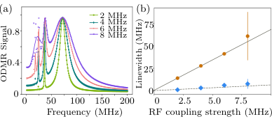
For the numerical simulation, we used the Lindblad master equation
| (25) |
here , drives the spin-lattice relaxation process, , is the Lindblad operator for the dephasing process, and are the Lindblad operators for the optical pumping Singh et al. 2022
, ,
, ,
, and is the optical pumping rate Singh et al. 2021.
The interaction Hamiltonian between the RF field and the spins is
where = represents the strength of the coupling to the RF field in frequency units and is the oscillation frequency of the field. Figure 12 shows the experimental and simulated ODMR spectra at 8 MHz RF coupling strengths with = 7 ms-1, = 10 s-1, and 185 ms-1; the simulated spectrum matches well with the experimentally recorded ODMR at 1 W RF power. Since we are using simple optical pumping model Singh et al. 2021, the amplitude of the simulated spectrum is normalized to the maximal ODMR contrast for the plot. For the simulated spectrum, we integrated Eq. (25) for 1.5 s for every frequency. Additional details can be found in our previous work Singh et al. 2022. Figure 13 (a) shows the simulated ODMR spectra at different RF coupling strengths with the same parameters used for simulating ODMR spectrum in Fig 12 except for the value of , which we reduced here to 2.5 to better resolve the multi-photon peaks.
| Peak | (MHz) | |
|---|---|---|
| 1 | 0.34 0.21 | 6.80 0.05 |
| 2 | 0 | 0.63 0.05 |
In Fig 13, with an RF coupling strength of 2 MHz, we can see 1-photon, and 2-photon peaks at 72 MHz and 36 MHz and a small signal of 3-photon peak at 24 MHz. At 8 MHz, the 5-, 4- and 3-photon peaks are also visible and close to each other, and therefore difficult to resolve. The linewidth of the 1- and 2-photon peaks are extracted by fitting the simulated ODMR to a sum of Lorentzians. Fig 13 (b) shows the resulting dependence of the linewidth vs. the square root of the RF power itogether with a fir to the function
| (26) |
The obtained fitting parameters, intercept and the slope are given in Table (3).
Appendix H: ODMR with different rf and laser powers
Figure 14 (a) shows the ODMR signal recorded for one of the high-contrast centers with different RF power, keeping the laser intensity at 184 kW/ cm² and (b) for different Laser intensity at 2 W RF power. At 9 W RF power, the ODMR signal contrast is 5.3 %, and the laser intensity does not affect the ODMR contrast significantly. In the course of recording these data, the PL count of the center fell from 8 kcps to 4 kcps which impacts the signal-to-noise ratio of the later recorded variable laser intensity ODMR spectra.
Acknowledgements.
This work was supported by the Deutsche Forschungsgemeinschaft in the frame of the ICRC TRR 160 (Project No. C7). J.U.H. acknowledge support from Swedish Research Council under VR grant No.2020-05444 and Knut and Alice Wallenberg Foundation (grant no. KAW 2018.0071). J.U.H. and F.K. acknowledge support from the European Union through the QuantERA grant InQuRe. F.K. acknowledges support from the German ministry of education and research (BMBF, grant no. 16KIS1639K, 16KISQ013 and 13N16219).References
- Koehl et al. (2011) W. F. Koehl, B. B. Buckley, F. J. Heremans, G. Calusine, and D. D. Awschalom, Room temperature coherent control of defect spin qubits in silicon carbide, Nature 479, 84 (2011).
- Kraus et al. (2013) H. Kraus, V. A. Soltamov, D. Riedel, S. Väth, F. Fuchs, A. Sperlich, P. G. Baranov, V. Dyakonov, and G. V. Astakhov, Room-temperature quantum microwave emitters based on spin defects in silicon carbide, Nature Physics 10, 157 (2013).
- Widmann et al. (2015) M. Widmann, S.-Y. Lee, T. Rendler, N. T. Son, H. Fedder, S. Paik, L.-P. Yang, N. Zhao, S. Yang, I. Booker, et al., Coherent control of single spins in silicon carbide at room temperature, Nature materials 14, 164 (2015).
- Nagy et al. (2019) R. Nagy, M. Niethammer, M. Widmann, Y.-C. Chen, P. Udvarhelyi, C. Bonato, J. U. Hassan, R. Karhu, I. G. Ivanov, N. T. Son, et al., High-fidelity spin and optical control of single silicon-vacancy centres in silicon carbide, Nature communications 10, 1954 (2019).
- Soltamov et al. (2012) V. A. Soltamov, A. A. Soltamova, P. G. Baranov, and I. I. Proskuryakov, Room temperature coherent spin alignment of silicon vacancies in - and -sic, Phys. Rev. Lett. 108, 226402 (2012).
- Riedel et al. (2012) D. Riedel, F. Fuchs, H. Kraus, S. Väth, A. Sperlich, V. Dyakonov, A. A. Soltamova, P. G. Baranov, V. A. Ilyin, and G. V. Astakhov, Resonant addressing and manipulation of silicon vacancy qubits in silicon carbide, Physical review letters 109, 226402 (2012).
- Singh et al. (2021) H. Singh, A. N. Anisimov, I. D. Breev, P. G. Baranov, and D. Suter, Optical spin initialization of spin- silicon vacancy centers in at room temperature, Phys. Rev. B 103, 104103 (2021).
- Carter et al. (2015) S. G. Carter, O. O. Soykal, P. Dev, S. E. Economou, and E. R. Glaser, Spin coherence and echo modulation of the silicon vacancy in at room temperature, Phys. Rev. B 92, 161202(R) (2015).
- Simin et al. (2017) D. Simin, H. Kraus, A. Sperlich, T. Ohshima, G. V. Astakhov, and V. Dyakonov, Locking of electron spin coherence above 20 ms in natural silicon carbide, Phys. Rev. B 95, 161201(R) (2017).
- Christle et al. (2015) D. J. Christle, A. L. Falk, P. Andrich, P. V. Klimov, J. U. Hassan, N. T. Son, E. Janzén, T. Ohshima, and D. D. Awschalom, Isolated electron spins in silicon carbide with millisecond coherence times, Nature materials 14, 160 (2015).
- Singh et al. (2020) H. Singh, A. N. Anisimov, S. S. Nagalyuk, E. N. Mokhov, P. G. Baranov, and D. Suter, Experimental characterization of spin-3/2 silicon vacancy centers in -sic, Phys. Rev. B 101, 134110 (2020).
- Lekavicius et al. (2022) I. Lekavicius, R.L. Myers-Ward, D.J. Pennachio, J.R. Hajzus, D.K. Gaskill, A.P. Purdy, A.L. Yeats, P.G. Brereton, E.R. Glaser, T.L. Reinecke, and S.G. Carter, Orders of magnitude improvement in coherence of silicon-vacancy ensembles in isotopically purified -, PRX Quantum 3, 010343 (2022).
- Udvarhelyi et al. (2020) P. Udvarhelyi, G. m. H. Thiering, N. Morioka, C. Babin, F. Kaiser, D. Lukin, T. Ohshima, J. Ul-Hassan, N. T. Son, J. Vučković, J. Wrachtrup, and A. Gali, Vibronic states and their effect on the temperature and strain dependence of silicon-vacancy qubits in -, Phys. Rev. Applied 13, 054017 (2020).
- Shang et al. (2020) Z. Shang, A. Hashemi, Y. Berencén, H.-P. Komsa, P. Erhart, S. Zhou, M. Helm, A. V. Krasheninnikov, and G. V. Astakhov, Local vibrational modes of si vacancy spin qubits in sic, Phys. Rev. B 101, 144109 (2020).
- Anisimov et al. (2016) A. Anisimov, D. Simin, V. A. Soltamov, S. P. Lebedev, P. G. Baranov, G. V. Astakhov, and V. Dyakonov, Optical thermometry based on level anticrossing in silicon carbide, Scientific reports 6, 33301 (2016).
- Abraham et al. (2021) J. B. S. Abraham, C. Gutgsell, D. Todorovski, S. Sperling, J. E. Epstein, B. S. Tien-Street, T. M. Sweeney, J. J. Wathen, E. A. Pogue, P. G. Brereton, T. M. McQueen, W. Frey, B. D. Clader, and R. Osiander, Nanotesla magnetometry with the silicon vacancy in silicon carbide, Phys. Rev. Appl. 15, 064022 (2021).
- Soltamov et al. (2019) V. A. Soltamov, C. Kasper, A. V. Poshakinskiy, A. N. Anisimov, E. N. Mokhov, A. Sperlich, S. A. Tarasenko, P. G. Baranov, G. V. Astakhov, and V. Dyakonov, Excitation and coherent control of spin qudit modes in silicon carbide at room temperature, Nature Communications 10, 1678 (2019).
- Taylor et al. (2008) J. M. Taylor, P. Cappellaro, L. Childress, L. Jiang, D. Budker, P. Hemmer, A. Yacoby, R. Walsworth, and M. Lukin, High-sensitivity diamond magnetometer with nanoscale resolution, Nature Physics 4, 810 (2008).
- Fuchs et al. (2015) F. Fuchs, B. Stender, M. Trupke, D. Simin, J. Pflaum, V. Dyakonov, and G. Astakhov, Engineering near-infrared single-photon emitters with optically active spins in ultrapure silicon carbide, Nature communications 6, 1 (2015).
- Hain et al. (2014) T. C. Hain, F. Fuchs, V. A. Soltamov, P. G. Baranov, G. V. Astakhov, T. Hertel, and V. Dyakonov, Excitation and recombination dynamics of vacancy-related spin centers in silicon carbide, Journal of Applied Physics 115, 133508 (2014), https://doi.org/10.1063/1.4870456 .
- Kasper et al. (2020) C. Kasper, D. Klenkert, Z. Shang, D. Simin, A. Gottscholl, A. Sperlich, H. Kraus, C. Schneider, S. Zhou, M. Trupke, W. Kada, T. Ohshima, V. Dyakonov, and G. V. Astakhov, Influence of irradiation on defect spin coherence in silicon carbide, Phys. Rev. Appl. 13, 044054 (2020).
- Hornos et al. (2011) T. Hornos, A. Gali, and B. G. Svensson, Large-scale electronic structure calculations of vacancies in 4h-sic using the heyd-scuseria-ernzerhof screened hybrid density functional, in Materials Science Forum, Vol. 679 (Trans Tech Publ, 2011) pp. 261–264.
- Babin et al. (2022) C. Babin, R. Stöhr, N. Morioka, T. Linkewitz, T. Steidl, R. Wörnle, D. Liu, E. Hesselmeier, V. Vorobyov, A. Denisenko, et al., Fabrication and nanophotonic waveguide integration of silicon carbide colour centres with preserved spin-optical coherence, Nature materials 21, 67 (2022).
- Wang et al. (2017) J. Wang, X. Zhang, Y. Zhou, K. Li, Z. Wang, P. Peddibhotla, F. Liu, S. Bauerdick, A. Rudzinski, Z. Liu, et al., Scalable fabrication of single silicon vacancy defect arrays in silicon carbide using focused ion beam, Acs Photonics 4, 1054 (2017).
- Pavunny et al. (2021) S. P. Pavunny, A. L. Yeats, H. B. Banks, E. Bielejec, R. L. Myers-Ward, M. T. DeJarld, A. S. Bracker, D. K. Gaskill, and S. G. Carter, Arrays of si vacancies in 4h-sic produced by focused li ion beam implantation, Scientific reports 11, 1 (2021).
- Ivády et al. (2017) V. Ivády, J. Davidsson, N. T. Son, T. Ohshima, I. A. Abrikosov, and A. Gali, Identification of si-vacancy related room-temperature qubits in silicon carbide, Phys. Rev. B 96, 161114(R) (2017).
- Baranov et al. (2011) P. G. Baranov, A. P. Bundakova, A. A. Soltamova, S. B. Orlinskii, I. V. Borovykh, R. Zondervan, R. Verberk, and J. Schmidt, Silicon vacancy in sic as a promising quantum system for single-defect and single-photon spectroscopy, Phys. Rev. B 83, 125203 (2011).
- Fox et al. (2006) A. M. Fox, M. Fox, et al., Quantum optics: an introduction, Vol. 15 (Oxford university press, 2006).
- Basché et al. (1992) T. Basché, W. E. Moerner, M. Orrit, and H. Talon, Photon antibunching in the fluorescence of a single dye molecule trapped in a solid, Phys. Rev. Lett. 69, 1516 (1992).
- Neu et al. (2011) E. Neu, D. Steinmetz, J. Riedrich-Möller, S. Gsell, M. Fischer, M. Schreck, and C. Becher, Single photon emission from silicon-vacancy colour centres in chemical vapour deposition nano-diamonds on iridium, New Journal of Physics 13, 025012 (2011).
- Kasper (2021) C. A. Kasper, Engineering of Highly Coherent Silicon Vacancy Defects in Silicon Carbide, Ph.D. thesis, Universität Würzburg (2021).
- Morioka et al. (2022) N. Morioka, D. Liu, O. O. Soykal, I. Gediz, C. Babin, R. Stöhr, T. Ohshima, N. T. Son, J. Ul-Hassan, F. Kaiser, and J. Wrachtrup, Spin-optical dynamics and quantum efficiency of a single v1 center in silicon carbide, Phys. Rev. Appl. 17, 054005 (2022).
- Suter (2020) D. Suter, Optical detection of magnetic resonance, Magnetic Resonance 1, 115 (2020).
- Suter and Jelezko (2017) D. Suter and F. Jelezko, Single-spin magnetic resonance in the nitrogen-vacancy center of diamond, Progress in Nuclear Magnetic Resonance Spectroscopy 98-99, 50 (2017).
- Singh et al. (2022) H. Singh, M. A. Hollberg, A. N. Anisimov, P. G. Baranov, and D. Suter, Multi-photon multi-quantum transitions in the spin- silicon-vacancy centers of sic, Phys. Rev. Research 4, 023022 (2022).
- Wertz (2012) J. Wertz, Electron spin resonance: elementary theory and practical applications (Springer Science & Business Media, 2012).
- Jensen et al. (2013) K. Jensen, V. M. Acosta, A. Jarmola, and D. Budker, Light narrowing of magnetic resonances in ensembles of nitrogen-vacancy centers in diamond, Phys. Rev. B 87, 014115 (2013).
- Bourassa et al. (2020) A. Bourassa, C. P. Anderson, K. C. Miao, M. Onizhuk, H. Ma, A. L. Crook, H. Abe, J. Ul-Hassan, T. Ohshima, N. T. Son, et al., Entanglement and control of single nuclear spins in isotopically engineered silicon carbide, Nature Materials 19, 1319 (2020).
- Bulancea-Lindvall et al. (2021) O. Bulancea-Lindvall, N. T. Son, I. A. Abrikosov, and V. Ivády, Dipolar spin relaxation of divacancy qubits in silicon carbide, npj Computational Materials 7, 213 (2021).
- Wolfowicz et al. (2017) G. Wolfowicz, C. P. Anderson, A. L. Yeats, S. J. Whiteley, J. Niklas, O. G. Poluektov, F. J. Heremans, and D. D. Awschalom, Optical charge state control of spin defects in 4h-sic, Nature communications 8, 1 (2017).
- Wang et al. (2019) J.-F. Wang, Q. Li, F.-F. Yan, H. Liu, G.-P. Guo, W.-P. Zhang, X. Zhou, L.-P. Guo, Z.-H. Lin, J.-M. Cui, et al., On-demand generation of single silicon vacancy defects in silicon carbide, Acs Photonics 6, 1736 (2019).
- Glenn et al. (2015) D. R. Glenn, K. Lee, H. Park, R. Weissleder, A. Yacoby, M. D. Lukin, H. Lee, R. L. Walsworth, and C. B. Connolly, Single-cell magnetic imaging using a quantum diamond microscope, Nature methods 12, 736 (2015).
- Glenn et al. (2018) D. R. Glenn, D. B. Bucher, J. Lee, M. D. Lukin, H. Park, and R. L. Walsworth, High-resolution magnetic resonance spectroscopy using a solid-state spin sensor, Nature 555, 351 (2018).
- Bucher et al. (2020) D. B. Bucher, D. R. Glenn, H. Park, M. D. Lukin, and R. L. Walsworth, Hyperpolarization-enhanced nmr spectroscopy with femtomole sensitivity using quantum defects in diamond, Phys. Rev. X 10, 021053 (2020).