Masterarbeit in Astrophysik
angefertigt im Max Planck Institut für Radioastronomie
vorgelegt der
Mathematisch-Naturwissenschaftlichen Fakultät
der
Rheinischen Friedrich-Wilhelms-Universität
Bonn
August 2019
I hereby declare that this thesis was formulated by myself and that no sources or tools other than those cited were used.
| Bonn, | . | . |
|---|---|---|
| Date | Signature |
| 1. Gutachter: | Prof. Dr. Frank Bertoldi |
| 2. Gutachter: | PD. Dr. Jürgen Kerp |
Optimizing digital spectrometers for radioastronomical observations
Acknowledgements
First of all I would like to thank Prof. Dr. Frank Bertoldi for being my first referee and giving me the opportunity to write this Master-thesis with a focus on instrumentation. Secondly many thanks also to Prof. Dr. Bernd Klein for the possibility to work with the spectrometers developed at the DSP-division of the Max-Planck-Institut für Radioastronomie (MPIfR).
I have to thank the whole DSP division of the MPIfR for making this experience an interesting one and providing a pleasant working atmosphere. A very special word of thanks goes to Stefan Hochgürtel for being a superb supervisor, for always being willing to listen to my problems and for giving important feedback at all stages of this thesis.
Furthermore I want to thank my friends and fellow students for the unforgettable journey up to now and all the journeys still to come. Zu guter Letzt möchte ich meinen Eltern danken für eure immerwährende Unterstützung in jeder Lebenslage. Ohne euch wäre ich nicht die Person die ich bin und hätte sicher nicht diese Arbeit geschrieben.
Chapter 1 Introduction
Since the beginning of mankind the sky is a mystery and has a strong attraction for the human mind. For a long time the sky was only observable in the optical regime (). The next window, which gave mankind a new picture of the sky, was the radio regime. In 1931 the first radioastronomical observation was performed unintentionally by Karl Jansky. He searched for the source of static noise in transatlantic telecommunication. After observations with a directional antenna at he discovered, that a part of the noise originates from Milky Way, especially from the center of our galaxy. Inspired by the work of Jansky, Grote Reber built a parabolic dish with in diameter by himself. In 1938 he successfully observed the radio sky at . Since then the instruments became more and more powerful and new techniques were developed to observe at higher frequencies. Today observations in the sub-mm regime up to circa are possible [1].
Since the discovery of the Fraunhofer lines spectroscopy is a major technique in astronomy, not only in the optical regime but over all wavelengths. An important aspect of spectroscopy is the identification of spectral lines and therefore the revelation of the chemical composition and physical conditions of an astronomical source. In the optical regime spectral lines of atoms dominate. But in the sub-mm regime molecular lines dominate the spectra. There fore radioastronomical spectroscopy allows deep studies of molecular clouds, the birthplaces of stars.
Radioastronomical spectrometers can be implemented by a number of different technologies. An analog filter bank is comparable to photometry with filters in the optical range. This type of spectrometer is rather unstable as the analog components drift. Furthermore the matching between the different spectral channels is challenging. The usual number of spectral channels lies between and for analog filter banks.
Autocorrelation spectrometers form the power spectrum from the autocorrelation of the input signal. The power spectrum is the Fourier transform of the autocorrelation. The autocorrelation can be implemented in the analog or digital regime. Analog implementations achieve a greater bandwidth ( with spectral channels [2]), while digital ones are more stable and offer more spectral channels ( with spectral channels [3]).
The acousto-optical spectrometer uses acoustic waves in a crystal to diffract a laser beam, which then carries the information of the power spectrum. The incoming radio signal is coupled into the crystal. The laser beam is then projected onto a CCD, which records the resulting spectrum. They provide up to of bandwidth with a resolution of [4]. These spectrometers are especially sensitive to mechanical and thermal drifts due to the optics.
The chirp transform spectrometer uses sonic wave propagation in crystals to calculate the power spectrum with the help of the velocity dispersion of those waves. These spectrometers are optimized for spectral resolution in the order of , but the bandwidth is limited to [5].
fast Fourier transform spectrometers (FFTSs) calculate the power spectrum, using a fast Fourier transform (FFT) to get the complex amplitude spectrum, which is squared to get the power spectrum. FFTSs achieve a bandwidth of with up to channels.
FFTSs are the newest type of spectrometer for radioastronomical receivers. This thesis has been written at the DSP-devision of the MPIfR, which is a leading developer of FFTSs. The FFTSs developed at the MPIfR use field programmable gate arrays (FPGAs) to process digital signals from analog digital converters (ADCs). The development of these FFTSs was possible due to new generations of ADCs with sample rates of multiple and the increasing computational power of FPGAs. Due to a little number of analog components this type of spectrometer is quite stable in terms of drifts.
However there are also limiting components in FFTSs, which can be optimized. One is the ADC, and its limiting characteristics shall be reduced in this thesis. The ADCs on the spectrometers are composed of a number of slower ADCs, which slightly differ from each other (see chapter 10). A calibration procedure has to correct these differences for an optimal performance of the spectrometers. For small bandwidths these differences can be assumed to be frequency independent, but for larger bandwidths this assumption reduces the dynamical range of the spectrometers. The current generation of FFTSs calibrates these differences at a fixed frequency with a statistical approach (see chapter 4.2 of [7]). The goal of this thesis is to develop and implement a method in the FFTSs to correct for these differences in a frequency dependent manner. This correction shall enhance the dynamical range of the spectrometer and shall allow further advancement in the development of FFTSs.
This thesis starts with a short introduction to spectroscopic radioastronomy in chapter 2. Chapter 3 first describes the mathematical tools used in this thesis, then it describes the ADCs used on the spectrometers. Chapter 4 gives a brief overview over the hardware of used to measure the differences between different signal paths. A method to characterize these differences is described in chapter 5. Chapter 6 discusses different approaches to correct these differences. In chapter 7 the implementation details of the chosen approach in the spectrometers are discussed. The implementation is tested and characterized, especially in terms of stability over time and temperature. The conclusion in chapter 8 summarizes the work and presents prospects for other application cases and further improvements.
Chapter 2 Fundamentals of spectroscopic radioastronomy
Distant objects can only be investigated by messengers they emit or interact with. Only a few messengers can be received from these objects. Currently these messengers are neutrinos, gravitational waves and electromagnetic radiation. The latter can be divided into different regimes, which corresponds to photons with distinct wavelengths respectively energies (see table 1 for a short overview and figure 1 for a graphically representation). Each regime reveals different information about the objects in the universe. For a complete understanding of the universe the information from all messengers and regimes are essential.
| Regime | Wavelength | Energy | Observable from the ground | |
|---|---|---|---|---|
| Radio | to | to | yes | |
| mm and sub-mm | to | only at high altitudes | ||
| Far infrared | no | |||
| Near infrared | to | to | yes | |
| Optical | yes | |||
| Ultra violet | to | no | ||
| X-ray | no | |||
| -ray | below | above | not directly |
Each messenger and regime hold their own challenges. For example neutrinos have a tiny cross section, hence the detection of neutrinos need massive detectors. In the X-ray and -ray regime conventional mirrors have no effect, therefore mirrors based on total reflection are used. The radio regime, mm and sub-mm have wavelengths from to . A single telescope in the radio regime has an angular resolution which is not comparable to the one of optical telescopes, because the maximal size of radio telescopes is limited due to constructive issues. This lead to the development of interferometry, where the signals from different telescopes are combined to achieve a better angular resolution. Furthermore the commercial and military use of frequencies in the radio regime causes radio frequency interference (RFI). The sub-mm regime is sensitive to the column of water in the atmosphere along the line of sight. Therefore telescope for this regime are placed at high and dry location (e.g. Atacama Desert in Chile for the Atacama Pathfinder Experiment (APEX)). Another solutions are airborne or spaceborne telescopes. Balloon experiments and plane based experiment give easier excess for maintenance and upgrade compared to satellites but suffer from the residual atmosphere. Another challenge is the handling of signals at these high frequencies. This becomes even more challenging in the regime of far infrared.
1 A simple radio-telescope
A radio-telescope is composed from different parts. In the following the most important parts are described in the order as they appear in the signal path.
The first element is an antenna, which collects the signal and couples it into a transfer element (e.g. coax-cable or waveguide). A typical antenna configuration is a parabolic dish which focuses the incoming planar waves into the feed where the wave is picked up by a short wire. Figure 2(a) shows such an antenna configuration. The electromagnetic waves propagate in a coax cable or a wave-guide to an amplifier. This amplifier is used to increase the signal amplitude. The amplification decreases the influence of noise (e.g. thermal noise), which is introduced by the following components. The signal is then filtered to prevent contamination with RFI. This filtered signal is then mixed with a local oscillator (LO) to a lower frequency range, where the further signal processing is easier. This part of the signal processing chain is the frontend, more precise it is a Heterodyne receiver. A Heterodyne receiver preserves the phase information of the received waves. Receivers, which preserves the phase information are called coherent.
The further treatment of the signal, which is called backend, depends on the purpose of the observation. The simplest backend is a total power backend. This backend measures the total power of the received radiation in the frequency band of the receiver. Figure 2(b) shows a simple total power receiver (consisting of a frontend and a total power backend). A spectrometer backend is similar to a total power backend. But instead of the power of the whole band, the spectrometer measures the power in a number of smaller bands (frequency channels).
The phase information, which is preserved in coherent receivers, can be used for beam forming and interferometry. Both techniques use a number of antennas to achieve a better angular resolution.
In contrast to the Heterodyne receiver bolometers are incoherent receivers. The basic idea is to detect photons based on their energy. The simplest bolometer is a black body connected to a heat reservoir (with a known thermal resistance between black body and reservoir). The temperature difference between black body and reservoir is then related to the absorbed radiation. Today bolometer technologies exists, which do not relay on the temperature (e.g. microwave kinetic inductance detector (MKID) see 3) but on other absorption mechanism of photons.
2 Spectroscopy in the sub-mm regime
FFTSs are the preferred implementation to realize high spectral resolution over wide bands. An FFTS processes the mixed down signal in the digital regime. Therefore an ADC converts the analog intermediate frequency (IF) signal to a digital datastream. An FFT transforms this time-domain datastream into a complex spectrum, which is squared to get the power spectrum. Finally the power spectra are summed up to perform an integration over time. The basic principle of an FFTS is shown in figure 3 in contrast to an autocorrelation spectrometer. An autocorrelation spectrometer first computes the autocorrelation function of the time-domain signal, which is then integrated and finally converted into the power spectrum with an FFT.
The high frequency of the radio frequency (RF) signals in the sub-mm regime are technologically challenging, which requires a different setup for a receiver than the one given in chapter 1. Currently no amplifiers are available for such frequencies. Therefore the RF signal is filtered and mixed down into the IF band, which is typically to . The RF cannot be mixed into the band between and as the technologies of these mixers do not support to couple out low frequency signals. The IF signal is then amplified and filtered further. In a second mixing stage the IF signal is translated into the baseband ( to ). This baseband signal is then sampled by the spectrometer. Figure 4(a) shows the schematics of such a receiver.
The bandwidths of FFTSs are increasing, due to the advances of ADC development.
For example the ADC ADC12DJ3200 has an analog input bandwidth of [13].
This increasing analog input bandwidth means, that the FFTS is not only sensitive in the baseband () but also in the second Nyquist-band ().
Therefore the second mixing stage can be skipped and the FFTS can directly sample the IF signal.
Such a receiver is shown in figure 4(b).
This simplification of the receiver chain, leads to a more stable system.
Furthermore it consumes less power, space and money.
2.1 Multi-beam heterodyne receivers
In optical observations different positions at the sky are observed simultaneously due to a number of pixels in the focal plane. A similar concept is developing for heterodyne receivers. For this an array of feeds is placed in the focal plane. The output of each feed is treated separately in the signal processing (filtering, amplifying, mixing and digitalization).
An example for such a design is the CCAT-prime Heterodyne Array Instrument (CHAI) at the Cerro Chajnantor Atacama Telescope-prime (CCAT-prime) telescope, which is located at the Atacama desert of northern Chile and is conceived as survey telescope. It is a ground based instrument operating at submillimeter to millimeter wavelengths [14] with opening. CHAI is composed of two separate receivers. One operating at a lower frequency range of and one at a higher frequency range of . The primary science targets is the star forming in the interstellar medium. This is covered by the observation of CI fine-structure transitions and , as well as the rotational transitions and of CO. Each of the two receivers consists of pixels at first light. A possible extension to pixels each is planned. The Multi-beam approach increases the mapping speed of the instrument, which will lead to a very powerful and fast survey instrument. The limiting factor for the number of pixels is the cost per pixel and the space available at the telescope site [15]. Each pixel needs the complete signal processing chain. Therefore the costs of each part of the chain has to be optimized, including the used spectrometers. Furthermore the complexity of the system has to be minimized to make such a project feasible, luckily both requirements go hand in hand most of the time. On important point of improvement is the elimination of the IF system, as this reduces the number of needed mixer and removes one complete stage of the signal chain. Therefore the backends have to operate between and instead of . Another requirement is the available space at the telescope site, which is limited. With the elimination of the IF system, its space can be used by other components of the receiver.
All this requirements have to be balanced to successfully implement a project like this. The current planed solution to this situation is a qFFTS-8G with four inputs per spectrometer, which can operate between and from . With a qFFTS-8G between and spectrometer are needed.
3 Microwave kinetic inductance detectors
MKIDs are superconducting devices to detect photons. Their surface impedance changes when they absorb a photon. This effect is based on the creation of quasi-particles by incident radiation. This quasi-particles block energy states, which would be occupied with Cooper pairs otherwise (due to the exclusion principle). This blocking leads to a change in the impedance. Figure 5 shows the energy states of such a system, where a Cooper pair is broken up by a photon.
MKIDs are non coherent receivers as the phase of the photons is lost in the receiving process. The sensitive bandwidth is given by the optics and filter in front of the MKIDs and the minimum energy to create a quasi-particle ( is the superconducting gap energy) [18]. Consequently, these detectors are sensitive to a larger bandwidth than heterodyne receivers; but the spectral resolution, if an energy measurement of the photons is implemented, is worse than a heterodyne receiver combined with a spectrometer.
The surface impedance of MKIDs is mostly inductive. The measurement of the changing surface impedance is done with a superconducting resonant circuit. The MKID is connected to a capacity, the resonance frequency of the circuit consisting of the capacity and MKID changes with the surface impedance of the MKID. Figure 6(a) shows a schematic representation of such a resonant circuit, while figure 6(b) presents a real implementation of MKIDs, which are coupled to one readout line. The typical readout of a MKID is done via the phase or amplitude change of an applied sinusoid-signal at the reference frequency. Figures 7(a) and 7(b) show the amplitude change and phase change due to a resonance change. Compared to the measurement of the position of the resonance frequency this is more sensitive to changes and only needs one applied frequency instead of a frequency sweep.
MKIDs can be produced, together with the capacities, in thin-film lithography. Therefore an array of MKID pixels can be produced with conventional optical lithography, which reduces the costs per pixel compared to other pixel technologies. The different pixels are multiplexed in the the frequency domain. This means that each pixel has a different resonance frequency. Up to pixels can be read out via one readout line in figure 6(a). A digital analog converter (DAC) generates a signal with a frequency component for each pixel. This signal is applied to one side of the readout line, on the other side a spectrometer is connected, which measures the amplitude and phase of the frequency components. From these information the resonance frequency of the circuits can be derived and from there the absorbed radiation.
The increasing bandwidths of FFTSs allow to increase the number of pixels per readout line or to reduce the number of spectrometer per readout line. This simplifies the overall design and reduces space, power and cost requirements.
Chapter 3 Digital signal processing theory
Digital signal processing (DSP) allows the transformation and analysis of digital signals. In this context a digital signal is a signal which is discrete in time and amplitude. These can be implemented in digital circuits like an FPGA or a central processing unit (CPU). Compared to analog signal processing, the digital counterpart has different advantages:
- •
More stable: Analog filters vary over time due to different environmental parameters. After the digitalization the signals and transformations are not sensitive to such drifts any more.
- •
Changeable after deployment: It is possible to program most processing units, like FPGAs or CPUs, after an instrument is deployed.
- •
Better footprint scaling: The footprint of DSP circuits scales better than the footprint of analog circuits. E.g. generating amplitude spectrum needs an sophisticated analog filter for each channel; while the digital counterpart is composed of a few integrated circuits (ICs).
The downside is the need of high processing power and the possible loss of information due to discretization. But due to the exponential development of the processing power in the last decades, the processing power is on hand. By designing the signal processing chain carefully, in both regimes the analog and digital, an unwanted information loss can be constrained.
In the digital domain clocks are used to synchronize different components and their processes. In most cases these signals are square wave to archive a low errors in the synchronization between the components. Either the rising edge, falling edge or both are used for clocking. In the figures of this thesis the the rising edge will be used.
A function, continuous with respect to its argument, is represented by the notation . is instead used for a function discrete in terms of , where is the index of the sample.
4 Complex numbers
The complex numbers are an extension of the real numbers. This is done by defining a solution for negative square roots , the imaginary unit. Less abstract the one dimensional number line of the real numbers is extended by a second dimension. A complex number can be represented by two real numbers, the real part and the imaginary part .
The complex plain, in which the complex numbers are living, is typically described by rectangular coordinates () or by polar coordinates (). The transformation from rectangular coordinates to polar ones is given as follows:
| (1) | ||||
| (2) |
The transformation other way round is given as follows:
| (3) |
In terms of DSP the angle of a complex number corresponds to the phase of a signal and the absolute value corresponds to the amplitude of the signal.
5 Fourier transform
The continuous Fourier transform of a function is defined as:
| (4) |
The Fourier transform can be used to transform functions between a representation in time and in frequency . In general both representations live in the complex plain. In this thesis the Fourier pairs are notated by lower case and capital letters, for example as the Fourier pair of . A shift in time corresponds to a phase shift in the frequency domain. For a function that is shifted in time by , the following applies:
| (5) | ||||
| (6) | ||||
Hence a shift in time corresponds to a phase shift, which depends on the frequency of the component.
In the regime of DSP there are no continuous signals but time discrete signals, which are a sequence of single samples. Therefore the discrete Fourier transform (DFT) is used instead of the continuous Fourier transformation. A DFT on samples leads to a spectrum of length . The -th channel of the DFT is defined similar to the continuous one:
| (7) |
The notation is used in this thesis for a DFT of the sequence . The calculation of a spectrum of length needs operation with the DFT algorithm. The complexity of the DFT algorithm is . Therefore the number of operations scales as , relative to the length of a spectrum.
From the definition of the DFT follows its linearity. The periodicity of the complex exponential function leads to a periodicity of the DFT, each channels:
| (8) | ||||
A typical digitized signal has no imaginary contribution, therefore it is real. This leads to another symmetry of the DFT. When ():
| (9) | ||||
The calculation of a DFT can be sped up by some optimizations. A popular algorithm is the FFT for DFTs with a length of . That allows to split up the calculation into two parts. The even samples and the odd ones,
| (10) | ||||
where results from the DFT of the even samples and from the DFT of the odd samples.
Using the periodicity of the DFT of length , the second half of the spectrum can be calculated ():
| (11) | ||||
| (12) |
The smaller DFTs and can be calculated the same way, down to a DFT of length :
| (13) | ||||
The number of needed operations for a FFT of size without the calculation of the smaller spectra is . The whole calculation needs iterations to reach a spectrum length of which is trivial to calculate. This leads to a complexity of for the FFT.
6 Convolution
A continuous convolution is given by
| (14) |
Under a Fourier transform a convolution transforms as follows:
| (15) | ||||
The linear discrete convolution corresponds to the continuous convolution. For two signals of length and of length the linear discrete convolution is defined as follows:
| (16) |
has the value for and . The resulting signal has a length of . If the the series is -periodic () then the linear discrete convolution is also -periodic:
| (17) |
Furthermore a circular discrete convolution exists. Its definition, with two signals of length and of length , is as follows:
| (18) |
The result has again a length of . Due to the modulus operation the additional samples, which occur at the linear convolution, are summed up with the other ones. The circular discrete convolution is connected to the DFT, similar to the relationship between Fourier transform and continuous convolution:
| (19) | ||||
Due to the low complexity of the FFT this enables fast circular convolutions for long input series. In general the circular discrete convolution and the linear discrete convolution generate different output series for the same input. But in the case of a series of length and an -periodic series () both, the linear discrete convolution and the circular discrete convolution, yield the same result:
| (20) |
Furthermore the circular discrete convolution can be used to compute the linear discrete convolution between a kernel of length and a longer signal of length , [21]. The basic idea is to split up the signal in overlapping chunks and use the following:
| (21) |
Hence the calculation of linear convolutions with long input series can be sped up with the use of an FFT, too.
7 Sampling theorem
The sampling converts a time-continuous signal into a time-discrete series. It is one of the premises for DSP as it only operates on time-discrete series. The sampling can be represented by a multiplication with an impulse train (for the transform of see chapter 2.2 of [22]):
| (22) | ||||
| (23) |
The time-continuous input signal is . Therefore the signal after the sampling, , is
| (24) | ||||
| (25) | ||||
From the last equation it is obvious that can contain an infinite number of frequency components from the time-continuous signal . Figure 8 shows this effect for a sampling with of two sinusoidal signals with and . At the sample points both signals have the same value and are not distinguishable after the sampling. To get an unambiguous spectrum the input signal has to be confirmed in the frequency region to ; this region is called -th Nyquist-band. If the signal is not limited to a bandwidth of , different frequency components of the continuous signal are summed up in one frequency of the time discrete signal. Figure 9 illustrates this in the frequency domain. If the Nyquist-sampling is not fulfilled the (upper part) different frequency components are summed up. This effect is called aliasing. The unaliased signal cannot be restored from the sampled data. To get a not aliased sampled signal, analog filters are needed before the sampling process (Anti-Aliasing-Filter) to limit the bandwidth of the continuous signal.
8 Linear digital filter
Digital filters are the analogue to analog filter. They can be characterized by their impulse response. The impulse response is the output of a filter after a Dirac-Impulse . Two groups of linear digital filters are distinguished
- •
Finite impulse response filter (FIR-Filter)
- •
Infinite impulse response filter (IIR-Filter)
They differ in the length of their impulse response. An FIR-Filter has a finite impulse response. Therefore its output only depends on a finite number of input samples and is after samples of value . These samples are saved in memory. As there is no feedback in this architecture, FIR-Filter are stable under all conditions. An FIR-Filter of length with input , output and coefficients can be defined as follows:
| (26) |
Figure 10 represents a FIR-Filter of length . The length of a FIR-Filter is sometimes also called number of taps. An FIR-Filter with taps is a filter with a length of . A FIR-Filter corresponds to a linear convolution:
| (27) |
An IIR-Filter has an infinite impulse response, the output of the filter depends on all inputs samples, which have been processed by the filter. As the memory to save samples is limited, IIR-Filter use their output as second input (next to the sample which is to be processed). This feedback can lead to instabilities of the filter (e.g. behavior which depends strongly on the initial conditions and can lead to periodic behavior). There are algorithms to generate coefficients for stable IIR-Filters, but the quantization of these coefficients can lead again to instable filters. Therefore the coefficients have to be checked after the quantization. An IIR-Filter with input , output and coefficients , coefficients can be defined as follows:
| (28) |
Figure 11 shows an IIR-Filter with .
The transfer function describes the changes in phase and amplitude of a signal component with frequency due to a filter. For digital filters the coefficients of a filter determine the corresponding transfer function. The transfer function at frequency bin of a a FIR-Filter with coefficients is given by the following:
| (29) |
The transfer function between the points is given by a -interpolation.
9 Analog digital converter
The ADC is an electronic device to convert an analog signal (continuous in time and value) into a digital signal (discrete in time and value). An ADC consists of a sample and hold stage (S/H-stage) followed by a converter unit. The S/H-stage stores the amplitude of the analog signal at one time; this element is responsible for the discretization in time. Figure 12(a) shows a simple S/H-stage circuit. The sampling frequency is given in (samples per second). This stored amplitude is then converted into a digital value of a certain bit-width by the converter unit; this element is responsible for the discretization in amplitude. This is always relative to an upper and lower reference voltage (e.g. and ). Only amplitudes between these two are valid.
A common type of ADC is a FLASH-ADC. Its converter is implemented by an array of comparators with different threshold voltages. These are followed by an encoding logic which converts the comparator outputs to a binary number. A simple -bit version of this type is shown in figure 12(b).
An ADC can be represented by a filter, with a transfer function, followed by a S/H-stage. An input signal is changed due to the transfer function of the ADC as follows:
| (30) | ||||
| (31) |
The S/H-stage is responsible for the sampling of the time-continuous signal. It corresponds to a multiplication of with an impulse train . The combination of both stages, the filter and the S/H-stage, results in a digital signal as follows:
| (32) | ||||
| (33) | ||||
The gain and phase alterations of the sampled signal with frequency is connected to the transfer function of the ADC:
| (34) | ||||
| (35) | ||||
| (36) |
9.1 Quantization error
The quantization maps a range of continuous values to one discrete value . This may cause a difference between discrete and continuous value, which is called quantization error. The statistical properties of this error can be derived under the assumption that the difference is uniformly distributed. The probability density of each difference is determined by the normalization of the probability.
| (37) | ||||
| (38) |
The mean of this error is obviously zero (). The standard deviation is derived as follows:
| (39) | ||||
Hence the error (or the noise) due to the quantization depends quadratically on the step size of the quantization.
10 Time interleaved ADC
The sampling rate and the conversion rate of ADCs are limited. To achieve higher rates ADCs () can be combined into a time interleaved ADC (TIADC), where each ADC samples with a frequency of . A single ADC within a TIADC is called ADC-Core. The clock for each ADC-Core (, ) is shifted by or with respect to the phase of the input clock of the TIADC. Figure 13 shows this schematically for an ideal TIADC with ADC-Cores. Figure 40 shows the input signals (clock and signal) for such a TIADC together with the phase shifted clock for each ADC-Core and the output of the corresponding S/H-stages. The S/H-stages in front of the ADC-Cores have to be fast enough to sample at the total sample rate of the TIADC . Yet the following parts of each ADC-Core only run at .
Each ADC-Core differs from the others (e.g. gain, offset, phase shift of input signal). An offset of an ADC-Core shifts the whole signal by a constant voltage. As the offset is constant it does not depend on the frequency of the input signal. Hence offsets between the ADC-Cores are frequency independent mismatches.
Gain and phase mismatches can most easily be explained by the example of a sinusoidal signal, which is applied to the TIADC. In the case of gain mismatches the different ADC-Cores sample sinusoidal signals with different amplitudes. In the case of phase mismatches the different ADC-Cores sample sinusoidal signals, which are shifted against each other in time. The phase and gain mismatches between ADC-Cores can change with the frequency of the applied sinusoidal signal. Therefore these are frequency dependent mismatches. For a general signal, each frequency component of the signal is affected differently, depending on the frequency behavior of the gain and phase mismatches. These two mismatches can be described by one complex number, as the gain and phase are the representation in polar coordinates.
An offset mismatch between ADC-Cores leads to spurs at the frequencies . Whereas gain and phase mismatches create mirror signals of a signal with frequency at the frequencies [19]. Figure 14 shows a spectrum with spurs due to phase and gain mismatches in comparison to the unaffected spectrum.
ADC-Cores within a TIADC often allow to trim their offset, gain and phase. But a single setting to trim these may not be sufficient for all frequencies; especially if high bandwidths or higher Nyquist-bands are needed. Therefore a frequency dependent correction of phase and gain is highly advisable.
TIADCs can be implemented in one IC (e.g. ADC12DJ3200 [13]) or by using more than one IC (e.g. dFFTS-4G spectrometer [24]).
In the first case the differences between the ADCs are smaller than in the latter one.
This is due to the lower variance in the production process for high proximities on a wafer and the longer shared signal flow.
In the following section a model is developed for the frequency dependent mismatches and their impact on the spectrum of the signal.
10.1 Model of a TIADC
The following model takes into account only the phase and gain mismatches. The offset is assumed to be . The TIADC consists of ADC-Cores, where each ADC-Core samples with . The input signal is band-limited to . Hence the spectrum is limited between and and a sampling with leads to no aliasing. Each ADC-Core has its own phase-shifted impulse train and transfer function , which represent the mismatches between the ADC-Cores. Figure 15 shows a schematic view of a real TIADC, where the filters are included to model the mismatches.
The spectrum of each impulse train is given by and calculates as follows:
| (40) | ||||
| (41) |
The sampled, recombined waveform is given by , which is the sum of all ADC-Cores:
| (42) | ||||
| (43) |
The Fourier transform of is then given by:
| (44) | ||||
As the input signal is band-limited, the spectrum is only non zero for :
| (45) |
The combined signal is
| (46) | ||||
with
| (47) |
For an ideal TIADC, the filter characteristics in front of the ADC-Cores are given by . This leads to and , which corresponds to a spurious-free spectrum as it is expected for this case.
10.2 Corrections of mismatching transfer functions
The model of a TIADC can now be used to find a scheme to compensate for the mismatches. To achieve this, the filters have to be compensated. This can be done with a digital filter after each ADC-Core (see figure 16 for a schematic).
The added filter changes the model of a TIADC as follows:
| (48) |
This leads to the equation
| (49) |
with
| (50) |
To achieve a spur free spectrum, has to be for and for all frequencies. In this case simplifies to:
| (51) |
Therefore the corrected spectrum contains no artifacts due to the mismatches except a disturbed bandpass behavior of the whole system. To also achieve an undisturbed bandpass assure for all frequencies.
In the next step a scheme to calculate from a given mismatch set is developed. At first the special case is solved, to get a rough idea of how to approach the problem. Second this approach is generalized to ADC-Cores.
To achieve a spectrum that is free from mirror signals and has a flat bandpass behavior the following conditions have to be matched:
- •
- •
for
This leads to the equation:
| (52) |
For the following system of equations can be found:
| (53) | ||||
| (54) |
The frequency components of the signal are bandlimited to . Consequently the transfer function of the filters and ADC-Cores are also limited to this range. Therefore the following properties of the DFT are needed to transform and into the frequency range:
- •
The symmetry of the spectrum of a sampled, real valued function:
- •
The periodicity of the spectrum of a sampled function:
As a consequence of the first property, the filter kernels is restricted to be real (). With the use of the symmetry the system of equations transforms as follows:
| (55) | ||||
| (56) |
The system of equations consists of equations but unknowns. Therefore another equations with the same unknowns are needed. The start point is a second instance of the system of equations with a different frequency :
| (57) | ||||
| (58) |
Applying the symmetry onto and leads to:
| (59) | ||||
| (60) |
Combining these two systems of equations and complex conjugating the latter two equations leads to:
| (61) | ||||
| (62) | ||||
| (63) | ||||
| (64) |
For the general case of ADC-Cores the initial equation system consists of equations where the -th equation () is (see equation 52):
| (65) |
This system of equations has unknowns . Therefore another equations are needed to solve this system. These equations have the same structure as the ones above (see equation 52), but with a different frequencies with . The full system of equations is consequently the collection of the following equation with and running independently from to . The -th equation of the system is given by:
| (66) |
This system has unknowns , but with the use of the following two properties of the DFT the number of unknowns can be reduced to :
- •
The symmetry of the spectrum of a sampled, real valued function:
- •
The periodicity of the spectrum of a sampled function:
Which property has to be applied to which equation depends on and ; it has to be chosen in such a way that the frequency after the transformation . After applying the properties the system has a unique solution. The generated corresponds to FIR-Filters with real filter coefficients and a length of . If the signal is not in the first Nyquist-band, but still limited to a band of width , can be simply replaced by the aliased frequency.
11 Field programmable gate array
FPGAs are ICs that allow repeated (re)configuration. They consist of different blocks which are implemented in silicon:
- •
Look-up tables (LUTs) with flip-flops (FFs)
- •
Clock management units
- •
Input/Output blocks
- •
BRAMs memory cells
- •
DSP-Slices
- •
Configurable connections between blocks
To connect all this different blocks a configurable interconnect matrix exists in-between the blocks. The LUTs are used to implement binary functions. The associated FFs can store the output of the LUTs. The FFs are controlled by a clock, which allows the creation of clocked and therefore time-dependent functions. The clocks are controlled by a clock management unit, which allows functions, such as the multiplication of the frequency by a constant factor. The Input/Output blocks connect the FPGA to the other components of the circuit. This blocks transforms the signals between the different signal standards used inside of an FPGA and in the circuit (e.g. single ended/differential or the voltage level).
Early FPGAs contained only of simple elements, like LUTs, FFs and Input/Output blocks. Modern FPGAs have further blocks which are more specialized to one purpose. While the BRAMs are used to save larger sets of data, the DSP-Slices are used to perform fast arithmetic operations (especially multiplications and accumulations).
The logic to be implemented in the FPGA is described in a hardware description language (HDL). A synthesizer compiles the described logic into a list of used blocks and their connection. Then this block instances are placed in the FPGA and the connection between them are routed. This is called implementation of a design. In this thesis the used HDL is very high speed integrated circuit hardware description language (VHDL).
In contrast to CPUs, which operates sequentially, an FPGA operates in parallel. So all described operations are carried out in each clock-cycle. This leads to a deterministic data-flow. Therefore they are well suited for high-throughput systems, in combination with a high computational power due to the DSP-Slices. The next step in computational power is delivered by application specific integrated circuits (ASICs), which are custom IC. The workflow is comparable to the one for an FPGA. But the blocks can be placed freely on the chip because later they are etched into the silicium wafer. The costs for setting up an ASIC production are high but a single IC is cheap. Hence ASICs are cheaper for very large quantities of equal ICs. But the are not reconfigurable, which reduces the flexibility and possibility to fix bugs.
Chapter 4 Hardware
12 Spectrometer
The latest generation of spectrometer developed by the DSP-division is the dFFTS-4G. Figure 17 pictures the dFFTS-4G, while figure 18 shows a schematic view of the different componnets of the spectrometer. This spectrometer has two independent inputs I and Q, each of them is sampled with , resulting in a Nyquist-frequency of . It is optimized for observations in the first Nyquist-band. To achieve this samplerate, two ADCs of type ADC12DJ4000 are externaly interleaved for each input. Each ADC consists of ADC-Cores, resulting in ADC-Cores per input. The analog bandwidth (defined by the point in the frequency domain) of the ADCs is at [25]. But the spectrometer can still sample the second Nyquist-band directly, but with a worse sensitivity. The number of spectral channels varies between and per input, resulting in a channel width of . The spectrometer achieves a frequency resolution of up to [24]. An onboard synthesizer can be used to generate a periodic signal for the calibration of the two TIADCs.
The ADCs are connected to a Xilinx® XC7VX690T [26] FPGA that receives and processes the samples. The FPGA belongs to the Virtex-7 family, which is the high-performance family in a process from Xilinx®. The FPGA has DSP-Slices and BRAMs with a total size of . In the typicall applications of the spectromter the two inputs are treated independently in terms of signal processing. Therefore this is also done in this thesis. The methods developed in this thesis are also applicable if they are not treated independently.
The spectrometer communicates via a Ethernet connection with the controlling computer. This Ethernet connection is controlled by a second smaller FPGA, which communicates with the FPGA used for DSP. The readout frequency of the spectrometer is limited due to the Ethernet connection. If the readout frequency is chosen to high, spectra are lost.
The current implementation already features a calibration of the ADC-Cores. A rectangular test signal of is injected into the signal path. The harmonics of the rectangular signal are filtered to achieve a more pure sinusoidal signal. The gain mismatches of the ADC-Cores are estimated by the standard deviation between the samples of from them. After the gain is corrected, the phase mismatches can be estimated by the integral over the absolute differences between the samples of the ADC-Cores. More information about this calibration can be found in chapter 4.2 of [7]. With phase and gain adjustments in the ADC-ICs this mismatches are then minimized. Given by first principles this solution can only minimize the mismatches at one frequency.
13 Measurement setup
The signal generation is performed with a R&S® SMB 100A [27]. This generator can generate sinusoidal signals with a frequency between and . The output of the generator is split up into coax cables with a ZFRSC-4-842-S+ [28] from Mini Circuits®. The splitter is a resistive splitter and has a bandwidth between DC and . It is used to distributed the input signal form the signal generator equally to the spectrometer inputs.
These outputs are connected to the inputs of the spectrometers. Figure 19 shows a schematic wiring plan of the test setup, while figure 20 shows a picture of the setup, which is placed in the temperature chamber.
To achieve a controlled environment temperature, the spectrometers are placed in a temperature chamber VT 4021. The temperature stability over time is better than and temperature homogenity in the test chamber is better than [29].
Chapter 5 Measurement of transfer functions
Before the mismatches of different ADC-Cores can be corrected, they have to be measured. In this chapter a measurement scheme is developed and optimized. Of course the measurement can only be performed at a limited number of frequencies. Hence the mismatches at discrete frequencies are used to approximate the continuous mismatches . To achieve a good signal/noise ratio (SNR), an integration over more than one measurement is advisable. A continuous readout is not possible due to the limited readout-rate. Therefore the method should allow an integration in the FPGA to achieve a short calibration time.
14 Measurement of mismatching transfer functions
A straightforward way of measuring the transfer functions of the ADC-Cores is the use of a sinusoidal test-signal. To measure the whole frequency range, the frequency of the signal is changed for each measurement. The advantage of a sinus is the sharp peak in spectrum, therefore the energy of such a signal is distributed only to a few spectral channels. Hence the SNR is high compared to other signals with the same amplitude, which is limited by the ADC-Cores. As the analog bandwidth of the ADC-Cores is around a test-signal with an SNR as high as possible is highly recommended. Therefore this test-signal is used to implement and test the measurement. Possible other test-signals are discussed later in this chapter.
The basic idea is to compare the phase and amplitude of this signal after the digitalization between the different ADC-Cores. A point FFT is calculated for the samples of each ADC-Core, is the -th frequency channel of the ADC-Core . From the complex spectrum the amplitude and phase of the signal at each ADC-Core can be extracted via transformation from rectangular coordinates to polar coordinates:
| (67) | ||||
| (68) | ||||
| (69) |
There is no fixed phase relation between the sinusoidal signal and the sampling clock. Hence the phase of the signal from the FFT differs for each FFT-calculation. An integration of the complex spectra leads to partial or complete cancellation of the signal. Consequently no integration is possible without further processing the data. To allow an integration the phases of the FFTs have to be normalized, which can be achieved in possible ways. On the one hand the average of all ADC-Cores can be used as reference. On the other hand one of the ADC-Cores can be used. To achieve a low consumption of FPGA resources the first ADC-Core is used as reference:
| (70) | ||||
A complex division needs in total real multiplications and one real division. By choosing a different normalization this can be improved. If equation 14 is multiplied with only real multiplications and no divisions are needed:
| (71) | ||||
This is especially important for the implementation of the integration in an FPGA as the DSP-Slices do not support division. Furthermore their number is limited, hence a minimal number of multiplications is preferred.
The implementation in the FPGA consists of a standard spectrometer configured in such way, that each ADC-Core is handled as an independent input. After the FFT the first ADC-Core is complex conjugated and then multiplied with the other ADC-Cores. These complex numbers are then summed up while the spectrometer is integrating. Figure 21 shows the schematics of such an implementation. Including this summation all operations are performed on fixed point numbers, but before the spectra are read from a PC, these summed values are converted to floating point numbers.
After the data is read, it is further processed with Python. Only the frequency bins belonging to the applied calibration frequency are analyzed by the following procedure. Each is divided by to reconstruct :
| (72) | ||||
To estimate the error of the measurement a number of integrations can be done at each frequency. The transfer functions at the corresponding frequency are compute from the spectra. From these transfer functions the mean and standard deviation are computed. This ensures, that the highest possible SNR is achieved. The next step depends on the Nyquist-band of the calibration frequency (with respect to ). The signal components in the even Nyquist-bands are mirrored and therefore their phase is also mirrored. This is compensated with the complex conjugation of if it is an even Nyquist-band (e.g. second or fourth Nyquist-band).
In the next step the inherent phase of the different ADC-Cores due to the shifted clocks has to be calculated and then corrected. The sampling point for ADC-Core is shifted in time compared to ADC-Core by
| (73) |
Therefore the sampled signal from ADC-Core is shifted by
| (74) |
with respect to sampled signal from ADC-Core 0. According to the shift theorem (s. equation 6) of the Fourier transform this corresponds to a factor of
| (75) |
in the frequency domain or a phase of
| (76) |
The normalized spectrum is then corrected by:
| (77) | ||||
The same applies to . After the last step, the correction of the inherent phase due to the interleaving by applying equation 77, the resulting corresponds to the transfer function of ADC-Core with respect to the first ADC-Core.
A perfect sinusoidal signal has only one frequency component . In reality such a signal does not exist. Due to the imperfections of the signal it contains harmonics. The -th harmonic has a frequency of . Typically higher harmonics are weaker than lower harmonics. The calibration frequencies have been chosen such, that and belong to different frequency bins of the FFT for a sufficient range of . To achieve this the calibration frequencies and the bandwidth should be relatively prime.
A typical example of the mismatches of a dFFTS-4G spectrometer is shown in figure 22.
The upper plot shows the gain of the different ADC-Cores with changing frequency relative to ADC-Core .
The lower one shows the phase of the different ADC-Cores over frequency also with respect to ADC-Core .
The measured points have a spacing of and span the first and second Nyquist-Band.
The two distinct ICs (first and second ADC with each four ADC-Cores) are clearly visible as the mismatches of the ADC-Cores of one IC are close to each other.
The SNR decreases for higher frequencies, as the applied sinusoidal signal is more attenuated at higher frequencies, in the analog part of the spectrometer in-front of the ADC-Cores.
15 Optimizations
The spectrometer features an onboard synthesizer for calibration, but it is designed only for the first Nyquist-band. In the following the usability of it for a mismatch measurment in the second Nyquist-band is discussed. The synthesizer generates a square wave with a frequency of up to [30]. As a square wave has only even harmonics, the strongest harmonic is the second one. A balun with a bandwidth of [31] is used to transform the the symmetric output of the synthesizer into an asymmetric signal. A lowpass of third order with a cutoff frequency of filters the asymmetric signal. The filtered asymmetrical signal is the injected into the signal path of the spectrometer. Therefore the second harmonic should be used for the calibration to reach a good SNR. As an example figure 23 shows the power spectrum from one ADC-Core, while the synthesizer generates a square wave with . The second harmonic of this signal is . The aliased ground wave is located at and the aliased second harmonic at . The suppression of the second harmonic relative to the ground wave is . The signal path of the spectrometer including the ADC-Cores has a lose of at relative to a signal at [32]. The lowpass filter has an attenuation of between the two frequencies. In total this leads to a relative attenuation of . The missing arise one the one hand from the attenuation of the balun, which has a bandwidth of with a unknown attenuation behavior above . On the other hand from the synthesizer, which also has a limited output bandwidth. Consequently the current onboard synthesizer is not usable for the second Nyquist-band.
As described in chapter 4 the readout rate is limited by the Ethernet connection. To achieve a faster calibration more than one calibration frequency per integration is needed or the speed of the Ethernet connection has to be increased. A number of non-zero frequency components in spectrum requires a non-sinusoidal signal. One possibility is to change the frequency of a sinusoidal signal while integrating. The abrupt change in frequency creates further frequency components. It has to be ensured that these components do not disturb the calibration.
A second possibility is to use a non sinusoidal periodic signal with different frequency components. An interesting choice is a signal of form , an impulse train, as this signal has evenly spaced frequency components with constant amplitude (see equation 23). Depending on the bandwidth of the generator the signal should be filtered to restrict the frequency components to the used Nyquist-Band. This signal has less energy () compared to the first one. A signal with a comparable amplitude spectrum is a sawtooth wave. In contrast to the impulse train the amplitude of such a signal decreases for the higher frequency components.
Furthermore, the current measurement is implemented in an own gateware. For a fast determination of the mismatches, in an observation run, the measurement should be integrated in the standard gateware of the spectrometer. This eliminates the time needed to reconfigure the FPGA.
Chapter 6 Approaches to calibration
The basic idea for calibration is to apply a digital filter to the samples from each ADC-Core. The possible implementations of this filter are discussed in this chapter. Especially the needs for an implementation in an FPGA are considered. The number of DSP-Slices needed for each approach will be estimated, as the calibration is computationally intensive.
16 Finite impulse response filter
As discussed in 8 an FIR-Filter is a linear, non-recursive filter of the form
| (78) |
A generic filter of length needs multiplications and summations.
One filter per ADC-Core can be used to correct the mismatches. This filter structure has to work at the full sample rate (in this case ) to reach unambiguity for all frequency components. If the filter would work at a lower sample rate different frequency components of the signal would be mixed indistinguishable (see 7); e.g. at sample rate (the sample rate of each ADC-Core) a signal with frequency of would not distinguishable from a signal of . Hence the filter can not apply the right corrections to this signal. A sufficient sampling rate is achieved either by the use of the samples from all ADC-Cores or by padding with zeros [19][33]. A DFT of the latter with length is closely related to a DFT of the unpadded signal. This relation between the unpadded signal and the padded signal is given by:
| (79) |
| (80) |
Therefore the zero-padding does not alter the spectrum of the signal.
FPGAs do not support clock frequencies as high as the sampling frequency of the spectrometer. Therefore the data-stream has to be processed in parallel. The first parallelism is the split up into individual streams from each ADC-Core. But this is not sufficient, furthermore each stream of an ADC-Core has to be split up into parallel streams ( digitized values per ADC-Core and clock cycle). Therefore the filter receives samples in each clock cycle and generates new samples in each clock cycle, as the filter is running at the full sample rate to distinguish between frequency components. Figure 24 shows an FIR-Filter of length with two parallel data-streams. As each FIR-Filter needs multiplications, this leads to multiplications per clock cycle per ADC-Core. Hence the number of multiplications for the correction per clock cycle is . If the upsampling is done by inserting zeros, the multiplication and summation of these samples can be skipped. This leads to a minimum number of multiplications per clock cycle. and are fixed by the hardware, only can be varied. A typical spectrometer configuration consists of and and two independent inputs. The number of free DSP-Slices equals for a configuration with spectral channels, consequently there are DSP-Slices per input. Hence the filter length is limited to .
To explore this calibration method a simulation was developed using Python.
It consists of a model of a TIADC, where each ADC-Core is parameterized separately (gain, phase and bandpass behavior).
Each of the ADC-Cores has a simulated sampling rate of , consequently the TIADC has a sampling rate of and a bandwidth of .
The output data of the TIADC is then split up into data-streams from each ADC-Core.
These are upsampled to the sample rate of the whole TIADC by inserting zeros.
In the next step each of these upsampled streams is processed by an FIR-Filter.
The transfer functions of these filters are calculated by the method given in chapter 10.2 and then converted into coefficents using the frequency sampling method [20].
This method generates the coefficients from a truncated inverse fast Fourier transform (IFFT) of the transfer functions.
In the last step the filtered data from all ADC-Core are summed up to form the calibrated data-stream.
Figure 27 presents the Mirror Suppression which is achieved with FIR-Filters of different length in comparison to the Mirror Suppression without a correction.
17 FIR filters by convolution
FIR-Filters are mathematically identical to linear convolutions as described in chapters 6 and 8. The linear convolution of a signal with a shorter kernel can be split up into a number of circular convolutions (see chapter 6 and [21]), which can be implemented in the complex spectrum. Therefore the linear convolution can be implemented with an FFT, complex multiplications and an IFFT. But the input signals of the FFT have to overlap as described in chapter 8. Figure 25 shows an implementation of a linear convolution with FFT and IFFT, also called overlap-save method [21].
A lower limit for the number of DSP-Slices needed for the overlap-save method can be estimated by the amount needed for the FFT of length , the IFFT of length and the multiplication in the frequency domain. The filter must run at the full sample rate of the TIADC and not just the sample rate of a single ADC-Core. This can be done via inserting zeros (as described in chapter 16), which does not alter the spectrum, as shown in equation 80. Therefore the FFT only needs a size of and the padding can be done without computation in the frequency domain by periodic continuation of the spectrum. The total number of complex multiplications for an FFT of length can be estimated by
| (81) |
To calculate this FFT in realtime, it has to be completed in
| (82) |
clock cycles ( the number of samples per clock cycle and per ADC-Core). Therefore in each clock cycle
| (83) |
complex multiplications have to be performed for the FFT. The FFT is followed by the complex multiplications in the frequency domain in
| (84) |
clock cycles. Hence complex multiplications per clock cycle are needed for this. The IFFT handles the full sample rate ( complex multiplications in clock cycles). Therefore the IFFT needs
| (85) |
complex multiplications per clock cycle. Consequently the total number of complex multiplications per clock cycle per ADC-Core is
| (86) |
For a straight forward complex multiplication real multiplications are needed. This can be reduced to real multiplications but a higher number of additions are needed. The complete count of real multiplications per clock cycle, which is an estimator for the count of needed DSP-Slices, is therefore
| (87) |
The available DSP-Slices per input limit the filter length to below , as it is a lower limit estimation, with the other given hardware constrains (, ). For this scenario this solution is worse than a direct implementation of a linear convolution, as described in chapter 16.
For the case of an -periodic signal and a filter of length the linear convolution and circular convolution are equal (s. equation 20). The basic assumption of a DFT and therefore also of an FFT is that the signal is periodic. Consequently the circular convolution can be used instead of the linear convolution without inaccuracies for a FFTS as the FFT already assumes periodic signals. Of course the length of the filter has to be matched to the length, and therefore the periodicity, of the FFT. Furthermore the circular convolution can be integrated into the existing DSP pipeline as illustrated in figure 26, which decreases the amount of needed resources. This reuse of the existing FFT reduces the number of additional DSP-Slices to these used for the complex multiplications in the frequency domain. The estimation for the number of DSP-Slices is given by with .
The circular convolution method was simulated similarly to the one in chapter 16. The simulation separated the data-streams of each ADC-Core of the TIADC and applied an FFT. With the periodicity of the DFT the complex spectrum is extended from to (which corresponds to padding with zeros in the time domain). This spectrum is multiplied with the complex transfer function of the filters as given in chapter 10.2. The result is transferred back into the time domain with an IFFT and summed up there. That sum is the corrected data-stream of the TIADC. Figure 27 shows the Mirror Suppression after such a correction compared to the original Mirror Suppression. The FFTs of the data-streams from the ADC-Core are of length .
18 Conclusion
Figure 27 compares the Mirror Suppression of calibration with FIR-Filters and circular convolution. The linear convolution is not shown as it is mathematically identical to the approach with FIR-Filters. The figure shows that the calibration with FIR-Filters is approaching the performance of the calibration with circular convolution for increasing filter-lengths, as the circular convolution is equal to FIR-Filters with taps (length of FFT after the ADC-Cores). Especially at the edges of the band the circular convolutions shows a better Mirror Suppression than FIR-Filters with taps. Furthermore the circular convolution needs the least amount of resources, when it is integrated into the existing DSP pipeline.
Figure 28 show the spectra of a sinusoidal signal with and without calibration. The baseline behavior of the spectrum without correction, calibration with FIR-Filters and with circular convolution is comparable. The exact values differ, but the general behavior is similar.
Therefore the circular convolution is the best approach to correct for mismatches between ADC-Cores in the FFTS dFFTS4G. For these reasons a calibration based on circular convolutions is developed and optimized in the following chapter.
Chapter 7 Calibration of the complex amplitude spectrum
The idea of the calibration is to correct each ADC-Core in the frequency domain using the filter, defined in chapter 10.2.
It uses the circular convolution, as this approach yields a good Mirror Suppression with the resources available compared to other filter implementations.
This allows to correct frequency dependent mismatches.
The approach corresponds to a calibration of the complex amplitude spectrum (COMCA for COMplex CAlibration).
To optimize the use of resources the last stages of the FFT are absorbed into the correction and the stages before are also integrated into the calibration.
In the first step the measured mismatches are converted into a correction filter . Then these coefficients are applied to the data in the signal processing chain in the FPGA. The method is developed for the first Nyquist-band, but can be used for all Nyquist-bands. Instead of the real frequency the aliased frequency has to be used in the following.
The calculation of the filter coefficients is done in software, which is implemented in Python 3
The package pandas is used for data storage, while numpy and scipy are used to perform the calculations.
19 Calculation of filter coefficients to compensate mismatching transfer functions
Equation 66 is used to calculate the filter coefficients from the measured mismatches :
| (88) |
Furthermore the periodicity of the spectrum of a sampled function, , and the symmetry of the spectrum of a real valued, sampled function, , are needed to reduce the unknowns to , as described in chapter 10.2. These properties have to be applied in such a way, that the frequencies and lie between and . Then the resulting system of equations can be solved.
To solve the equation system in 66 of size , it is expressed with a matrix and two vectors and as . The elements of the matrix are given by the algorithm explained below. The vector elements are given by:
| (89) |
The vector elements are given by:
| (90) | ||||
| (91) |
The algorithm 1 is used to generate one row of the matrix .
This algorithm transforms the frequencies into the frequency range between and with the symmetry and periodicity given above.
Due to the structure of the system of equations a frequency is connected to another different frequencies (see equation 91).
Hence can be limited to , while the other frequencies cover the remaining part of the Nyquist-band ().
Furthermore this limit simplifies the algorithm as this limits the frequency of the term to be below .
The resulting matrix equation is then solved with the function linalg.solve provided by numpy.
The structure of this calibration requires a factor for each frequency bin and ADC-Core. But the number of measured is limited, due to time constraints of the measurement process and the selection of suitable calibration frequencies. Therefore the measured are interpolated within the grid given by the frequency bins. The interpolation should approximate the real, but unknown, frequency behavior as good as possible. On the other hand a short calibration time is preferred to a longer one. Therefor the interpolation should be light in terms of computational complexity. A simple interpolation is the linear interpolation between the grid points. It has been chosen due to its lightness and good results.
20 Applying of the calibration onto data
The calibration is applied to the data based on a split up FFT, where each ADC-Core is treated independently in the beginning (it is assumed that is a factor of ). The total -point spectrum is given by (s. equation 7):
| (92) |
This is then split into sub-spectra of size for each ADC-Core :
| (93) | ||||
The spectra of each ADC-Core are calculated in the first step. Then the calibration factor for this frequency and ADC-Core is applied to each sub-spectrum, leading to the corrected spectrum :
| (94) |
The steps to apply the calibration to an -point DFT are the following (with ADC-Cores):
- 1.
Calculate an -bin DFT from the samples of each ADC-Core.
- 2.
Multiply each bin of the DFTs with the corresponding complex number , which corrects phase and gain mismatches at that frequency bin.
- 3.
Calculate the sum given by equation 94, which is similar to an -point DFT. The result is the corrected complex -point spectrum.
Equation 94 suggest a simple optimization. The twiddle factor can be absorbed into the calibration factor , which is generated on the computer during the calibration. Without this optimization a DFT of size has to be applied to the spectra of the ADC-Cores. Note that an FFT can not be used instad of a DFT, due to the lack of periodicity:
| (95) |
21 Implementation
The implementation in the real spectrometer follows the scheme from chapter 20. As the spectrometer is implemented in an FPGA its signal processing has to be adopted to the parallel data-flow. The simplified data-flow, including the calibration, in the spectrometer is shown in figure 29. Figure 30 shows the hierarchy of the developed components. In the following the calibration of a spectrometer with spectral channels is described.
Each ADC-Core samples with , while the signal processing in the FPGA runs at . Therefore the FPGA is not fast enough to process each sample sequential. Hence a number of samples from each ADC-Core are processed per clock cycle, resulting in a parallel processing of the data.
The coefficients are saved in BRAM instances on the FPGA.
The coefficients are loaded into the BRAMs via an register.
The register is accessible from the network, which is connected to the controlling computer.
Inside the FPGA the communication from the register to the BRAM is realized with an wide data-bus with a data ready signal and a reset signal.
data ready indicates a new data-word on the bus, if it is set the data is stored in the BRAM’s current pointer position and the pointer is incremented for the next data-word.
reset signal resets the pointer to the beginning of the BRAM.
The filter coefficients are calculated on a computer, using the algorithm from chapter 19.
Furthermore the filter coefficients are extended by the twiddle factor to .
This saves memory for the twiddle factors and DSP-Slices for the multipliers on the FPGA.
The first step of the signal processing (see figure 29) uses the usual FFT implementation of the spectrometer with channels to calculate , for each ADC-Core (for further information see chapter 4.3 and 4.4 in [7]). The typical input stream of the spectrometer is composed of real numbers. Therefore the second half of the spectrum contains the same information as the first half. So only the first part of the spectrum is calculated (). Consequently the second half has to be restored from the first one via . The channel is lost in this process as .
The spectral channels of the FFTs are the input of the COMCA component.
This is composed of independent COMCA Cores, each of them is responsible for channels of the final spectrum.
Each COMCA Core requires all of the FFT outputs (see equation 94).
Figure 30(a) shows this data-flow.
The COMCA Core fetches the () complex coefficients for the current spectral channel from the BRAM and multiplies them with the spectral channels from the FFTs.
Finally the products are added up to obtain the corrected spectral channel.
Figure 30(b) shows this for one COMCA Core.
The channel from the FFTs of the ADC-Cores is connected to channels of the final spectrum. Due to the symmetry of the DFT for real input signals only the first channels are unique (see chapter 5). With equation 94 and the periodicity of the DFT the relationships between and the final channel can be found:
- •
The channels directly given by :
- •
The channels given by the reconstructed channels :
Therefore a part of the channels have to be reordered. This can be simply implemented by flipping and then shifting to the right of the corresponding channels. Table 2 illustrates the reordering. Furthermore the not reconstructable channels can be found from this relations, as is limited . Consequently the channels cannot be reconstructed. This is also shown in table 2.
| k | 0 | 1 | 2 | 3 | 4 | 5 | 6 | 7 | 8 | 9 | a | b | c | d | e | f |
|---|---|---|---|---|---|---|---|---|---|---|---|---|---|---|---|---|
| k’ | 0 | 1 | 2 | 3 | - | 3 | 2 | 1 | 0 | 1 | 2 | 3 | - | 3 | 2 | 1 |
| linear | 0 | 1 | 2 | 3 | 0 | 1 | 2 | 3 | 0 | 1 | 2 | 3 | 0 | 1 | 2 | 3 |
| flipped | 0 | 1 | 2 | 3 | 3 | 2 | 1 | 0 | 0 | 1 | 2 | 3 | 3 | 2 | 1 | 0 |
| flipped and shifted | 0 | 1 | 2 | 3 | 0 | 3 | 2 | 1 | 0 | 1 | 2 | 3 | 0 | 3 | 2 | 1 |
The reordering can be done after the readout of the spectrometer in software or when the integrated spectrum is copied to a buffer for sending it to the computer via Ethernet.
22 Consumption of resources in the FPGA and their optimization
The calibration requires a significant amount of the resources of the FPGA. Due to the high utilization the used resources are spread over the chip, which leads to a high number of long connections and causes congestion and violations of timing requirements. The utilization of resources limits the size of the FFTs. Therefore an optimization of these resources can lead to a higher spectral resolution with the same FPGA or the possibility to use a smaller and cheaper FPGA.
22.1 Block RAM
The BRAM is used to store the coefficients . It can be written on the fly via the network connection. The BRAM size that is required to correct an -point FFT with ADC-Cores and coefficients that are corresponds to:
| (96) |
For two FFTs with k spectral channels and ADC-Cores and coefficients of BRAM are needed. This corresponds to of the BRAM resources of a Virtex 7 XC7VX690T.
The BRAM is the limiting resource in the spectrometer design. The BRAM utilization of the calibration increases linearly with the size of the FFT. Therefore an optimization of the BRAM usage is highly advisable. The usage can be reduced if not every coefficient is stored, but only every -th coefficient. The missing coefficients have to be interpolated from the otherss. The linear interpolation is well suited for an FPGA implementation as only summations and a multiplication of small width are needed. Higher order interpolations need bigger multiplication widths, which then require DSP-Slices. The downside of the interpolation is the need of higher bandwidth from the BRAM as per resulting coefficient two values from the BRAM are required. This bandwidth can be achieved by a wider BRAM or a higher readout clock. Another possibility is to reduce the size of the coefficient, but this has an negative impact on the SNR [34]. The increased bandwidth is satisfied by doubling the width of the BRAMs. Because doubling the clock of the BRAMs is impossible, since their speed is limited to [35] in the used FPGA and the current spectrometer design runs at . A fractional ratio between the clocks of BRAMs and the DSP part of the design would require buffering and therefore additional BRAMs.
22.1.1 Implementation of the interpolation
The implementation of the interpolation uses two BRAMs. One stores the even coefficients, one stores the odd ones. Hence the effective width of the BRAMs is doubled. Depending on the needed, interpolated coefficient the coefficients and are fetched from the BRAMs and interpolated times with:
| (97) | ||||
| (98) | ||||
| (99) | ||||
| (100) | ||||
| (101) |
The indexing given by this is shown in table 3 for . should be a power of to simplify the division to a shift operation to optimize the calculation complexity. The number of stored complex coefficients without interpolation is ; with times interpolation it is . Hence the BRAM size that is required to correct an -point FFT with ADC-Cores and coefficients that are using an times interpolation corresponds to:
| (102) |
| 0 | 1 | 2 | 3 | 4 | 5 | 6 | 7 | 8 | 9 | 10 | 11 | 12 | 13 | 14 | 15 | |
|---|---|---|---|---|---|---|---|---|---|---|---|---|---|---|---|---|
| 0 | 0 | 0 | 0 | 8 | 8 | 8 | 8 | 8 | 8 | 8 | 8 | 16 | 16 | 16 | 16 | |
| 4 | 4 | 4 | 4 | 4 | 4 | 4 | 4 | 12 | 12 | 12 | 12 | 12 | 12 | 12 | 12 | |
| 4 | 3 | 2 | 1 | 0 | 1 | 2 | 3 | 4 | 3 | 2 | 1 | 0 | 1 | 2 | 3 | |
| 0 | 1 | 2 | 3 | 4 | 3 | 2 | 1 | 0 | 1 | 2 | 3 | 4 | 3 | 2 | 1 |
22.1.2 Error estimation of the interpolation
The linear interpolation introduces an error between the interpolated coefficient and the non interpolated. The error due to linear interpolation of a function based on and at is given by [36]:
| (103) |
The absolute value of the filter coefficients is close to .
The value of the filter coefficients will be approximated by in the following error estimation, as their course is not known. Furthermore their value only differs slightly from .
Hence they will be neglected in the following error estimation. Therefore and . The absolute value of is .
| (104) | ||||
| (105) |
The term becomes maximal within the interval for :
| (106) |
The difference without interpolation is given by:
| (107) |
When the coefficients are interpolated times:
| (108) |
This leads to
| (109) |
To estimate the maximum error is set to :
| (110) |
The quantization error is given by (see chapter 9.1). The quantization of a twiddle factor, which is normalized to , is . Therefore the error due to the quantization is . The interpolation error in the case of the spectrometer (, ) for is and for . The error due toe interpolation is around to orders of magnitude bigger as the one due to quantization. But the interpolation is only applied at one stage of the computation of the spectrum, while the twiddles are applied times. The influence of the interpolation on the Mirror Suppression is investigated in chapter 23.6.
22.2 DSP-Slices
The DSP-Slices are used to perform fast multiplications. Each complex multiplication needs at least DSP-Slices; depending on the bit-width of the complex-numbers it can increase as one DSP-Slice is limited to a multiplication of by (see [37]). The number of needed DSP-Slices depends on the number of ADC-Cores , the number of DSP-Slices per complex multiplication and the number of parallel data-streams per ADC-Core :
| (111) |
For two FFTs with k spectral channels and ADC-Cores, parallel data-streams per ADC-Core and complex number from the FFT () DSP-Slices are needed.
This corresponds to of the DSP-Slices of a Virtex 7 XC7VX690T.
The number of DSP-Slices per complex multiplication can be reduced to for complex numbers at a cost of a higher number of summations.
For the same setup as above this leads to DSP-Slices and a utilization of for the calibration.
The further reduction of DSP-Slice would require to minimize by a reduced input bit-width, which equals a loss in dynamical range. A multiplication with FFs and LUTs would also reduce DSP-Slice utilization, but would need a disproportionately larger amount of logic and connections.
23 Measurements
The implementation of the calibration is tested and characterized in this section. At first the Mirror Suppression of the enhanced calibration and the current calibration is compared. Then the stability of the calibration and the influence of the interpolation of the filter coefficients in the FPGA are characterized.
The measurements are done with two dFFTS-4G spectrometers (see chapter 4 for more information).
Each spectrometer has two independent inputs, which results in total a number of spectra.
The spectrometers are placed in a temperature chamber, while the calibration and the measurements are performed, to ensure a controlled ambient temperature.
After changing the temperature setting, the measured temperature has to settle within around the set temperature before starting a measurement.
The signal generator is used to apply sinusoidal signals to the spectrometers.
This setup and its components are described in more detail in chapter 4.
All measurements are performed with k spectral channels per input.
This corresponds to a k FFT where only the first half of the spectrum is calculated, as the inputs are real valued.
Unless stated otherwise the measurements are performed without interpolating the coefficients in the FPGA.
The transfer functions of the ADC-Cores are measured with the method described in chapter 5.
The measured points are spaced in steps of from to .
In this section only one of the four independent inputs is shown.
The figures for all four inputs can be found in appendix 9.
The Mirror Suppression is measured in steps, therefore a sinusoidal signal of each frequency from the signal generator is applied to the inputs. In the first Nyquist-band the measured points are ranged from to , in the second one from to . This selection of frequencies ensures, that not each measured frequency coincides with a calibration frequency, which tests the linear interpolation of the transfer functions of the ADC-Cores. Furthermore this selection of frequencies reduces the influence of harmonic frequencies on the measurement, as only negligible harmonics share the same frequency bins with the signals of interest (input signal and mirror signals) for this selection.
23.1 Extraction of the Mirror Suppression from a spectrum
The integrated spectra are saved along with the frequency of the sinusoidal signal applied to the inputs. If the input signal frequency does not belong to the first Nyquist-band, it is aliased into the first Nyquist-band; the aliased frequency is . With the relation the frequencies of the mirror signals can be determined. These mirror frequencies are also aliased into the first Nyquist-band; the aliased mirror frequencies are . The spectral channel is connected to the center frequency of this channel via the bandwidth and the number of spectral channels as:
| (112) |
The Mirror Suppression is then given by
| (113) |
with the spectral power in the spectral channel .
To quantify the uncertainty of the Mirror Suppression a number of spectra is recorded instead of a single, longer integrated one. Therefore six spectra with integration time each are recorded at each frequency. The Mirror Suppression of each spectrum is calculated, as well as their average Mirror Suppression and its standard deviation. The latter one measures the uncertainty of the Mirror Suppression.
Figure 31 shows an example spectrum from a spectrometer after a frequency independent calibration, recording a sinusoidal signal at .
The strongest peak in the spectrum (component A) is the signal itself, but the second strongest one (component B) is a mirror signal of the applied signal, due to mismatches between the ADC-Cores.
Particularly important is the worst Mirror Suppression in a Nyquist-band, as this may limit the dynamical range of the spectrometer. In the following the worst Mirror Suppression in the -th Nyquist-band (, ) is defined as
| (114) |
The estimation of the uncertainties of the worst Mirror Suppression is given by the uncertainty in Mirror Suppression of the worst point . This approach is chosen as no general underlining model of the Mirror Suppression in the region around the worst point can be found with ease. In some cases this point is given by a single, dominant peak (e.g. figure 73). In other cases it is a strong peak in a noisy region (e.g. figure 74).
23.2 Impact of the calibration on the Mirror Suppression
To quantify the impact of the calibration on the Mirror Suppression, it is measured for the first two Nyquist-bands with a frequency independent calibration and with a frequency dependent calibration. The frequency independent calibration is carried out at . The frequency dependent calibration is split up into one calibration from and one from . The filter coefficients corresponding to the measured Nyquist-band are loaded accordingly. While calibration and measurement the spectrometers operate at a constant ambient temperature of to eliminate drift due to temperature changes.
Figure 32 shows the resulting Mirror Suppressions for input Q of the second dFFTS-4G board.
The Mirror Suppressions of all boards can be found in figures 45, 46, 47 and 48.
Table 4 summarizes the worst Mirror Suppression for the two different calibrations and Nyquist-bands. The frequency dependent calibration improves the Mirror Suppression compared to the frequency independent calibration in both Nyquist-bands. In the first Nyquist-band the frequency dependent calibration improves the worst Mirror Suppression for at least . In the second Nyquist-band the improvements are better than . The improvements are better in the second Nyquist-band as the mismatches are bigger and change stronger than in the first one (see chapter 5).
| Input 0 | Input 1 | Input 2 | Input 3 | |
|---|---|---|---|---|
| 1. Nyquist-band frequency independent calibration | ||||
| 1. Nyquist-band frequency dependent calibration | ||||
| 2. Nyquist-band frequency independent calibration | ||||
| 2. Nyquist-band frequency dependent calibration |
The Mirror Suppression shows significant structure over the band with the frequency independent calibration. With the frequency dependent calibration the Mirror Suppression rather follows a general trend towards lower Mirror Suppression at high frequencies. In the case of the frequency independent calibration the Mirror Suppression is dominated by the mismatches between the ADC-Cores. In the case of the frequency dependent calibration the it is mainly created by statistical fluctuations. One example for such fluctuations is the aperture jitter (typically [25]) of the two distinct ADC-ICs. This jitter is the random variation of the sampling points from sample to sample. It has a similar effect on the Mirror Suppression as a phase mismatch between ADC-Cores, but as it is statistically instead of systematically, it cannot be corrected.
23.3 Time stability
The time stability of the Mirror Suppression after a calibration is important to schedule the calibrations during observation runs. There should be as few calibrations as possible, to maximize the time on target, but enough calibrations to achieve a Mirror Suppression which does not affect the measurements. In the following the stability of the Mirror Suppression is characterized over three days after an initial calibration.
To eliminate temperature influences the temperature chamber is set to .
At the beginning of the measurement the transfer functions of the ADC-Cores are measured, the filter coefficients are generated and loaded into the spectrometers.
A frequency sweep through the second Nyquist-band is performed every hour and the Mirror Suppression is extracted from the spectra.
The second Nyquist-band is selected as it has stronger variations between the ADC-Cores and hence tends to drift more easily than the first one.
Figure 33 displays the Mirror Suppression for input Q of the second dFFTS-4G board in steps.
Figure 34 characterizes the worst Mirror Suppression in the second Nyquist-band over time for this input.
The figures 49 to 56 show the time stability of all inputs of the two spectrometers.
Three of the four tested inputs show only negligible deterioration of the Mirror Suppression over time, but input I of the first spectrometer shows a deterioration of roughly over (see figure 49 and 50).
After this time the Mirror Suppression is stable.
The cause for this drift could not be determined from the data, especially as the second input of the same spectrometer does not show such a drift.
To clarify if this is an abnormality or a typical behavior of some of the spectrometers a higher number of boards has to be tested.
The time stability of the Mirror Suppression under constant ambient temperature of the majority of the inputs is sufficient to calibrate them once a day.
23.4 Temperature stability
Additionally to time stability after a calibration the sensitivity on temperature changes affects the Mirror Suppression. Both can limit the time between calibrations while observing. It is expected, that a temperature shift has a strong influence as the geometry on the IC changes with it, which leads to changes of the inherent capacities and inductivities in the IC. This effect is important as the ambient temperature of the spectrometers is typically not stabilized at the telescope sites. Hence it can limit the time between calibrations.
The transfer functions of the ADC-Cores are measured at an ambient temperature of and the calibration coefficients generated from them are loaded into the spectrometers.
A frequency sweep over the second Nyquist-band is performed at different temperatures within .
Figure 36 displays the resulting Mirror Suppressions for input Q of the second spectrometer, while figures 50, 52 and 54 display the Mirror Suppression of the remaining inputs.
Figure 35 shows, how the worst Mirror Suppression of input Q of the second spectrometer develops over temperature (the remaining three inputs can be found in figures 57, 59 and 61).
A temperature dependence of the Mirror Suppression is visible, as the transfer function of the ADC-Cores change with temperature. The exact behavior differs from spectrometer to spectrometer. Some show a broad plateau with changing temperature (e.g. in figure 35), while other show an instant deterioration over temperature (e.g. in figure 57). Therefore the temperature of the ADC-Cores on the spectrometers should not change significantly (more than ) to limit the deterioration of the Mirror Suppression to . As no active temperature control is implemented in the spectrometers, the ambient temperature should be kept as constant as possible, for example with a temperature controlled ventilation system.
23.5 Stability over power cycles
The stability over power cycles is not just interesting in case a hard reset is required, but it also evaluates two possible drift sources. The ramp down and ramp up of the supply voltages itself, as well as temperature cycle of the ADC-Cores perform due to a shutdown.
In the first step the transfer functions of the ADC-Cores are measured and a set of calibration coefficients are generated.
These coefficients are used to carry out a frequency sweep through the second Nyquist-band.
Then a power cycle of the spectrometers is performed and both gateware and the calibration coefficients are transferred to the FPGAs again.
Finally the frequency sweep is repeated.
With this procedure the Mirror Suppression is measured over power cycles.
The ambient temperature is held constant at during this procedure.
Figure 38 displays the Mirror Suppressions for the input Q of the second spectrometer, figure 37 displays the change of the worst Mirror Suppression over the power cycles for this input.
The same is shown for all 4 inputs in figures 65 to 72.
The worst Mirror Suppression does not change significantly over the power cycles expect for input I of the first spectrometer.
This input shows a change of .
Hence the Mirror Suppression after a calibration is stable over power cycles for the majority of the inputs.
23.6 Impact of the interpolation on the calibration
The interpolation should not corrupt the measurements. Therefore it is characterized by measuring the Mirror Suppression for a calibration without interpolation, with 2 times interpolation in the FPGA and with 4 times interpolation in the FPGA.
The calibration and measurements of the Mirror Suppression are performed at a constant ambient temperature of .
At first the mismatches of the ADC-Cores are measured.
Then calibrations coefficients are generated, one set without interpolation, one with an interpolation factor of 2 and one with an interpolation factor of 4.
The Mirror Suppression is measured for the second Nyquist-band for each of these three cases with the corresponding gateware and coefficients.
Figure 39 displays the Mirror Suppression for the input Q of the second spectrometer for the different interpolations.
Figures 73 to 76 show the same for all four inputs. The worst points of the Mirror Suppression depending on the interpolation are listed in table 5.
| Input 0 | Input 1 | Input 2 | Input 3 | |
|---|---|---|---|---|
| Interpolated 2 times | ||||
| Interpolated 4 times | ||||
| No interpolation |
The linear interpolation inside of the FPGA causes to no significant deterioration of the Mirror Suppression. Note, that the worst Mirror Suppression is best for the 4 times interpolation inside of the FPGA for all inputs.
23.7 Power consumption
The FPGA on the spectrometer boards is based on the complementary metal-oxide-semiconductor (CMOS) technology.
The logic gates are controlled by charge.
Some of these gates have to be charged and discharged each clock cycle, the FPGA consumes different amounts of power depending on clock frequency, utilization and the processed data.
The toolchain from Xilinx® allows to estimate the power consumption of a design.
The FFTS design with k spectral channels and a calibration for ADC-Cores has an estimated power consumption of for the power rail, which powers the logic and therefore carries most of the current.
The consumption can be measured with an onboard circuit on the spectrometer board. In the following the current measurement circuit and its accuracy are briefly described. At first a hall-effect sensor converts the current to a voltage, which is then digitized with an ADC. The current-voltage-converter has a typical error of [38] and the ADC has a gain error of , an offset error of and an error due to nonlinearity of [39], which adds up to a total systematic error of . Figures 77, 78 and 79 compare the electric current for gatewares without interpolation, two times interpolated and 4 times interpolated calibration coefficients. Each gateware contains two FFTs with k spectral channels each and processes sinusoidal signals with different frequencies for the measurement. The gatewares with interpolation consume more power, because more logic is needed to generate the interpolated coefficients. The maximum power consumption is as high as for the power rail. A gateware with more spectral channels would consume even more. The power rail uses a power supply module with a maximum current of [40]. Therefore gatewares with more spectral channels can overload the power rail, which could lead to malfunction of the spectrometers.
Chapter 8 Conclusion
FFTSs sample their input signal and compute the power spectrum from the sampled signal. One of the limiting components of an FFTSs is the ADC. Its limiting characteristics have been successfully reduced in this thesis. The ADCs on the spectrometers are composed of a number of slower ADCs, which slightly differ from each other. A calibration procedure has to correct these mismatches for an optimal performance of the spectrometers. For small bandwidths these mismatches can be assumed to be frequency independent, but for larger bandwidths this assumption reduces the dynamical range of the spectrometers. The current generation of FFTSs calibrates these differences at a fixed frequency with a statistical approach (see chapter 4.2 of [7]). The goal of this thesis was to develop and implement a method in the FFTSs to correct for these differences in a frequency dependent manner. Indeed, it was found, that the newly implemented frequency dependent calibration enhances the dynamical range of the spectrometer by increasing the Mirror Suppression.
The mismatches were measured with a series of sinusoidal signals with different frequencies. These mismatches were then converted into filter coefficients based on a model of the imperfect gains and phases of a TIADC using FIR-Filters. Multiplications on the complex amplitude spectrum, which correspond to circular convolutions in time domain, were used to implement these filters. These circular convolutions equal linear convolutions in this special case as an FFT assumes periodic signals.
The correction of mismatches between ADC-Cores on the complex amplitude spectrum in a frequency dependent manner improved the Mirror Suppression of the dFFTS-4G up to compared to a frequency independent correction. The mismatches vary with temperature, therefore the Mirror Suppression deteriorates if the temperature of the spectrometer changes between calibration and observation. The deterioration could be limited to when the temperature is stabilized to . The deterioration of the Mirror Suppression over time and power cycles was negligible for three of the four tested inputs.
The input I of the first dFFTS-4G spectrometer (input 0) showed anomalies.
Its Mirror Suppression was systematically worse and it had significantly higher mismatches (up to ~ and ~ ) compared to the other inputs (up to ~ and ~ ).
It is also notable, that this input had a loose connection, which had been resoldered.
However, additional measurements with more spectrometers have to clarify the reason for this behavior and whether it is an individual problem.
With respect to the complexity of the new calibration its implementation consumes a significant amount of the resources of the used FPGA. The amount of DSP-Slices depends on the samplerate of the ADC-Cores and the number of ADC-Cores, but it is independent of the number of spectral channels. In contrast to that, the amount of BRAM depends linearly on the number of spectral channels and the number of ADC-Cores. Furthermore the BRAM is already the limiting resource for FFTS designs without frequency dependent corrections. Therefore an interpolation of the coefficients was developed to reduce the amount of used BRAM, at the cost of a higher amount of other logic to implement the interpolation. It was found, that an interpolation of factor 2 or 4 showed no significant deterioration of the Mirror Suppression compared to exact coefficients. An interpolation of factor was successfully implemented as part of the calibration in the FPGA and reduced the BRAM size from to .
The calibration procedure was performed with a sinusoidal signal, sweeped through the Nyquist-band. A signal with more frequency components would speed up the calibration as different spectral channels are probed simultaneously. A candidate for such a signal would be an impulse train. Furthermore the speed of loading the coefficients into the BRAM is limited by the Ethernet connection. An interface with higher datarate, for example a Ethernet connection, would therefore speed up the calibration cycle.
This new calibration not only improved the dynamical range of the spectrometers, but can also be used as a basis for further development of the spectrometer. The implemented method is not limited to the transfer functions of the ADC-Cores, but may also correct a more general transfer function of other components in front of the S/H-stages or even outside the spectrometer itself. Single-sideband (SSB) and two-single-sideband (2SB) receivers with wide bandwidths suffer from similar problems as TIADCs. The side band suppression is limited due to the imperfections of the IF-Hybrid. These IF-Hybrids neither have a phase shift over the whole bandwidth, nor do they split the input power into equal parts over the whole bandwidth. Therefore the sideband suppression is not constant over the bandwidth and can be improved if these divergent phases and amplitudes are corrected. The calibration developed in this thesis is a promising possibility to also correct these imperfections. To do so, the calibration would be applied to the inputs of the spectrometer instead of applying it to each ADC-Core. Going one step further, the phase shift can be realized with calibration alone. Therefore eliminating the need for an IF-Hybrid and simplifying the hardware of SSB and 2SB receivers, while providing a better sideband suppression than traditional receivers with IF-Hybrid.
References
- [1] Getsemary Báez “History of Radio Astronomy” URL: https://swaves.gsfc.nasa.gov/pdf_files/History
- [2] N. Erickson, G. Narayanan, R. Goeller and R. Grosslein “An Ultra-Wideband Receiver and Spectrometer for 74–110 GHz” In From Z-Machines to ALMA: (Sub)Millimeter Spectroscopy of Galaxies 375, Astronomical Society of the Pacific Conference Series, 2007, pp. 71
- [3] C Kasemann et al. “CHAMP+: a powerful array receiver for APEX” In Proceedings of SPIE, 2006 vol. 6275 6275, 2006 DOI: 10.1117/12.670810
- [4] M. Olbrich et al. “A 3 GHz instantaneous bandwidth Acousto-Optical spectrometer with 1 MHz resolution” In Eighteenth International Symposium on Space Terahertz Technology, 2007, pp. 231
- [5] Lucas Paganini “Power spectral density accuracy in Chirp Transform Spectrometers”, 2008
- [6] Thomas. Wilson, Kristen Rohlfs and Susanne Hüttemeister “Tools of Radio Astronomy (Astronomy and Astrophysics Library)” Springer, 2013 URL: https://www.amazon.com/Tools-Radio-Astronomy-Astrophysics-Library-ebook/dp/B00H4QTZQ8?SubscriptionId=AKIAIOBINVZYXZQZ2U3A&tag=chimbori05-20&linkCode=xm2&camp=2025&creative=165953&creativeASIN=B00H4QTZQ8
- [7] Stefan Hochgürtel “Efficient implementations of high-resolution wideband FFT-spectrometers and their application to an APEX Galactic Center line survey”, 2013
- [8] “Infrared Astronomy” Cambridge University Press, 1994
- [9] NASA “The Electromagnetic Spectrum” URL: https://www.nasa.gov/sites/default/files/thumbnails/image/ems-introduction.jpeg
- [10] Charles Cowley, Wolfgang. Wiese, Jeffrey Fuhr and Ludmila. Kuznetsova “Spectra” In Allen’s Astrophysical Quantities New York, NY: Springer New York, 2002 DOI: 10.1007/978-1-4612-1186-0_4
- [11] Chris Burks “Parabolic antenna types”, 2011 URL: https://upload.wikimedia.org/wikipedia/commons/f/f0/Parabolic_antenna_types2.svg
- [12] Klein, B. et al. “The APEX digital Fast Fourier Transform Spectrometer” In A&A 454.2, 2006, pp. L29–L32 DOI: 10.1051/0004-6361:20065415
- [13] Texas Instruments “ADC12DJ3200 6.4-GSPS Single Channel or 3.2-GSPS Dual Channel, 12-bit, RF-Sampling Analog-to-Digital Converter (ADC)”, 2017
- [14] “The Cerro Chajnantor Atacama Telescope, CCAT-prime” URL: https://www.astro.uni-koeln.de/CCAT-prime
- [15] J. Stutzki and S. Gordon “CCAT-prime first-light instrumentation”, 2017 URL: https://www.astro.uni-koeln.de/sites/default/files/ccat-p/Stutzki_CCATp_instruments_20170919.pdf
- [16] Peter. Day et al. “A broadband superconducting detector suitable for use in large arrays” In Nature 425.6960, 2003, pp. 817–821 DOI: 10.1038/nature02037
- [17] B.. Mazin “Microwave Kinetic Inductance Detectors”, 2004
- [18] B.. Mazin “Microwave Kinetic Inductance Detectors: The First Decade” In American Institute of Physics Conference Series 1185, American Institute of Physics Conference Series, 2009, pp. 135–142 DOI: 10.1063/1.3292300
- [19] Munkyo Seo, M… Rodwell and U. Madhow “Comprehensive digital correction of mismatch errors for a 400-msamples/s 80-dB SFDR time-interleaved analog-to-digital converter” In IEEE Transactions on Microwave Theory and Techniques 53.3, 2005, pp. 1072–1082 DOI: 10.1109/TMTT.2005.843487
- [20] Steven. Smith “The Scientist and Engineer’s Guide to Digital Signal Processing” San Diego, CA, USA: California Technical Publishing, 1997
- [21] M Borgerding “Turning overlap-save into a multiband mixing, downsampling filter bank” In IEEE Signal Processing Magazine, 2006
- [22] David Brandwood “Fourier Transforms in Radar and Signal Processing (Artech House Radar Library (Hardcover))” Artech House Publishers, 2003
- [23] Robert Bristow-Johnson “Aliased Spectrum”, 2006 URL: https://upload.wikimedia.org/wikipedia/commons/d/d5/AliasedSpectrum.png
- [24] Bernd Klein, personal communication, 2019
- [25] Texas Instruments “ADC12J4000 12-Bit, 4-GSPSADC With Integrated DDC”, 2017
- [26] Xilinx® “7 Series FPGAs Data Sheet: Overview”, 2018
- [27] Rhode \& Schwarz “R&S® SMB100A RF and Microwave Signal Generator Specifications”, 2016 URL: https://scdn.rohde-schwarz.com/ur/pws/dl_downloads/dl_common_library/dl_brochures_and_datasheets/pdf_1/service_support_30/SMB100A_dat-sw_en_5213-8396-22_v0900.pdf
- [28] Mini-Circuits® “Coaxial Power Splitter/Combiner ZFRSC-4-842+” URL: https://www.minicircuits.com/pdfs/ZFRSC-4-842+.pdf
- [29] Vötsch “Installations- und Betriebsanleitung, Temperaturschränke VT4011, VT7011, VT4021, VT7021, VTS7011-5, VTS7021-5”, 2012
- [30] Analog Devices “ADF4351”
- [31] Mini-Circuits® “Surface Mount RF Transformer TCM2-43X+” URL: https://ww2.minicircuits.com/pdfs/TCM2-43X+.pdf
- [32] Stefan Hochgürtel, personal communication, 2019
- [33] S.. Liu et al. “Adaptive Calibration of Channel Mismatches in Time-Interleaved ADCs Based on Equivalent Signal Recombination” In IEEE Transactions on Instrumentation and Measurement 63.2, 2014, pp. 277–286 DOI: 10.1109/TIM.2013.2277619
- [34] A. Cortes, J.. Sevillano, I. Velez and A. Irizar “An FFT Core for DVB-T/DVB-H Receivers” In 2006 13th IEEE International Conference on Electronics, Circuits and Systems, 2006, pp. 102–105 DOI: 10.1109/ICECS.2006.379711
- [35] Xilinx® “Virtex-7 T and XT FPGAs Data Sheet:DC and AC Switching Characteristics”, 2019
- [36] Hans-Rudolf Schwarz and Norbert Köckler “Numerische Mathematik” Wiesbaden: Vieweg+Teubner Verlag, 2004, pp. 15–27 DOI: 10.1007/978-3-322-96814-2_2
- [37] Xilinx® “7 Series DSP48E1 Slice”, 2018
- [38] ALLEGRO™ microsystems “ACS723”, 2018
- [39] Xilinx® “Artrix-7 FPGAs Data Sheet:DC and AC Switching Characteristics”, 2018
- [40] Analog Devices “LTM4650”
- [41] K. Rao and M.N.S. Swamy “Digital Signal Processing: Theory and Practice” Springer, 2018

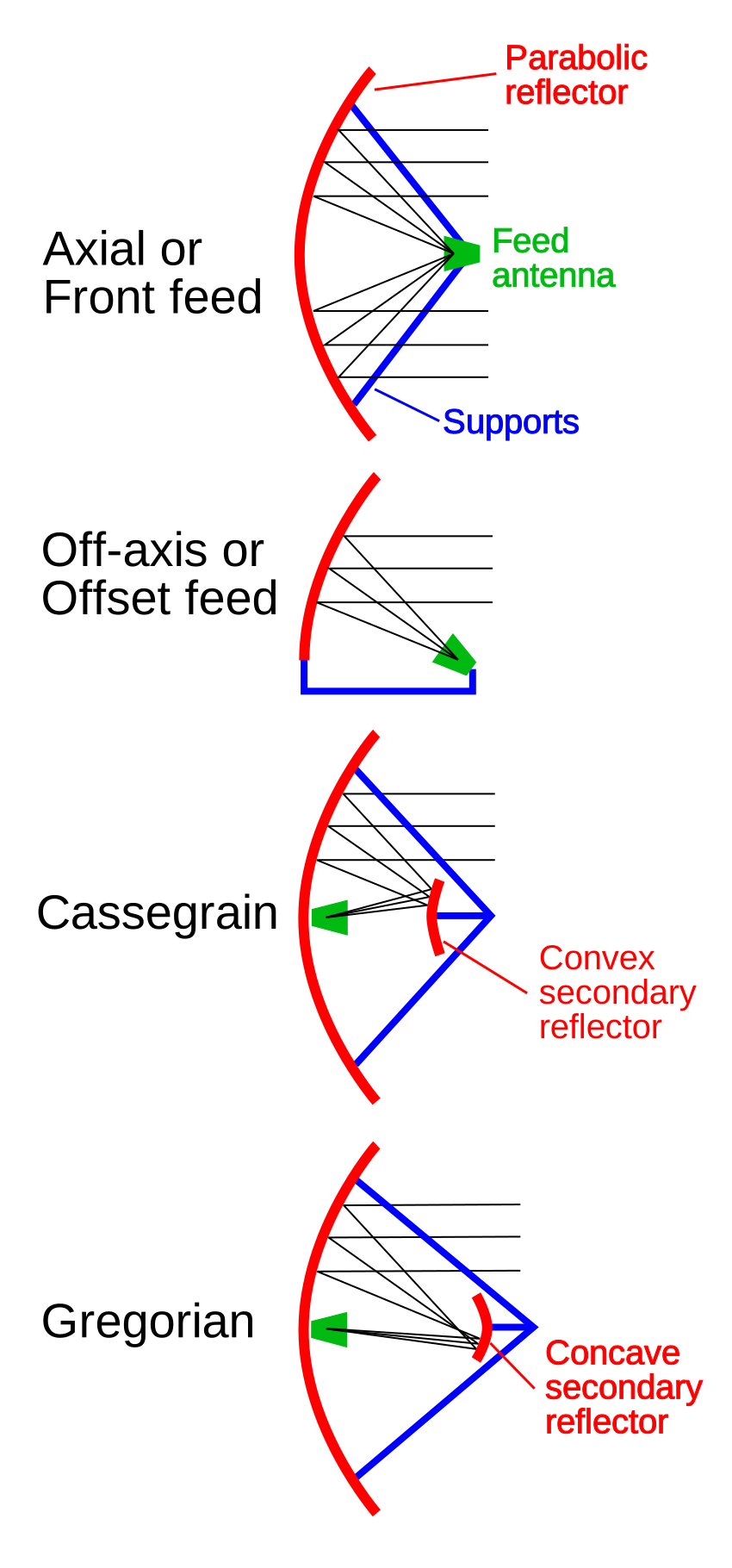
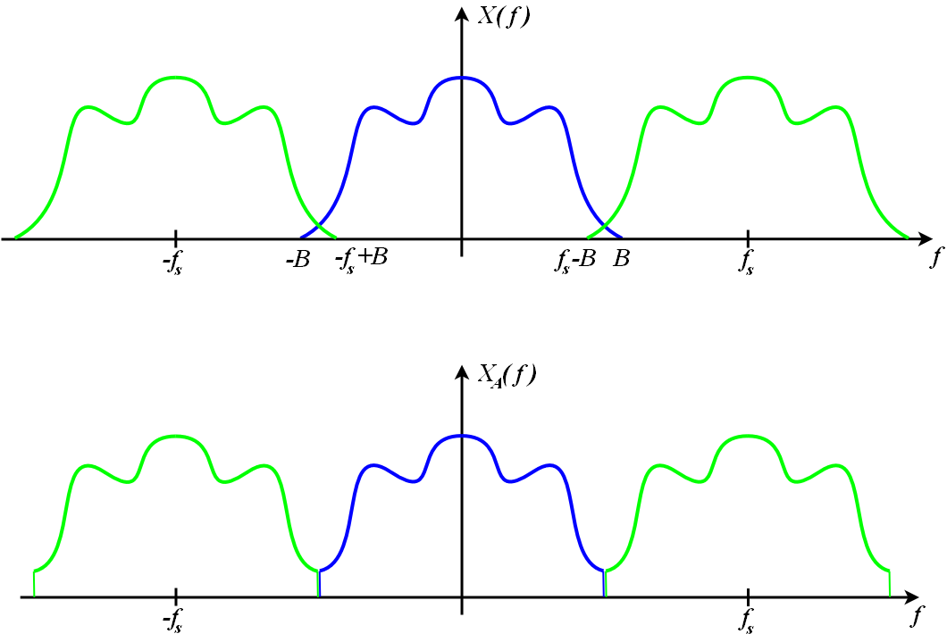
Chapter 9 Appendix
Appendix 9.A The internal signals of a TIADC
Appendix 9.B Mismatches
Appendix 9.C Impact of calibration
Appendix 9.D Time stability
Appendix 9.E Temperature stability
Appendix 9.F Stability over power cycles
Appendix 9.G Impact of Interpolation
Appendix 9.H Power consumption
Glossary
- ADC-Core
- single of a
- balun
- A special transformer to convert a symmetric signal into an asymmetric signal and vice-versa
- BRAM
- RAM integrated in ; storage location for larger datasets
- CCD
- A charge-coupled device, which is typically a 2-dimensional array of light sensitive sensors
- Cooper pair
- A weekly bound pair of electrons, which are responsible for super conductivity
- DSP-Slice
- An integrated unit in to perform fast arithmetic operations
- Fourier transform
- A Fourier transform converts functions between the time domain and the frequency domain.
- Fraunhofer lines
- A number of strong absorption lines in the optical solar spectrum
- frequency sampling method
- A method for designing with a given frequency behavior (see chapter 6.7 of\penalty\ \cite[cite]{[\@@bibref{}{DSP}{}{}]})
- gateware
- A file, which describes the configuration of an
- IF-Hybrid
- Splits an signal into two signals of equal power with a phase shift between the two signals (typically $90\text{\,}\mathrm{\SIUnitSymbolDegree}$)
- Mirror Suppression
- The ratio between the signal power and the power in mirror bands
Acronyms
- 2SB
- two-single-sideband
- ADC
- analog digital converter
- APEX
- Atacama Pathfinder Experiment
- ASIC
- application specific integrated circuit
- CCAT-prime
- Cerro Chajnantor Atacama Telescope-prime
- CHAI
- CCAT-prime Heterodyne Array Instrument
- CMOS
- complementary metal-oxide-semiconductor
- CPU
- central processing unit
- DAC
- digital analog converter
- DFT
- discrete Fourier transform
- DSP
- digital signal processing
- FF
- flip-flop
- FFT
- fast Fourier transform
- FFTS
- fast Fourier transform spectrometer
- FIR-Filter
- finite impulse response filter
- FPGA
- field programmable gate array
- HDL
- hardware description language
- IC
- integrated circuit
- IF
- intermediate frequency
- IFFT
- inverse fast Fourier transform
- IIR-Filter
- infinite impulse response filter
- LO
- local oscillator
- LUT
- look-up table
- MKID
- microwave kinetic inductance detector
- MPIfR
- Max-Planck-Institut f\"{u}r Radioastronomie
- RF
- radio frequency
- RFI
- radio frequency interference
- S/H-stage
- sample and hold stage
- SNR
- signal/noise ratio
- SSB
- single-sideband
- TIADC
- time interleaved ADC
- VHDL
- very high speed integrated circuit hardware description language