Ultra-efficient DC-gated all-optical graphene switch
Abstract
The ultrafast response and broadband absorption of all-optical graphene switches are highly desirable features for on-chip photonic switching. However, because graphene is an atomically thin material, its absorption of guided optical modes is relatively low, resulting in high saturation thresholds and switching energies for these devices. To boost the absorption of graphene, we present a practical design of an electrically-biased all-optical graphene switch that is integrated into silicon slot waveguides, which strongly confine the optical mode in the slotted region and enhance its interaction with graphene. Moreover, the design incorporates a silicon slab layer and a hafnia dielectric layer to electrically tune the saturation threshold and the switching energy of the device by applying DC voltages of <0.5 V. Using this device, a high extinction ratio (ER) of 10.3 dB, a low insertion loss (IL) of 0.7 dB, and an ultra-efficient switching energy of 79 fJ/bit at 0.23 V bias are attainable for a 40 µm long switch. The reported performance metrics for this device are highly promising and are expected to serve the needs of next-generation photonic computing systems.
August 2017
Keywords: Graphene, 2D materials, all-optical, photonic devices, switches, modulators
1 Introduction
All-optical switches are devices that control the propagation of light in a photonic data link by applying a time-varying optical signal. These devices exhibit ultrafast switching times (ps) [1], and are thus utilized for optical information processing applications in data centers, high-performance computers, and optical networks. Nevertheless, there exists an energy-speed tradeoff, where switches with a ps switching time operate at switching energies in the range of several picojoules, and sub-pJ switches operate with >1 ps switching times [2, 3]. Recently, however, an energy-efficient (35 fJ) and ultrafast (260 fs) all-optical plasmonic graphene switch was demonstrated [2]. The use of plasmonic nanostructures improves the efficiency of these devices, but they also introduce an excessive insertion loss. Next-generation telecom and datacom networks require low-energy (pJ/bit) and low-insertion-loss (dB) photonic devices [4], which necessitates the quest for designing devices with alternative structures that satisfy these requirements. It was recently reported that the switching threshold of an all-optical graphene switch can be significantly reduced by applying a few volts bias [5]. Using this method, the chemical potential of graphene is electrostatically increased by the applied DC voltage, which enables a low-energy optical pump signal to fill the remaining conduction band states and saturate the absorption of graphene, hence achieving efficient all-optical switching. Electrical control of the saturable absorption threshold in graphene was experimentally reported in [6]. In [5], the studied devices consisted of silicon nitride (Si3N4) wire waveguides, which have a relatively large cross-section and low confinement of guided light. Thus, instead of Si3N4 waveguides, we herein propose a novel design of an electrically-biased all-optical graphene switch that is integrated into silicon slot waveguides. Si slot waveguides confine and guide the optical mode in a relatively small cross-section, which strongly enhances its interaction with graphene. While several designs of all-optical graphene switches have been proposed in the literature [2, 3, 5, 7], these designs either suffer from high switching thresholds or a high insertion loss, and therefore do not meet the stringent demands of next-generation telecom and datacom networks. To overcome this challenge, we first boost the optical absorption of the graphene switch by integrating it into Si slot waveguides, where the guided optical mode is strongly enhanced and confined. Secondly, electrostatic gating is introduced into this configuration to tune the chemical potential, and thereby reduce the effective saturable absorption threshold of graphene. Because of the excellent absorption enhancement and the minimised saturable absorption threshold in this configuration, an ultra-low switching energy of 79 fJ at an applied DC voltage of 0.23 V is achieved for a 40 µm long all-optical switch, with a high extinction ratio () of 10.3 dB and a low insertion loss () of dB. These features, combined with the ultrafast response of graphene within a timescale of fs [8], are highly desirable for high-speed all-optical signal processing.
In the next section, the design methodology of the device and its structure are presented, and the modeling parameters for reproducing the results are provided. Following that, the device performance metrics are assessed by investigating its switching threshold, extinction ratio, insertion loss, and switching time. Then, these metrics are discussed and compared with those of other graphene-based devices that have been recently reported in the literature. Finally, the main findings of this report are summarized in a brief conclusion.
2 Methods
2.1 Design
The structure of the on-chip switch is illustrated in figure 1. It consists of a Si slot waveguide that is placed on top of a 10 nm thick Si slab layer, which in turn sits atop a 2 µm thick buried oxide (BOX) layer. The Si rails are 240 nm thick, resulting in a 250 nm total thickness of the Si layers. Silicon-on-insulator (SOI) substrates with 250 nm thickness are commercially available. The device dimensions are optimized to achieve a high extinction ratio and energy-efficient switching at a compact footprint. The simulated ranges and optimal dimensions of the device are given in Table 1. Hafnia is an electrical insulator with a high dielectric constant () [9], making it a useful material for building field-effect transistors [10], memristors [11], and optical modulators [12]. Thus, a 10 nm thick hafnia layer is employed to form a capacitor configuration between graphene and Si. The waveguide supports a transverse-electric (TE) mode that has a computed propagation loss of dB/µm at nm and nm (see figure 2a). The propagation loss of the TE-mode is maximized when there is no Si slab, and it reduces when the slab thickness () increases. In this design, the Si slab is essential to bias graphene with , so a minimum thickness of nm is chosen because it yields the highest absorption for the TE-mode. 80 nm Si slot waveguides can be realized in practice [13], and can achieve a high graphene absorption in our configuration (see Appendix A). The computed TE-mode is shown in the inset of figure 2a. The transverse-magnetic (TM) mode has a lower propagation loss of dB/µm at nm and nm. The higher propagation loss of the TE-mode is explained by its stronger enhancement of the electric field profile [14], which boosts the effective absorption of graphene. As explained later, the switching mechanism of the device is based on the saturable absorption of graphene. Thus, a higher absorption is desirable to obtain higher switching efficiencies, which makes the TE-mode the favorable choice. The computed values for the TE-mode at other wavelengths are presented in figure 2b. The waveguide modes are computed in Lumerical MODE, where these values are obtained for graphene and hafnia layers with a total width of µm, which is the effective absorbing width of graphene (see Appendix B).
| Parameter | ||||||||||
| Range (µm) | ||||||||||
| Optimum (µm) | 0.24 | 0.01 | 0.01 | 0.08 | 0.25 | 0.4 | 0.06 | 0.03 | 40 | 8 |


60 nm thick and 300 nm wide Au/Cr contacts supply the direct-current (DC) gate voltage () for tuning the carrier density of graphene, and the all-optical saturation threshold of graphene is electrically tuned as a result. The applied merely tunes the switching energy of the device, without switching the state of the propagating modes. Hence, the switching functionality of this device is all-optical, as explained in the next section. Moreover, the capacitor configuration that is presented in Fig. 1a, functions as an open circuit because the applied voltage is DC. As a result, the current () is zero, and thus the consumed electrical power () is zero based on [5]. As explained in Appendix C, the left and right Au/Cr contacts are placed 0.8 µm away from the left and right Si rails, respectively, to ensure that they do not induce an ohmic loss. The computed propagation loss with the Au/Cr contacts at this separation distance is exactly the same as it is without their presence, which confirms that the Au/Cr films do not contribute to the propagation loss. To obtain a high switching efficiency at a compact footprint, we set the switch length () to 40 µm. The slot waveguide is tapered to efficiently couple its guided mode with 250 nm thick silicon wire waveguides, as illustrated in figure 1b. The taper design methodology is reported in [15]. The tapered structure is simulated using the EigenMode Expansion (EME) Solver in Lumerical MODE, as shown in the inset of figure 2b. Simulations were conducted using the 3D solver with metal boundary conditions. The computed coupling efficiency and propagation loss as a function of wavelength are shown in figure 2b. High coupling efficiencies are obtained by tapering the waveguide structure, where the coupling efficiency () at nm is as high as . This result is in agreement with the one reported in [15], where a % coupling efficiency has been demonstrated for an 8 µm long taper. The % difference in our result is due to the presence of the hafnia and graphene layers, which introduce a slight mode mismatch, as confirmed by the power overlap analysis in Lumerical MODE.
2.2 Modeling parameters
The refractive index data of hBN are available in [16]. In Lumerical, graphene is simulated using the 2D model with a surface optical conductivity () [17, 18]:
| (1a) |
| (1b) |
| (1c) |
| (1d) |
where and account for the surface optical conductivity due to intraband and interband absorption, respectively. is the scattering rate of graphene, is the angular frequency of incident photons, is the electron charge, is the operation temperature, is the reduced Planck constant, is the Boltzmann constant, and is the Fermi-Dirac distribution. The refractive index data of hafnia are taken from [19]. In the optical simulation, the Au/Cr contact is simulated as a pure Au contact because the plasmonic response of Au is strong in the near-infrared (near-IR) wavelength band. The refractive index of Au are taken from [20].
3 Results
3.1 Switching energy

The absorption of graphene is tuned by Pauli-blocking [3], where photogenerated electrons fill the conduction band states of graphene following a sufficiently intense pump excitation, and by that, they block the interband transition of other electrons (see Fig. 3). At near-IR wavelengths, interband absorption is the dominant absorption mechanism in graphene [21]. The interband absorption of graphene saturates when the chemical potential () reaches a value of , as inferred from Fig. 3. Consequently, incoming pump photons cannot induce interband absorption in graphene because [21], and are therefore transmitted. Likewise, a probe photon that has an energy is also transmitted because . Making use of the Pauli-blocking physics in graphene enables all-optical switching: a probe signal is transmitted when the pump signal is ON, or absorbed when the pump signal is OFF. The interband absorption is saturated when the carrier density () of graphene increases by [3]:
| (1b) |
with being the Fermi velocity. Considering a graphene sheet with an area of , the number of electrons that would be needed to reach is . The saturation threshold or the switching energy () can be expressed as [2, 22]:
| (1c) |
In practice, there are other loss mechanisms that influence the saturation threshold of the device. Hence, the effective switching energy () is calculated by taking these loss mechanisms into account [3, 23]:
| (1d) |

with being the coupling loss, is the percentage of light absorbed by graphene, which consists of saturable and non-saturable parts, i.e. . is the non-saturable absorption percentage of [24, 25, 26], which can be taken as 5% for monolayer graphene [3, 25]. is the fraction of light that is lost due to the waveguide losses that are not related to graphene, with dB/cm taken from the values reported in [13], where a silicon slot waveguide with an 80 nm wide slot is reported. The calculated is shown in figure 4 as a function of for nm. As explained in [3], at low chemical potentials, more electrons would be needed to fill the conduction band states up to , which results in higher . Tuning the chemical potential of graphene is possible by electrostatic doping, which is achieved in our configuration by applying the gate voltage () as shown in figure 1a. Then, the relation between and µ is given by [5]:
| (1e) |
with being the effective capacitance per unit area. Figure 5a presents the equivalent capacitance of the device, and the equivalent effective capacitance is shown in the inset of figure 5b. In our configuration, , where is the hafnia capacitance, is the the capacitance of hafnia on the slot sides, and is the air capacitance. From figure 1a, nm, nm, and nm. and are the dielectric constants of air and hafnia [9], respectively. In figure 5b, it is observed that large variations in µ are obtained by applying small bias voltages of V. This is because of the high dielectric constant () and small thickness (nm) of the hafnia layer, which results in a high total effective capacitance, leading to a low . Using equation 1e, is plotted in figure 4 as a function of for nm, with being the gate voltage for the chemical potential to be tuned at the Dirac point [21]. is reduced as increases, which confirms that the switching energy of the all-optical switch is tuned by electrostatic doping of graphene. As explained in [5], this technique is not omnipotent because the non-zero scattering rate of graphene and the ambient operating temperature fundamentally limit the graphene absorption, and consequently the switching efficiency, at high bias voltages (see Supplement 1, Section 3). To operate the device without compromising its switching efficiency at nm and at an operating temperature of 300 K and a 100 fs scattering time, the maximum can correspond to a µ value of eV or less. From figure 5b, it can be seen that for , . Thus, the minimum attainable is fJ at V, based on the data presented in figure 4. Therefore, ultra-efficient all-optical switching is achieved.
3.2 Switching efficiency
The switching efficiency of the device is characterized by the extinction ratio, , and the losses are quantified by the insertion loss, [3]. and represent the transmitted power of the probe signal when the pump signal is turned off and on, respectively. The absorption of graphene is maximized when the pump signal is turned off, whereas the maximum transmission of the probe signal () is attained when a pump signal with an energy is applied. and can be expressed as [3]:
| (1f) |
| (1g) |
Using this device, a high of 10.3 dB and an ultra-low of 0.58 dB are obtained at nm. The broadband response of the device is quantified by calculating the , , and at other wavelengths, using the computed and values from figure 2b. A similar waveguide loss of dB/cm is also used for calculations at other wavelengths. Figure 6a shows the calculated and as a function of the probe signal wavelength (). It is observed that the slightly varies at other wavelengths because of the differences in , as shown in figure 2b, and as a result, the varies according to Eqs. 1f & 1g. Similarly, the slightly varies at other wavelengths because of the variations in the coupling loss, based on the computed values in figure 2b. In the studied wavelength band, % for chemical potentials up to eV (see Supplement 1, Section 3). Hence, a similar voltage (V) is applied at the other wavelengths. Figure 6b presents the computed as a function of the pump signal wavelength () at V. increases at shorter wavelengths, which agrees with experimental observations [26]. The device efficiently operates at telecom C-band wavelengths and beyond, and that is desirable for broadband optical communication networks.


3.3 Switching performance
The switching performance is quantified by the rise and fall times of the device, which are related to the electron heating and cooling mechanisms in graphene [3, 5]. Because of the conical dispersion of graphene, the density of states fades out at the Dirac point. Therefore, near the Dirac point, electrons have a relatively low heat capacity, and when photoexcited, they instantly scatter with other electrons, thereby creating a momentary sea of hot electrons in fs [27, 28, 8]. The generated sea of hot electrons later cools down in a few picoseconds by phonon- and disorder-assisted scattering [29, 30, 31, 32]. The device switching time is quantified by first considering the electrical conductivity of graphene [33, 34, 35, 17]:
| (1h) |
where is Planck’s constant. meV is the minimum conductivity plateau, and is the minimum conductivity of graphene; the values of and are taken from [33]. The mobility of graphene () can be calculated from [36]:
| (1i) |
Using the Boltzmann transport theory, the scattering time is given by [37]:
| (1j) |
Using the previously calculated quantities, the electron cooling rate () is calculated using these equations [8, 30, 33]:
| (1ka) |
| (1kb) |
| (1kc) | ||||
where K is the operating temperature, is the density of states, is the Fermi wave vector, is the mean free path, is the electron-phonon coupling constant, is the Bloch-Grüneisen temperature, 20 eV is the deformation potential constant [29], is the mass density of graphene, and is the speed of longitudinal acoustic phonons in graphene [21]. The electron cooling time () is then taken as the inverse of .
A sea of hot electrons is created within a timescale of and fills up the conduction band states, inducing Pauli-blocking. Later, photoexcited electron cool down within a timescale of [5], enabling the interband absorption of incoming photons. Therefore, and are taken as the rise and fall times of the switch, respectively. The calculated and are fs and ps, respectively, for eV. Therefore, the exceptionally fast electron heating and cooling dynamics in graphene enable ultra-high-speed switching.
4 Discussion
Table 2 summarizes the reported performance metrics of demonstrated on-chip all-optical graphene switching devices. The device presented in [2], is based on graphene-loaded plasmonic slot waveguides. It achieves the highest modulation efficiency (0.875 dB/µm), the lowest switching energy (fJ) and the fastest cooling dynamics (260 fs), but is limited by an excessive . The non-plasmonic devices that were reported in [38, 7, 39], have a much lower and can achieve high modulation efficiencies at large , but their switching energies may exceed pJ/bit at these lengths. Though this device is longer than other devices, it achieves a relatively high modulation efficiency (0.255 dB/µm), energy-efficient switching (fJ) and ultrafast recovery (ps) at an almost negligible of 0.58 dB.
| Ref. | /m | /m | |||||
|---|---|---|---|---|---|---|---|
| [2] | 19 dB | 3.5 dB | 4 µm | 0.875 dB/µm | 4.75 dB/µm | 260 fs | 35 fJ |
| [40] | n/a | 2.1 dB | 10 µm | 0.21 dB/µm | n/a | n/a | n/a a |
| [38] | negligible | 2.75 dB | 100 µm | 0.0275 dB/µm | negligible | n/a | n/a b |
| [7] | negligible | 1.1 dB c | 30 µm | 0.0367 dB/µm | negligible | 1.2 ps d | 1.38 pJ e |
| [39] | dB f | 11 dB | 288 µm g | 0.038 dB/µm | 0.0035 dB/µm | 1.29 µs | n/a h |
| Here | dB | 10.3 dB | 40 µm | 0.2575 dB/µm | dB/µm | ps | fJ |
a 46 mW is the maximum input light power; b 60 mW is the input light power; c Modulation depth is 22.7%; d Setup-limited by the resolution time of the asynchronous pump–probe system; e Saturation threshold; f Waveguide loss before transferring graphene. g Length of the graphene coating on the waveguide. h 90– 109.6 mW switching power. n/a: not available (not reported).
5 Conclusion
To sum up, we present a novel design of an all-optical graphene switch that is integrated into silicon slot waveguides, which enhance the absorption of graphene by their strong confinement of the guided optical mode. In addition, the device is electrically biased to control its saturable absorption threshold and switching energy, leading to ultra-efficient operation. Simulations were performed to optimize the design and to model the device response. Then, the device switching energy, switching efficiency, broadband response, and switching performance were discussed and compared with recently reported devices. The ultrafast response, high extinction ratio, ultra-low insertion loss and energy-efficient switching of this device are highly promising for all-optical signal processing systems.
Data availability statement
The data that support the findings of this study are available upon reasonable request from the authors.
Acknowledgments
This work was supported by the Australian Research Council (DP200101353).
Appendix A. Slot width
The slot width () is swept from 40 nm to 120 nm, and the simulated propagation losses () of the transverse-electric (TE) and transverse-magnetic (TM) modes are recorded (see figure 7). It is observed that waveguides with slot widths of 80 nm and nm yield the highest absorption. In [13], a Si slot waveguide with a slot width of nm has been demonstrated with a low propagation loss of dB/cm. Thus, our device is designed with a similar slot width.

Appendix B. Effective absorbing width
Initial simulations were performed with a 3.48 µm wide graphene sheet as shown in figure 1. The resulting propagation loss () for the TE-mode is dB/µm. It might be assumed that the portion of graphene that is on top of the slotted region is the one that solely contributes to the absorption of the waveguide mode, because that is where the waveguide mode is mostly confined. However, when simulating the same structure with an 80 nm wide graphene sheet on top of the slotted region, as shown in figure 2, the resulting is merely dB/µm. This indicates that other portions of the graphene sheet significantly contribute to the absorption. Therefore, the width of the graphene sheet is swept to find out the effective absorbing width, which would yield a dB/µm propagation loss. It is found out that a 1.64 µm wide graphene sheet yields a dB/µm propagation loss (see figure 3). Hence, 1.64 µm is taken as the effective absorbing width for calculating the switching energy.


Appendix C. Contact spacing
To ensure that the Au/Cr does not induce an ohmic loss, the distance between the metal contacts and Si ralis, denoted by , is swept from 0 to 0.8 µm, and the propagation loss () is recorded. It is noted that reaches a plateau at large , which indicates that the metal contacts are far from the guided mode and cannot induce ohmic losses. A contact spacing of 0.8 nm is chosen because the ohmic losses are eliminated at this distance.

Appendix D. Graphene absorption
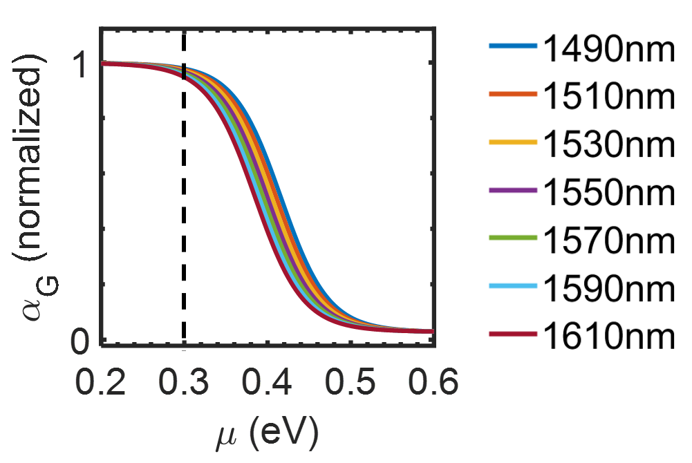
As mentioned in the main text, the absorption of graphene abruptly falls for eV, because of the non-zero scattering rate and the ambient operating temperature (see figure 1). As explained in [5], can correspond to a µ value of eV or less, to operate the device with a high switching efficiency. The maximum transmittance () in the ON state is , as given in the main text. A reduced graphene absorption () reduces , which in turn reduces the maximum extinction ratio (), where , as given in the main text. In figure 1, it is observed that the absorption falls abruptly for eV, for all wavelengths in the studied band. Figure 1 is plotted for a temperature of 300 K and 100 fs scattering time, following the steps given in [5].
References
References
- [1] Chai Z, Hu X, Wang F, Niu X, Xie J and Gong Q 2017 Advanced Optical Materials 5 1600665
- [2] Ono M, Hata M, Tsunekawa M, Nozaki K, Sumikura H, Chiba H and Notomi M 2020 Nature Photonics 14 37–43
- [3] Alaloul M and Rasras M 2021 ACS Omega
- [4] Giambra M A, Miseikis V, Pezzini S, Marconi S, Montanaro A, Fabbri F, Sorianello V, Ferrari A C, Coletti C and Romagnoli M 2021 ACS nano 15 3171–3187
- [5] Alaloul M and Khurgin J B 2022 Optics Express 30 1950–1966
- [6] Alexander K, Hu Y, Pantouvaki M, Brems S, Asselberghs I, Gorza S P, Huyghebaert C, Van Campenhout J, Kuyken B and Van Thourhout D 2015 Electrically controllable saturable absorption in hybrid graphene-silicon waveguides CLEO: Science and Innovations (Optical Society of America) pp STh4H–7
- [7] Wang H, Yang N, Chang L, Zhou C, Li S, Deng M, Li Z, Liu Q, Zhang C, Li Z et al. 2020 Photonics Research 8 468–474
- [8] Alaloul M and Rasras M 2021 JOSA B 38 602–610
- [9] Robertson J 2004 The European physical journal applied physics 28 265–291
- [10] Mikolajick T, Müller S, Schenk T, Yurchuk E, Slesazeck S, Schröder U, Flachowsky S, van Bentum R, Kolodinski S, Polakowski P et al. 2014 Advances in Science and Technology 95 136–145
- [11] Chen P Y, He Z Y, Cha M Y, Liu H, Zhu H, Chen L, Sun Q Q, Ding S J and Zhang D W 2021 physica status solidi (a) 218 2000635
- [12] Bonando M G, Araújo M C and Saito L A 2018 All-fiber graphene electro-optic modulators with different dielectric materials 2018 SBFoton International Optics and Photonics Conference (SBFoton IOPC) (IEEE) pp 1–4
- [13] Serna S, Zhang W, Leroux X, Gao D, Zhang D, Vivien L and Cassan E 2014 JOSA B 31 2021–2028
- [14] Leuthold J, Koos C and Freude W 2010 Nature photonics 4 535–544
- [15] Wang Z, Zhu N, Tang Y, Wosinski L, Dai D and He S 2009 Optics letters 34 1498–1500
- [16] Rah Y, Jin Y, Kim S and Yu K 2019 Optics letters 44 3797–3800
- [17] Alaloul M and Khurgin J 2021 IEEE Photonics Journal
- [18] Hanson G W 2008 Journal of Applied Physics 103 064302
- [19] Al-Kuhaili M 2004 Optical Materials 27 383–387
- [20] Yakubovsky D I, Arsenin A V, Stebunov Y V, Fedyanin D Y and Volkov V S 2017 Optics express 25 25574–25587
- [21] Liu J M and Lin I T 2018 Graphene photonics (Cambridge University Press)
- [22] Alaloul M and Khurgin J B 2022 IEEE Journal of Selected Topics in Quantum Electronics 28 1–8
- [23] Alaloul M, Khurgin J B, Al-Ani I, As’ham K, Huang L, Hattori H T and Miroshnichenko A E 2022 Optics Letters 47 3640–3643
- [24] Bao Q, Zhang H, Wang Y, Ni Z, Yan Y, Shen Z X, Loh K P and Tang D Y 2009 Advanced Functional Materials 19 3077–3083
- [25] Bao Q, Zhang H, Ni Z, Wang Y, Polavarapu L, Shen Z, Xu Q H, Tang D and Loh K P 2011 Nano Research 4 297–307
- [26] Zhang F, Han S, Liu Y, Wang Z and Xu X 2015 Applied Physics Letters 106 091102
- [27] Tielrooij K J, Piatkowski L, Massicotte M, Woessner A, Ma Q, Lee Y, Myhro K S, Lau C N, Jarillo-Herrero P, van Hulst N F et al. 2015 Nature nanotechnology 10 437–443
- [28] Chen Y, Li Y, Zhao Y, Zhou H and Zhu H 2019 Science advances 5 eaax9958
- [29] Song J C, Reizer M Y and Levitov L S 2012 Physical review letters 109 106602
- [30] Ma Q, Gabor N M, Andersen T I, Nair N L, Watanabe K, Taniguchi T and Jarillo-Herrero P 2014 Physical review letters 112 247401
- [31] Chen J H, Jang C, Adam S, Fuhrer M, Williams E D and Ishigami M 2008 Nature physics 4 377–381
- [32] Graham M W, Shi S F, Ralph D C, Park J and McEuen P L 2013 Nature Physics 9 103–108
- [33] Lin Y, Ma Q, Shen P C, Ilyas B, Bie Y, Liao A, Ergeçen E, Han B, Mao N, Zhang X et al. 2019 Science advances 5 eaav1493
- [34] Song J C, Rudner M S, Marcus C M and Levitov L S 2011 Nano letters 11 4688–4692
- [35] Shiue R J, Gao Y, Wang Y, Peng C, Robertson A D, Efetov D K, Assefa S, Koppens F H, Hone J and Englund D 2015 Nano letters 15 7288–7293
- [36] Yan J and Fuhrer M S 2011 Physical review letters 107 206601
- [37] Zhu W, Perebeinos V, Freitag M and Avouris P 2009 Physical Review B 80 235402
- [38] Sun F, Xia L, Nie C, Shen J, Zou Y, Cheng G, Wu H, Zhang Y, Wei D, Yin S et al. 2018 Nanotechnology 29 135201
- [39] Qiu C, Zhang C, Zeng H and Guo T 2021 Journal of Lightwave Technology 39 2099–2105
- [40] Sun F, Xia L, Nie C, Qiu C, Tang L, Shen J, Sun T, Yu L, Wu P, Yin S et al. 2019 Applied Physics Express 12 042009