Reversible canted persistent spin textures in two-dimensional ferroelectric bilayer WTe2
Abstract
The recent discovery of materials hosting persistent spin texture (PST) opens an avenue for the realization of energy-saving spintronics since they support an extraordinarily long spin lifetime. However, the stability of the PST is sensitively affected by symmetry breaking of the crystal induced by external perturbation such as the electric field. In this paper, through first-principles calculations supplemented by symmetry analysis, we report the emergence of the robust and stable PST with large spin splitting in the two-dimensional (2D) ferroelectric bilayer WTe2. Due to the low symmetry of the crystal ( point group), we observe a canted PST in the spin-split bands around the Fermi level displaying a unidirectional spin configuration tilted along the plane in the first Brillouin zone. Such a typical PST can be effectively reversed by out-of-plane ferroelectric switching induced by interlayer sliding along the in-plane direction. We further demonstrated that the reversible PST is realized by the application of an out-of-plane external electric field. Thus, our findings uncover the possibility of an electrically tunable PST in 2D materials, offering a promising platform for highly efficient and non-volatile spintronic devices.
Keywords:
Suggested keywordspacs
Valid PACS appear hereI INTRODUCTION
The next generation of spintronics relies on the effective control and manipulation of an electron’s spin degree of freedom without an additional external magnetic field, which is achievable by utilizing the effect of spin-orbit coupling (SOC)Manchon et al. 2015. Many intriguing SOC-related phenomena were discovered, including spin relaxation Fabian and Sarma 1999; Averkiev and Golub 1999, spin Hall effect Qi, Wu, and Zhang 2006, spin galvanic effect Ganichev et al. 2002, and spin ballistic transport Lu et al. 1998. In non-magnetic systems lacking inversion symmetry, the SOC induces momentum -dependent spin-orbit field (SOF) that lifts Kramer’s spin degeneracy and results in chiral spin polarization characterized by the spin-momentum-locking property as manifested by the Dresselhaus Dresselhaus 1955 and Rashba Rashba 1960 effects. The Dresselhaus effect is generally observed on a system holding bulk inversion asymmetries such as bulk zinc blende Dresselhaus 1955 and wurtzite Wang et al. 2007 semiconductors. On the other hand, the Rashba effect is associated with heterostructures and surfaces due to two-dimensional (2D) structural inversion asymmetry, as widely observed on semiconductor quantum-well (QW) Nitta et al. 1997; Caviglia et al. 2010, surface heavy metal LaShell, McDougall, and Jensen 1996; Koroteev et al. 2004, and several 2D-layered compounds Zhuang et al. 2015; Popović, Kurdestany, and Satpathy 2015; Absor et al. 2018a; Affandi and Ulil Absor 2019; Absor et al. 2017a.
Recently, ferroelectric Rashba materials (FRMs) have stimulated the interest of researchers due to the reversible spontaneous polarization and the inherent Rashba effect Picozzi 2014; Wang et al. 2020; Varotto et al. 2021. Here, reversible Rashba spin textures can be achieved in a non-volatile way by switching the direction of the ferroelectric polarization Picozzi 2014, which is promising for electrically controllable spintronic devices Matos-Abiague and Fabian 2015; Wang et al. 2020; Varotto et al. 2021. -GeTe was the first FRM predicted Di Sante et al. 2012, and its reversible spin texture by switching ferroelectric polarization has been experimentally confirmed Liebmann et al. 2016; Rinaldi et al. 2018. After that, a handful of ferroelectric materials ranging from similar metal chalcogenides (SnTe) to metal-organic halide perovskites, such as (FA)SnI3 Stroppa et al. 2014, hexagonal semiconductors (LiZnSb) Narayan 2015, and perovskite oxides (HfO2 Tao et al. 2017, and BiAlO3 da Silveira, Barone, and Picozzi 2016, were proposed to be FRMs. Despite the robust ferroelectricity, the strong SOC in these materials makes them promising for the realization of FRM-based spintronics devices. However, the strong SOC may induce fast spin decoherence through the Dyakonov-Perel (DP) spin relaxation mechanism Dyakonov and Perel 1972, reducing spin lifetime, and hence limiting the performance of potential spintronic devices.
A possible way to circumstance this obstacle is to engineer a structure where the SOF orientation is momentum-independent. In a such condition, the spin configuration in the momentum space becomes unidirectional, leading to the well-known persistent spin texture (PST) as was firstly proposed by Schliemann et al. Schliemann, Egues, and Loss 2003. The PST enables a route to overcome spin dephasing and provides non-dissipative spin transport Bernevig, Orenstein, and Zhang 2006; Altmann et al. 2014, thus holding great promise for future spintronic applications. Previously, the PST has been demonstrated on semiconductor quantum-well (QW) having equal strength to the Dresselhaus and Rashba SOC Bernevig, Orenstein, and Zhang 2006; Walser et al. 2012; Sasaki et al. 2014 or on [110]-oriented semiconductor QWs in which the SOC is described by the [110] Dresselhaus model Bernevig, Orenstein, and Zhang 2006. Recently, a more robust PST has been proposed imposing the symmetry of the crystal as reported on bulk BiInO3 ( space group) Tao and Tsymbal 2018. The symmetry-protected PST with purely cubic spin splitting has also been recently reported in bulk materials crystallizing in the and point groups Zhao et al. 2020. Furthermore, the canted PST driven by the lower symmetry of the crystal has also been reported on ZnO (100) surface Absor et al. 2015 and monolayer transition metal dichalcogenides (TMDCs) including monolayers WTe2 Garcia et al. 2020 and MoTe2 Vila et al. 2021.
Despite these advances, 2D ferroelectric materials with in-plane electric polarization have also been proposed to support the PST Ai et al. 2019; Absor et al. 2021; Absor and Ishii 2019a; Anshory and Absor 2020; Absor and Ishii 2019b; Lee, Im, and Jin 2020; Sasmito et al. 2021; Absor and Ishii 2021; Jia et al. 2020. Here, the SOC leads to the unidirectional out-of-plane SOF, resulting in the PST with a unidirectional out-of-plane spin configuration. Various 2D ferroelectric materials including WO2Cl2 Ai et al. 2019, Ga(=Se, Te; =Cl, Br, I) Sasmito et al. 2021; Absor and Ishii 2021, hybrid perovskite benzyl ammonium lead-halide Jia et al. 2020, and group-IV monochalcogenide Absor et al. 2021; Absor and Ishii 2019a; Anshory and Absor 2020; Absor and Ishii 2019b; Lee, Im, and Jin 2020, has been reported to exhibit the PST. However, considering the nature of the in-plane ferroelectricity in these 2D materials, the presence of the PST can be destroyed by disturbing the in-plane ferroelectricity, for an instant, through the application of an external out-of-plane electric field Sławińska et al. 2020; Absor et al. 2021, thus hindering their practical spintronics. Therefore, finding novel 2D ferroelectric materials with robust and stable PST under the external electric field is highly desirable for practical purposes.
In this paper, through first-principles density-functional theory (DFT) calculations, we report the emergence of robust and stable PST in the 2D ferroelectric bilayer WTe2. Recently, it has been reported that the bilayer WTe2 is semimetal exhibiting interlayer sliding ferroelectricity Fei et al. 2018; Sharma et al. 2019; Wang and Qian 2019; Liu et al. 2019a; Yang, Wu, and Li 2018, thus achieving the stable PST is expected to be useful for non-volatile spintronics. We find that a unidirectional spin configuration is observed in the spin-split bands around the Fermi level, which is tilted along the plane in the first Brillouin zone (FBZ), forming a canted PST. Such a peculiar PST is strongly different from the well-known PST discovered on semiconductor QW Bernevig, Orenstein, and Zhang 2006; Walser et al. 2012; Sasaki et al. 2014, bulk systems Tao and Tsymbal 2018; Zhao et al. 2020, and various 2D ferroelectric materials Ai et al. 2019; Absor et al. 2021; Absor and Ishii 2019a; Anshory and Absor 2020; Absor and Ishii 2019b; Lee, Im, and Jin 2020; Sasmito et al. 2021; Absor and Ishii 2021; Jia et al. 2020. Our -based symmetry analysis clarified that the observed canted PST in the present systems is enforced by the out-of-plane mirror symmetry of the point group. More importantly, we found that the orientation of the canted PST can be effectively reversed upon ferroelectric switching, which is demonstrated through the application of an out-of-plane external electric field. This reversible canted PST, which is not found in the previously reported canted PST on the monolayer TMDCs such as monolayers WTe2 Garcia et al. 2020 and MoTe2 Vila et al. 2021, is promising for non-volatile and efficient spintronic applications.
II Computational details
We have performed first-principles DFT calculations based on norm-conserving pseudo-potentials and optimized pseudo-atomic localized basis functions implemented in the OpenMX code Ozaki 2003; Ozaki and Kino 2005; Ozaki and Kino 2005. The exchange-correlation functional was treated within generalized gradient approximation by Perdew, Burke, and Ernzerhof (GGA-PBE) Perdew, Burke, and Ernzerhof 1996; Kohn and Sham 1965. The basis functions were expanded by a linear combination of multiple pseudo atomic orbitals (PAOs) generated using a confinement scheme Ozaki 2003; Ozaki and Kino 2004, where three -, three -, two -character numerical PAOs were used. The accuracy of the basis functions, as well as pseudo-potentials we used, were carefully bench-marked by the delta gauge method Lejaeghere et al. 2016.
We used a periodic slab to model the bilayer WTe2, where a sufficiently large vacuum layer (25 Å) was applied to avoid the spurious interaction between slabs. We used a -point and real space grids corresponding to energy cutoffs larger than 300 Ry to obtain the converged results of the self-consistent field (SCF) loops. The minimum-energy pathways of ferroelectric transitions were evaluated by using nudged elastic band (NEB) method based on the interatomic forces and total energy calculations Henkelman and Jónsson 2000. We adopted the modern theory of polarization based on the Berry phase (BP) method King-Smith and Vanderbilt 1993 to calculate the ferroelectric polarization. We considered a uniform external electric field perpendicular to the 2D plane of the crystal modeled by a sawtooth waveform during the SCF calculation and geometry optimization. Here, the energy convergence criterion was set to eV. The lattice and positions of the atoms were optimized until the Hellmann-Feynman force components acting on each atom were less than 1 meV/Å.
To evaluate the spin-splitting-related properties, we perfomed non-collinear DFT calculations, where the SOC was included self consistently in all calculations by using -dependent pseudo potentials (Theurich and Hill 2001). We calculated the spin textures by deducing the spin vector components (, , ) in the reciprocal lattice vector from the spin density matrix. Here, by using the spinor Bloch wave function, , obtained from the OpenMX calculations after the SCF is achieved, we calculate the spin density matrix, , through the following relation Kotaka, Ishii, and Saito 2013,
| (1) | |||
where is the overlap integral of the -th and -th localized orbitals, is expansion coefficient, () is the spin index ( or ), is the band index, and is the -th lattice vector. This method has been successfully applied in our previous studies on various 2D materials Sasmito et al. 2021; Absor and Ishii 2021; Absor et al. 2021; Absor et al. 2020; Absor and Ishii 2019a; Absor and Ishii 2019b; Absor et al. 2018b; Absor et al. 2017b

III Results and Discussion
III.1 Atomic structure, symmetry, and ferroelectricity
Figs. 1(a)-(b) show the crystal structures of monolayer and bilayer WTe2, respectively, corresponding to the FBZ [Fig. 1(c). Monolayer WTe2 is stable in the structure Hsu et al. 2020; Tang et al. 2017; Wang and Qian 2019, where the tungsten (W) atoms are octahedrally coordinated by the telluride (Te) atoms and the W atoms form a slightly buckled zigzag chain due to the metallic bonding, resulting in a distortion of the Te octahedron around each Te atom [Fig. 1(a)]. Symmetrically, monolayer WTe2 is centrosymmetric belonging to point groupHsu et al. 2020; Wang and Qian 2019 generated by the following symmetry operations: (i) identity operation , (ii) inversion symmetry , (iii) a mirror symmetry perpendicular to the axis, and (iv) a two-fold screw rotation symmetry around the axis [Fig. 1(a)]. Upon van der Walls stacking, bilayer WTe2 forms a layered orthorhombic structure known as the phase)Wang and Qian 2019, where both the inversion and screw rotation symmetries are broken [Fig. 1(b)]. Therefore, the crystal symmetry of bilayer WTe2 becomes point group Wang and Qian 2019. We find that the optimized structure of bilayer WTe2 for and lattice parameters are 3.48 Å and 6.27 Å, respectively, which are slightly different from that of monolayer WTe2 [ Å and Å]. However, these values are in good agreement with the previous theoretical reports Wang and Qian 2019; Liu et al. 2019a; Yang, Wu, and Li 2018 and experiments Fei et al. 2018; Sharma et al. 2019. Due to the substantial difference between the and parameters, the crystal geometry of the monolayer and bilayer WTe2 is strongly anisotropic, implying that these materials have a strongly anisotropic mechanical response being subjected to the uniaxial strain along the - and -direction similar to that observed on group IV monochalcogenide Anshory and Absor 2020; Kong et al. 2018; Liu et al. 2019b.
The low symmetry of the bilayer WTe2 plays an important role in generating the out-of-plane ferroelectricity. Here, the absence of both the inversion and glide in-plane mirror symmetries in bilayer WTe2 induces a small in-plane shift () between adjacent layers along the axis (known as in-plane interlayer sliding) Wang and Qian 2019; Liu et al. 2019a; Yang, Wu, and Li 2018; Fei et al. 2018; Sharma et al. 2019, where is the in-plane shift along the -direction between the upper and lower layers with respect to the inversion center as shown by the dashed red and blue lines in Fig. 1(b). In our calculation, the in-plane shift is found to be 0.51 Å, which is much smaller than that of the out-of-plane interlayer distance () of 3.19 Å, but is agree-well with the previously calculated results Wang and Qian 2019; Liu et al. 2019a; Yang, Wu, and Li 2018. Accordingly, a net charge transfer between the upper and lower layer is allowed, which is expected to produce an interface dipole in the out-of-plane direction. This is, in fact, confirmed by our calculated results of differential charge density shown in Fig. 1(d), displaying a vertical polarity induced by the electron depletion (blue color) and accumulation (red color) at the interlayer interface.
To further clarify the robustness of the out-of-plane ferroelectricity in bilayer WTe2, we show in Fig. 1(e) the calculated results of the ferroelectric transition pathways obtained from the NEB calculation. We find that two opposite ferroelectric (FE) states with the opposite orientation of the out-of-plane electric polarization () are observed, which can be reversed by the in-plane shift () between adjacent layers, passing through an intermediate paraelectric (PE) state with [see the insert of Fig. 1(e)]. The intermediate PE state in bilayer WTe2 has a point group due to an additional in-plane glide mirror symmetry operation, an in-plane mirror symmetry operation followed by a translation along by a fractional translation of , thus enforcing the vanishing of . Through BP calculation, we found that the calculated in the FE state is cm-2, which is in good agreement with the previous experimental value Fei et al. 2018; Sharma et al. 2019 and the calculated results Wang and Qian 2019; Liu et al. 2019a; Yang, Wu, and Li 2018. Moreover, the transition pathway connecting the two opposite FE states through the PE state yields barrier energy of 0.45 meV [Fig. 1(e)], which is much smaller than that observed on the well-known ferroelectric BaTiO3 Haeni et al. 2004, suggesting the feasibility of a ferroelectric switch under ambient conditions.

III.2 Electronic structure, spin splitting, and spin polarization
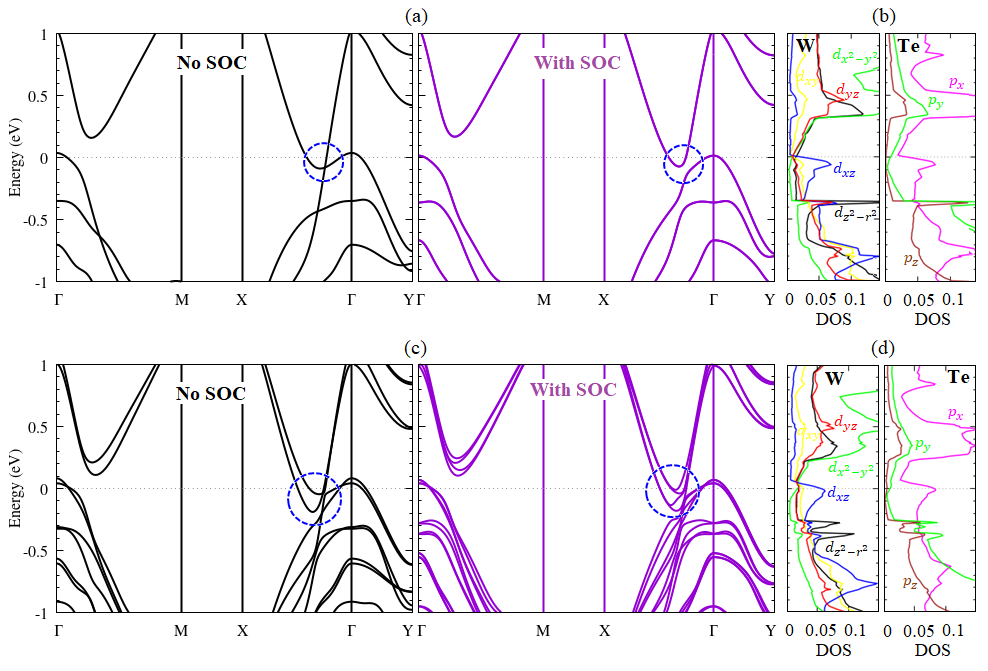
Figs. 2(a)-(c) show the electronic band structure of monolayer and bilayer WTe2, respectively, calculated along the selected path in the FBZ. One can see that both the monolayer and bilayer WTe2 show a semi-metallic character of the electronic state. In the absence of the SOC, the monolayer WTe2 exhibits band crossing between the highest occupied state (HOS) and lowest unoccupied state (LUS) at the point near the Fermi level along the line [see blue dashed lines in Fig. 2(a)], forming a Dirac nodal point Muechler et al. 2020; Ok et al. 2019; Xu et al. 2018; Qian et al. 2014, which is protected by screw rotation symmetry. Turning the SOC opens this Dirac nodal point and the monolayer WTe2 becomes a 2D topological insulator Muechler et al. 2020; Ok et al. 2019; Qian et al. 2014; Xu et al. 2018. However, due to the presence of the inversion symmetry in the monolayer WTe2, all the bands remain degenerated in the entirely FBZ [see right side of Fig. 2(a)]. Our calculated results of the density of states projected to the atomic orbitals confirmed that the states near the Fermi level (HOS and LUS) mainly originated from the strong hybridization between the W- and Te- orbitals [Fig. 2(b)].
For the case of the bilayer WTe2, on the other hand, we observe two HOS and two LUS near the Fermi level along the line [Fig. 2(c)] characterized by the strong mixing between the W- and the Te- states [Fig. 2(d)], which is similar to the HOS and LUS in the monolayer WTe2. However, there is no band crossing (Dirac nodal point) observed in the bilayer WTe2 [Fig. 2(c)], which is due to the broken of the screw rotation symmetry. In addition, due to the lack of the inversion symmetry in the bilayer WTe2, the SOC leads to the significant spin-splitting bands, which is particularly pronounced at the LUS near the Fermi level along the line [see the right side in Fig. 2(c)]. The emergence of the spin-splitting bands in the bilayer WTe2 makes them more beneficial for spintronic applications. Therefore, in the following discussion, we will focus only on the spin-splitting-related properties of the bilayer WTe2.
Figs. 3(a)-(b) show the band structure of bilayer WTe2 highlighting the two LUS along the line (labeled by the band (1) and (2)) obtained without and with the SOC, respectively. Since the LUS are close to the Fermi level, it is expected that they play a significant role in the transport properties of the carriers. By comparing Figs. 3(a) and 3(b), it is clearly seen that large spin splitting is observed at the two LUS, where the spin-splitting energy up to 0.09 eV and 0.12 eV is observed on the pair bands (1) and (2), respectively. These values are comparable to that observed on various 2D ferroelectric systems including group IV monochalcogenides (0.02 - 0.3 eV) Absor et al. 2021; Absor and Ishii 2019a; Anshory and Absor 2020; Absor and Ishii 2019b and Ga(=Se, Te; =Cl, Br, I) family (0.25 eV) Absor and Ishii 2021, which is certainly sufficient to ensure the proper function of spintronic devices operating at room temperature. By mapping the spin-splitting energy of the LUS projected to the FBZ, we observed a strongly anisotropic spin splitting, where the large spin-splitting energy emerges at the bands along the line, while very small spin-splitting energy appears at the bands along the line [Figs. 3(c)-(d)]. This anisotropic nature of the spin-splitting energy observed in the LUS is enforced by the low symmetry of the crystal that is similar to that observed on various 2D group IV monochalcogenides Absor et al. 2021; Absor and Ishii 2019a; Anshory and Absor 2020; Absor and Ishii 2019b and Ga(=Se, Te; =Cl, Br, I) family Absor and Ishii 2021.
To further characterize the spin-splitting bands at the LUS, we show the calculated result of spin-resolved projected to the bands as displayed in Fig. 4(a). Due to the presence of the mirror plane in the bilayer WTe2, the spin polarization has no -component of spin (), but exhibits a significant - and -componets of spin (, ), indicating that the spin polarizations are tilted along the plane in the FBZ. By calculating the -space spin textures for the upper and lower bands [Figs. 4(c) and 4(d), respectively] in the spin-split pair bands (1) [see Figs. 3(a)-(b)], we observe a unidirectional spin configuration that is visible at the substantially large region in the FBZ. Such a tilting and unidirectional spin configuration in the -space lead to the formation of the canted PST, which differs strongly from the widely reported PST discovered on semiconductor QW Bernevig, Orenstein, and Zhang 2006; Walser et al. 2012; Sasaki et al. 2014, bulk systems Tao and Tsymbal 2018; Zhao et al. 2020, and various 2D ferroelectric materials Ai et al. 2019; Absor et al. 2021; Absor and Ishii 2019a; Anshory and Absor 2020; Absor and Ishii 2019b; Lee, Im, and Jin 2020; Sasmito et al. 2021; Absor and Ishii 2021; Jia et al. 2020. We noted here that the canted PST has been previously reported on ZnO (100) surface Absor et al. 2015 and monolayer TMDCs such as monolayers WTe2 Garcia et al. 2020 and MoTe2 Vila et al. 2021. The observed canted PST in the present system is expected to induce unidirectional canted SOF in the -space, which protects the spin from decoherence and induces an extremely long spin lifetime Schliemann, Egues, and Loss 2003; Altmann et al. 2014; Bernevig, Orenstein, and Zhang 2006. In fact, a robust spin diffusion over long distances has been reported in few-layered MoTe2 at room temperature Song et al. 2020, offering a promising platform to realize an efficient spintronics device.

To understand the nature of the observed canted PST, we consider a symmetry-based Hamiltonian model recently used for 2D TMDCs with structure Garcia et al. 2020; Vila et al. 2021. Since the electronic states near the Fermi level around the point belongs to the IRs ( orbital) and ( orbital) of the point group, one can construct the following Hamiltonian:
| (2) |
where the first term describes the Hamiltonian without the SOC:
| (3) |
Here, () with and () are the Pauli matrices and identity matrix working in the orbital (spin) space, respectively, and is the effective mass of the occupied (unoccupied) bands. , , and are the parameter representing the degree of the crystalline anisotropy between and , the breaking of the inversion symmetry, and the degree of the band inversion, respectively. The second term in Eq. (2) represents the SOC term which can be written in the first order in as
| (4) |
where , , and are the SOC parameters. Eq. (4) is the symmetry-allowed SOCs obtained by considering the mirror symmetry and time reversal symmetry , where for the spinor and is the complex conjugation.
By focusing on the spin-split states along the line (), the following simplified Hamiltonian holds,
| (5) |
From the last two terms of Eq. (5), it is obvious that the spin textures should be unidirectionally tilted along the plane, which is agree-well with the observed spin-resolved bands shown in Fig. 4(a) and the -space spin texture presented in Figs. 4(b)-(c). Moreover, the SOC parameters (, ), which are important for spintronics device operations, can be evaluated by fitting the energy dispersion obtained from the solution of Eq. (5) to the DFT energy bands along the . For the lowest unoccupied bands [see the pair bands (1) in Fig. 3(b)], we find that the calculated SOC parameters are 0.09 eVÅ and 1.15 eVÅ for and , respectively. These values are much larger than that observed on various semiconductor QW Walser et al. 2012; Sasaki et al. 2014.
It is noted here that the observed canted PST in the spin-split bands of the LUS near the Fermi level makes them possible to be resolved by using spin-polarized angle-resolved photo-electron spectroscopy (SARPES). Recently, Fanciulli et.al successfully measure the spin polarization of electrons near the Fermi level in the bulk WTe2 by combining a SARPES measurement with a high-harmonic generation laser source Fanciulli et al. 2020. Therefore, considering the similar electronic state, resolving the canted PST in the bilayer WTe2 is plausible. Moreover, it is also feasible to observe the formation of the PST by injecting the electron in the LUS, which could be performed by using near-field scanning Kerr microscopy Rudge et al. 2015 to resolve the features down to tens-nm scale with sub-ns time resolution. Furthermore, exploration of the current-induced spin polarization driven by the Edelstein effect Edelstein 1990 and associated spin-orbit torques Gambardella and Miron 2011 is also possible in the bilayer WTe2 by applying an electron doping. Since the electron doping on the bulk WTe2 has been experimentally realized Li et al. 2022, observation of the current-induced spin polarization in the bilayer WTe2 under the electron doping is plausible, which is expected to show the better resolution due to the stronger SOC.
III.3 Reversible Canted PST
To enrich the physics and possible application of the present systems, we examine the correlation between the observed canted PST and ferroelectricity. Here, an interesting property known as reversible canted PST holds, i.e., the orientation of the unidirectional tilted spin configuration is reversed by switching the direction of the out-of-plane spontaneous electric polarization . Fig. 5 displays the evolution of the spin-resolved bands near the Fermi level along the line in the bilayer WTe2 under the different orientation of the out-of-plane ferroelectric polarization . Interestingly, when the direction of is reversed, the out-of-plane spin component () is invariant, while the in-plane spin component is reversed simultaneously [Figs. 5(a) and 5(c)]. As a result, a reversible canted PST is achieved as schematically shown in Figs. 5(b) and 5(d). Such a reversible PST offers a promising platform to realize a non-volatile control of the PST through the application of the external electric field, which is useful for spintronics devices implementing spin Hall effect Matos-Abiague and Fabian 2015; Wang et al. 2020; Varotto et al. 2021.

The physical mechanism behind the reversible canted PST can be understood in terms of symmetry analysis. Let us considered a general symmetry operator , where is point group symmetry operation and is the translation vector operator. Since the spin polarization vector is a time-reversal pseudovector, for a given symmetry operator , the can be transformed by the relation , where is the spatial (temporal) parity operator correlated with . In particular, when , where is the multiples of the reciprocal lattice vector. As for the bilayer WTe2, the reversal polarization () direction between the two FE states is related to the PE state having glide in-plane mirror symmetry [see Fig. 1(d)], thus we obtained that and . Accordingly, the reversal canted PST can also be correlated to through the following transformation: . This shows that the canted PST is reversed as the sign of the spin component is reversed, which is consistent-well with the observed spin-resolved bands and the spin textures are shown in Fig. 5.
We emphasized here that the reversible canted PST observed in the present study is the key for the nonvolatile spintronic applications. Here, the application of an electric field is an effective method to realize the reversible canted PST. Therefore, we introduce an external electric field () oriented perpendicular to the 2D surface (-direction), which can be implemented through the application of a gate voltage Sławińska et al. 2020; Absor et al. 2021. Since the reversible canted PST in bilayer WTe2 depends on the sign of the spin component [see Figs. 5(a) and 5(c)], we further show in Fig. 6(a) the modulation of the under the different sign and magnitude of the electric field . Obviously, we identify the reversible spin polarization as indicated by the reversal sign of the under the switching direction of .

By calculating the spin polarization at the certain [see the black line in Fig. 5(a) for the representation], the -dependent of the expectation value of spin components (, , ) are presented in Fig. 6(b). When is applied along the direction, all the spin components have the same sign as that of the equilibrium system. However, the sign of the becomes fully reversed when mV/Å is applied along the direction. At the electric field of -40 mV/Å, defining the critical field () applied along the direction, the PE state of the bilayer WTe2 is achieved, thus the becomes zero [Fig. 6(b)]. This critical electric field defines the lower bound for the coercive field in which the orientation of the internal out-of-plane electric polarization of the bilayer WTe2 starts to flip from the to - direction, which is in fact, one order smaller than that predicted on the 2D ferroelectric group IV monochalcogenide Hanakata et al. 2016. The switching sign of the under the substantially small electric field indicates that an electrically reversible canted PST is achieved; see Fig. 6(c) for schematic representation, thus putting forward the bilayer WTe2 as a promising candidate for efficient and nonvolatile spintronic devices.
Here, we discuss a possible application of the ferroelectric bilayer WTe2 in terms of the reversible canted PST. One of the potential applications is using the present system as a barrier in a tunnel junction with a ferromagnetic electrode to observe a tunneling anomalous Hall effect (TAHE) controlled by the switchable ferroelectric polarization Su et al. 2021. Here, tunneling electron through the ferroelectric barrier with a sizable SOC strength leads to an imbalance in the number of the transmitted electron with opposite transverse momenta. Accordingly, a transfer charge current is induced manifesting the TAHE. When ferroelectric polarization of the barrier is reversed, the change sign of the SOC parameters is achieved as dictated by the reversing of the canted PST. As a result, the change sign of the anomalous Hall conductance can be detected, thus enabling a nonvolatile electric field control of the TAHE.
Next, we highlight the main difference of the reversible canted PST found in the present system with the reversible PST observed on various 2D materials with in-plane ferroelectricity such as WO2Cl2 Ai et al. 2019, Ga( = Se, Te; = Cl, Br, I) Sasmito et al. 2021; Absor and Ishii 2021, hybrid perovskite benzyl ammonium lead-halide Jia et al. 2020, and group-IV monochalcogenide Absor et al. 2021; Absor and Ishii 2019a; Anshory and Absor 2020; Absor and Ishii 2019b; Lee, Im, and Jin 2020. In these materials, the fully out-of-plane PST are symmetrically driven by the in-plane mirror (or glide in-plane mirror) symmetry of the point group, which can be reversed by switching the orientation of the in-plane ferroelectric polarization. However, such a reversible PST can be destroyed by breaking the through the application of the electric field perpendicular to the 2D material surface. In fact, the breaking of the PST by the out-of-plane electric field has been previously reported on 2D group IV monochalcogeide Sławińska et al. 2020; Absor et al. 2021, thus limiting the spintronics functionality. In contrast, for our systems, the reversible canted PST is enforced by the out-of-plane mirror symmetry of the point group, which is controllable by the out-of-plane ferroelectric polarization. Since the is invariant under the out-of-plane electric field, the robust and stable PST is achieved [see Figs. 6(a)-(b)], thus the present system is more beneficial for spintronics applications.
Finally, we compare the reversible canted PST found in the present system with the previously reported canted PST on the monolayer TMDCs Garcia et al. 2020; Vila et al. 2021. Similar to our system, the previous works reported the emergence of the canted PST in the monolayers WTe2 Garcia et al. 2020 and MoTe2 Vila et al. 2021 crystallizing in structure. However, because the previous systems are not ferroelectric, the reversible canted PST cannot be achieved, implying that the previous systems cannot be implemented as non-volatile spintronics. In addition, the monolayers WTe2 and MoTe2 are more stable in the structure rather than the structure in the ground state Hsu et al. 2020; Tang et al. 2017; Wang and Qian 2019. Since the structure is centrosymmetric ( point group), the spin-polarization should be zero due to the degenerated bands in all entirely FBZ [see Fig. 2(a)], thus the canted PST cannot be observed.
IV Conclussion
In summary, through first-principles DFT calculations supplemented by symmetry analysis, we have systematically investigated the SOC-related properties of the ferroelectric bilayer WTe2, a novel 2D material having a coexistence between the ferroelectricity and semimetal property. We have observed the emergence of the novel type of PST in the spin-split states around the Fermi level, dubbed canted PST. This particular PST exhibits a unidirectional spin configuration tilted along the plane in the FBZ, which is significantly different from the previous PST widely observed on various semiconductor QW Bernevig, Orenstein, and Zhang 2006; Walser et al. 2012; Sasaki et al. 2014, bulk systems Tao and Tsymbal 2018; Zhao et al. 2020, and 2D ferroelectric materials Ai et al. 2019; Absor et al. 2021; Absor and Ishii 2019a; Anshory and Absor 2020; Absor and Ishii 2019b; Lee, Im, and Jin 2020; Sasmito et al. 2021; Absor and Ishii 2021; Jia et al. 2020. Our -based symmetry analysis has clarified that the observed canted PST is enforced by the out-of-plane mirror symmetry of the point group in the bilayer WTe2. More importantly, we have shown that this typical PST can be effectively reversed upon the out-of-plane ferroelectric switching, which has been demonstrated through the application of an out-of-plane external electric field. Therefore, our study suggested that the present system is promising for efficient and non-volatile spintronics devices.
Since the canted PST found in the present study is driven by the out-of-plane mirror symmetry operation in the point group, it is expected that this typical PST can also be achieved on other 2D materials having the similar point group symmetry. Recently, there have been several other 2D bilayer systems that were predicted to maintain the interlayer sliding ferroelectricity and low symmetry of the crystals, such as ZrI2 Ding et al. 2021; Zhang et al. 2021 and VS2 Liu, Pyatakov, and Ren 2020, thus opening a possibility to further explore the achievable PST in these materials. Our predictions are expected to stimulate further theoretical and experimental research in the exploration of PST-based 2D materials, widening the range of the 2D materials for future spintronic applications.
Acknowledgements.
This work was supported by PD Research Grants (No.1709/UN1/DITLIT/Dit-Lit/PT.01.03/2022) funded by KEMDIKBUD-DIKTI, Republic of Indonesia. The computation in this research was partly performed using the computer facilities at Universitas Gadjah Mada, Republic of Indonesia.Data Availability Statement
The data that support the findings of this study are available from the corresponding author upon reasonable request.
References
- Manchon et al. (2015) A. Manchon, H. C. Koo, J. Nitta, S. M. Frolov, and R. A. Duine, Nat. Mater. 14, 871 (2015).
- Fabian and Sarma (1999) J. Fabian and S. D. Sarma, Journal of Vacuum Science & Technology B: Microelectronics and Nanometer Structures Processing, Measurement, and Phenomena 17, 1708 (1999).
- Averkiev and Golub (1999) N. S. Averkiev and L. E. Golub, Phys. Rev. B 60, 15582 (1999).
- Qi, Wu, and Zhang (2006) X.-L. Qi, Y.-S. Wu, and S.-C. Zhang, Phys. Rev. B 74, 085308 (2006).
- Ganichev et al. (2002) S. D. Ganichev, E. L. Ivchenko, V. V. Bel’kov, S. A. Tarasenko, M. Sollinger, D. Weiss, W. Wegscheider, and W. Prettl, Nature 417, 153 (2002).
- Lu et al. (1998) J. P. Lu, J. B. Yau, S. P. Shukla, M. Shayegan, L. Wissinger, U. Rössler, and R. Winkler, Phys. Rev. Lett. 81, 1282 (1998).
- Dresselhaus (1955) G. Dresselhaus, Phys. Rev. 100, 580 (1955).
- Rashba (1960) E. I. Rashba, Sov. Phys. Solid State 2, 1224 (1960).
- Wang et al. (2007) W.-T. Wang, C. L. Wu, S. F. Tsay, M. H. Gau, I. Lo, H. F. Kao, D. J. Jang, J.-C. Chiang, M.-E. Lee, Y.-C. Chang, C.-N. Chen, and H. C. Hsueh, Applied Physics Letters 91, 082110 (2007).
- Nitta et al. (1997) J. Nitta, T. Akazaki, H. Takayanagi, and T. Enoki, Phys. Rev. Lett. 78, 1335 (1997).
- Caviglia et al. (2010) A. D. Caviglia, M. Gabay, S. Gariglio, N. Reyren, C. Cancellieri, and J.-M. Triscone, Phys. Rev. Lett. 104, 126803 (2010).
- LaShell, McDougall, and Jensen (1996) S. LaShell, B. A. McDougall, and E. Jensen, Phys. Rev. Lett. 77, 3419 (1996).
- Koroteev et al. (2004) Y. M. Koroteev, G. Bihlmayer, J. E. Gayone, E. V. Chulkov, S. Blügel, P. M. Echenique, and P. Hofmann, Phys. Rev. Lett. 93, 046403 (2004).
- Zhuang et al. (2015) H. L. Zhuang, V. R. Cooper, H. Xu, P. Ganesh, R. G. Hennig, and P. R. C. Kent, Phys. Rev. B 92, 115302 (2015).
- Popović, Kurdestany, and Satpathy (2015) Z. S. Popović, J. M. Kurdestany, and S. Satpathy, Phys. Rev. B 92, 035135 (2015).
- Absor et al. (2018a) M. A. U. Absor, I. Santoso, Harsojo, K. Abraha, H. Kotaka, F. Ishii, and M. Saito, Phys. Rev. B 97, 205138 (2018a).
- Affandi and Ulil Absor (2019) Y. Affandi and M. A. Ulil Absor, Physica E: Low-dimensional Systems and Nanostructures 114, 113611 (2019).
- Absor et al. (2017a) M. A. U. Absor, I. Santoso, Harsojo, K. Abraha, H. Kotaka, F. Ishii, and M. Saito, Journal of Applied Physics 122, 153905 (2017a).
- Picozzi (2014) S. Picozzi, Frontiers in Physics 2, 10 (2014).
- Wang et al. (2020) H. Wang, P. Gopal, S. Picozzi, S. Curtarolo, M. Buongiorno Nardelli, and J. Sławińska, npj Computational Materials 6, 7 (2020).
- Varotto et al. (2021) S. Varotto, L. Nessi, S. Cecchi, J. Sławińska, P. Noël, S. Petrò, F. Fagiani, A. Novati, M. Cantoni, D. Petti, E. Albisetti, M. Costa, R. Calarco, M. Buongiorno Nardelli, M. Bibes, S. Picozzi, J.-P. Attané, L. Vila, R. Bertacco, and C. Rinaldi, Nature Electronics 4, 740 (2021).
- Matos-Abiague and Fabian (2015) A. Matos-Abiague and J. Fabian, Phys. Rev. Lett. 115, 056602 (2015).
- Di Sante et al. (2012) D. Di Sante, P. Barone, R. Bertacco, and S. Picozzi, Advanced Materials 25, 509 (2012).
- Liebmann et al. (2016) M. Liebmann, C. Rinaldi, D. Di Sante, J. Kellner, C. Pauly, R. N. Wang, J. E. Boschker, A. Giussani, S. Bertoli, M. Cantoni, L. Baldrati, M. Asa, I. Vobornik, G. Panaccione, D. Marchenko, J. Sánchez-Barriga, O. Rader, R. Calarco, S. Picozzi, R. Bertacco, and M. Morgenstern, Advanced Materials 28, 560 (2016).
- Rinaldi et al. (2018) C. Rinaldi, S. Varotto, M. Asa, J. Sławińska, J. Fujii, G. Vinai, S. Cecchi, D. Di Sante, R. Calarco, I. Vobornik, G. Panaccione, S. Picozzi, and R. Bertacco, Nano Letters 18, 2751 (2018).
- Stroppa et al. (2014) A. Stroppa, D. Di Sante, P. Barone, M. Bokdam, G. Kresse, C. Franchini, M.-H. Whangbo, and S. Picozzi, Nature Communications 5, 5900 (2014).
- Narayan (2015) A. Narayan, Phys. Rev. B 92, 220101 (2015).
- Tao et al. (2017) L. L. Tao, T. R. Paudel, A. A. Kovalev, and E. Y. Tsymbal, Phys. Rev. B 95, 245141 (2017).
- da Silveira, Barone, and Picozzi (2016) L. G. D. da Silveira, P. Barone, and S. Picozzi, Phys. Rev. B 93, 245159 (2016).
- Dyakonov and Perel (1972) M. I. Dyakonov and V. I. Perel, Sov. Phys. Solid State 13, 3023 (1972).
- Schliemann, Egues, and Loss (2003) J. Schliemann, J. C. Egues, and D. Loss, Phys. Rev. Lett. 90, 146801 (2003).
- Bernevig, Orenstein, and Zhang (2006) B. A. Bernevig, J. Orenstein, and S.-C. Zhang, Phys. Rev. Lett. 97, 236601 (2006).
- Altmann et al. (2014) P. Altmann, M. P. Walser, C. Reichl, W. Wegscheider, and G. Salis, Phys. Rev. B 90, 201306 (2014).
- Walser et al. (2012) M. P. Walser, C. Reichl, W. Wegscheider, and G. Salis, Nature Physics 8, 757 (2012).
- Sasaki et al. (2014) A. Sasaki, S. Nonaka, Y. Kunihashi, M. Kohda, T. Bauernfeind, T. Dollinger, K. Richter, and J. Nitta, Nature Nanotechnology 9, 703 (2014).
- Tao and Tsymbal (2018) L. L. Tao and E. Y. Tsymbal, Nature Communications 9, 2763 (2018).
- Zhao et al. (2020) H. J. Zhao, H. Nakamura, R. Arras, C. Paillard, P. Chen, J. Gosteau, X. Li, Y. Yang, and L. Bellaiche, Phys. Rev. Lett. 125, 216405 (2020).
- Absor et al. (2015) M. A. U. Absor, F. Ishii, H. Kotaka, and M. Saito, Applied Physics Express 8, 073006 (2015).
- Garcia et al. (2020) J. H. Garcia, M. Vila, C.-H. Hsu, X. Waintal, V. M. Pereira, and S. Roche, Phys. Rev. Lett. 125, 256603 (2020).
- Vila et al. (2021) M. Vila, C.-H. Hsu, J. H. Garcia, L. A. Benítez, X. Waintal, S. O. Valenzuela, V. M. Pereira, and S. Roche, Phys. Rev. Research 3, 043230 (2021).
- Ai et al. (2019) H. Ai, X. Ma, X. Shao, W. Li, and M. Zhao, Phys. Rev. Materials 3, 054407 (2019).
- Absor et al. (2021) M. A. U. Absor, Y. Faishal, M. Anshory, I. Santoso, and F. Ishii, Journal of Physics: Condensed Matter 33, 305501 (2021).
- Absor and Ishii (2019a) M. A. U. Absor and F. Ishii, Phys. Rev. B 99, 075136 (2019a).
- Anshory and Absor (2020) M. Anshory and M. A. U. Absor, Physica E: Low-dimensional Systems and Nanostructures 124, 114372 (2020).
- Absor and Ishii (2019b) M. A. U. Absor and F. Ishii, Phys. Rev. B 100, 115104 (2019b).
- Lee, Im, and Jin (2020) H. Lee, J. Im, and H. Jin, Applied Physics Letters 116, 022411 (2020).
- Sasmito et al. (2021) S. A. Sasmito, M. Anshory, I. Jihad, and M. A. U. Absor, Phys. Rev. B 104, 115145 (2021).
- Absor and Ishii (2021) M. A. U. Absor and F. Ishii, Phys. Rev. B 103, 045119 (2021).
- Jia et al. (2020) F. Jia, S. Hu, S. Xu, H. Gao, G. Zhao, P. Barone, A. Stroppa, and W. Ren, The Journal of Physical Chemistry Letters 11, 5177 (2020).
- Sławińska et al. (2020) J. Sławińska, F. T. Cerasoli, P. Gopal, M. Costa, S. Curtarolo, and M. B. Nardelli, 2D Materials 7, 025026 (2020).
- Fei et al. (2018) Z. Fei, W. Zhao, T. A. Palomaki, B. Sun, M. K. Miller, Z. Zhao, J. Yan, X. Xu, and D. H. Cobden, Nature 560, 336 (2018).
- Sharma et al. (2019) P. Sharma, F.-X. Xiang, D.-F. Shao, D. Zhang, E. Y. Tsymbal, A. R. Hamilton, and J. Seidel, Science Advances 5, eaax5080 (2019).
- Wang and Qian (2019) H. Wang and X. Qian, npj Computational Materials 5, 119 (2019).
- Liu et al. (2019a) X. Liu, Y. Yang, T. Hu, G. Zhao, C. Chen, and W. Ren, Nanoscale 11, 18575 (2019a).
- Yang, Wu, and Li (2018) Q. Yang, M. Wu, and J. Li, The Journal of Physical Chemistry Letters 9, 7160 (2018).
- Ozaki (2003) T. Ozaki, Phys. Rev. B 67, 155108 (2003).
- Ozaki and Kino (2005) T. Ozaki and H. Kino, Phys. Rev. B 72, 045121 (2005).
- Perdew, Burke, and Ernzerhof (1996) J. P. Perdew, K. Burke, and M. Ernzerhof, Phys. Rev. Lett. 77, 3865 (1996).
- Kohn and Sham (1965) W. Kohn and L. J. Sham, Phys. Rev. 140, A1133 (1965).
- Ozaki and Kino (2004) T. Ozaki and H. Kino, Phys. Rev. B 69, 195113 (2004).
- Lejaeghere et al. (2016) K. Lejaeghere, G. Bihlmayer, T. Björkman, P. Blaha, S. Blügel, V. Blum, D. Caliste, I. E. Castelli, S. J. Clark, A. Dal Corso, S. de Gironcoli, T. Deutsch, J. K. Dewhurst, I. Di Marco, C. Draxl, M. Dułak, O. Eriksson, J. A. Flores-Livas, K. F. Garrity, L. Genovese, P. Giannozzi, M. Giantomassi, S. Goedecker, X. Gonze, O. Grånäs, E. K. U. Gross, A. Gulans, F. Gygi, D. R. Hamann, P. J. Hasnip, N. A. W. Holzwarth, D. Iuşan, D. B. Jochym, F. Jollet, D. Jones, G. Kresse, K. Koepernik, E. Küçükbenli, Y. O. Kvashnin, I. L. M. Locht, S. Lubeck, M. Marsman, N. Marzari, U. Nitzsche, L. Nordström, T. Ozaki, L. Paulatto, C. J. Pickard, W. Poelmans, M. I. J. Probert, K. Refson, M. Richter, G.-M. Rignanese, S. Saha, M. Scheffler, M. Schlipf, K. Schwarz, S. Sharma, F. Tavazza, P. Thunström, A. Tkatchenko, M. Torrent, D. Vanderbilt, M. J. van Setten, V. Van Speybroeck, J. M. Wills, J. R. Yates, G.-X. Zhang, and S. Cottenier, Science 351 (2016), 10.1126/science.aad3000.
- Henkelman and Jónsson (2000) G. Henkelman and H. Jónsson, The Journal of Chemical Physics 113, 9978 (2000).
- King-Smith and Vanderbilt (1993) R. D. King-Smith and D. Vanderbilt, Phys. Rev. B 47, 1651 (1993).
- Theurich and Hill (2001) G. Theurich and N. A. Hill, Phys. Rev. B 64, 073106 (2001).
- Kotaka, Ishii, and Saito (2013) H. Kotaka, F. Ishii, and M. Saito, Japanese Journal of Applied Physics 52, 035204 (2013).
- Absor et al. (2020) M. A. U. Absor, I. Santoso, N. Yamaguchi, and F. Ishii, Phys. Rev. B 101, 155410 (2020).
- Absor et al. (2018b) M. A. U. Absor, I. Santoso, Harsojo, K. Abraha, H. Kotaka, F. Ishii, and M. Saito, Phys. Rev. B 97, 205138 (2018b).
- Absor et al. (2017b) M. A. U. Absor, I. Santoso, Harsojo, K. Abraha, H. Kotaka, F. Ishii, and M. Saito, Journal of Applied Physics 122, 153905 (2017b).
- Hsu et al. (2020) Y.-T. Hsu, W. S. Cole, R.-X. Zhang, and J. D. Sau, Phys. Rev. Lett. 125, 097001 (2020).
- Tang et al. (2017) S. Tang, C. Zhang, D. Wong, Z. Pedramrazi, H.-Z. Tsai, C. Jia, B. Moritz, M. Claassen, H. Ryu, S. Kahn, J. Jiang, H. Yan, M. Hashimoto, D. Lu, R. G. Moore, C.-C. Hwang, C. Hwang, Z. Hussain, Y. Chen, M. M. Ugeda, Z. Liu, X. Xie, T. P. Devereaux, M. F. Crommie, S.-K. Mo, and Z.-X. Shen, Nature Physics 13, 683 (2017).
- Kong et al. (2018) X. Kong, J. Deng, L. Li, Y. Liu, X. Ding, J. Sun, and J. Z. Liu, Phys. Rev. B 98, 184104 (2018).
- Liu et al. (2019b) B. Liu, M. Niu, J. Fu, Z. Xi, M. Lei, and R. Quhe, Phys. Rev. Materials 3, 054002 (2019b).
- Haeni et al. (2004) J. H. Haeni, P. Irvin, W. Chang, R. Uecker, P. Reiche, Y. L. Li, S. Choudhury, W. Tian, M. E. Hawley, B. Craigo, A. K. Tagantsev, X. Q. Pan, S. K. Streiffer, L. Q. Chen, S. W. Kirchoefer, J. Levy, and D. G. Schlom, Nature 430, 758 (2004).
- Muechler et al. (2020) L. Muechler, W. Hu, L. Lin, C. Yang, and R. Car, Phys. Rev. B 102, 041103 (2020).
- Ok et al. (2019) S. Ok, L. Muechler, D. Di Sante, G. Sangiovanni, R. Thomale, and T. Neupert, Phys. Rev. B 99, 121105 (2019).
- Xu et al. (2018) S.-Y. Xu, Q. Ma, H. Shen, V. Fatemi, S. Wu, T.-R. Chang, G. Chang, A. M. M. Valdivia, C.-K. Chan, Q. D. Gibson, J. Zhou, Z. Liu, K. Watanabe, T. Taniguchi, H. Lin, R. J. Cava, L. Fu, N. Gedik, and P. Jarillo-Herrero, Nature Physics 14, 900 (2018).
- Qian et al. (2014) X. Qian, J. Liu, L. Fu, and J. Li, Science 346, 1344 (2014).
- Song et al. (2020) P. Song, C.-H. Hsu, G. Vignale, M. Zhao, J. Liu, Y. Deng, W. Fu, Y. Liu, Y. Zhang, H. Lin, V. M. Pereira, and K. P. Loh, Nature Materials 19, 292 (2020).
- Fanciulli et al. (2020) M. Fanciulli, J. Schusser, M.-I. Lee, Z. E. Youbi, O. Heckmann, M. C. Richter, C. Cacho, C. Spezzani, D. Bresteau, J.-F. m. c. Hergott, P. D’Oliveira, O. Tcherbakoff, T. Ruchon, J. Minár, and K. Hricovini, Phys. Rev. Research 2, 013261 (2020).
- Rudge et al. (2015) J. Rudge, H. Xu, J. Kolthammer, Y. K. Hong, and B. C. Choi, Review of Scientific Instruments 86, 023703 (2015).
- Edelstein (1990) V. Edelstein, Solid State Communications 73, 233 (1990).
- Gambardella and Miron (2011) P. Gambardella and I. M. Miron, Philosophical Transactions of the Royal Society A: Mathematical, Physical and Engineering Sciences 369, 3175 (2011).
- Li et al. (2022) Q.-Y. Li, Y.-Y. Lv, Y.-J. Xu, L. Zhu, W.-M. Zhao, Y. Chen, and S.-C. Li, Chinese Physics B 31, 066802 (2022).
- Hanakata et al. (2016) P. Z. Hanakata, A. Carvalho, D. K. Campbell, and H. S. Park, Phys. Rev. B 94, 035304 (2016).
- Su et al. (2021) J. Su, X. Zheng, Z. Wen, T. Li, S. Xie, K. M. Rabe, X. Liu, and E. Y. Tsymbal, Phys. Rev. B 104, L060101 (2021).
- Ding et al. (2021) N. Ding, J. Chen, C. Gui, H. You, X. Yao, and S. Dong, Phys. Rev. Materials 5, 084405 (2021).
- Zhang et al. (2021) T. Zhang, Y. Liang, X. Xu, B. Huang, Y. Dai, and Y. Ma, Phys. Rev. B 103, 165420 (2021).
- Liu, Pyatakov, and Ren (2020) X. Liu, A. P. Pyatakov, and W. Ren, Phys. Rev. Lett. 125, 247601 (2020).
- Schliemann (2017) J. Schliemann, Rev. Mod. Phys. 89, 011001 (2017).
- Troullier and Martins (1991) N. Troullier and J. L. Martins, Phys. Rev. B 43, 1993 (1991).
- Togo and Tanaka (2015) A. Togo and I. Tanaka, Scripta Materialia 108, 1 (2015).
*