Interlayer and intralayer excitons in AlN/WS2 heterostructure
Abstract
The study of intra and interlayer excitons in 2D semiconducting vdW heterostructures is a very hot topic not only from fundamental but also applicative point of view. Due to their strong light-matter interaction, Transition Metal Dichalcogenides (TMD) and group-III nitrides are particularly attractive in the field of opto-electronic applications such as photo-catalytic and photo-voltaic ultra thin and flexible devices. Using first-principles ground and excited-state simulations, we investigate here the electronic and excitonic properties of a representative nitride/TMD heterobilayer, the AlN/WS2. We demonstrate that the band alignment is of type I and low energy intralayer excitons are similar to those of a pristine WS2 monolayer. Further, we disentangle the role of strain and AlN dielectric screening on the electronic and optical gaps. These results, while on one side do not favor the possible use of AlNWS2 in photo-catalysis, as instead envisaged in the previous literature, can boost the recently started experimental studies of 2D hexagonal Aluminum nitride as a good low screening substrate for TMD-based electronic and opto-electronic devices. Importantly, our work shows how the inclusion of both spin-orbit and many-body interactions is compulsory for a correct prediction of the electronic and optical properties of TMD/nitride heterobilayers.
I Introduction
Guided by graphene riseGeim and Novoselov 2010, a broad family of two-dimensional (2D) materials with different electronic and optical propertiesPonraj et al. 2016 is currently studied for fundamental research and also for a plethora of envisaged device-oriented applications.Lin et al. 2016 Due to their flat nature, 2D materials show unique potential to fabricate flexible and ultra-thin devices with the hope to reduce costs production and improve performances. Layered heterostructures offer a unique playground to engineer their electronic and optical propertiesLi et al. 2016; Brozzesi et al. 2022, thanks to the availability of metallic, semiconducting and insulating monolayers (MLs) and to the possibility to stack them with any order and orientation using Van der Waals growthGao et al. 2012. Hence, there is essentially no epitaxial lattice-match requirements typical of 3D materials.
Two emerging classes of 2D materials, Transition Metal Dichalcogenides (TMDs) and group-III nitrides, are particularly attractive for their sizable band-gaps, strong light-matter interaction and their interesting excitonic properties which hold premise for their use in opto-electronic applications, such as ultra-thin and flexible photovoltaic (PV) or photo-catalytic cells and light-emitting diodes (LED).
After the discovery of indirect to direct gap behavior reducing the thickness of MoS2 to monolayer form Splendiani et al. 2010; Mak et al. 2010a, the structural, electronic and optical properties of two-dimensional TMDs have been widely investigated at theoretical level by means of Density Functional Theory (DFT) and refined excited state methods, (namely GW and BSE). Rasmussen and Thygesen 2015; Chen et al. 2018; Bernardi et al. 2017; Gusakova et al. 2017 At the same time, an increasing number of DFT studiesKecik et al. 2018; Wang et al. 2021a has been published for 2D nitrides and several predictions based on GW and BSE methods exist in the literatureSahin et al. 2009; Prete et al. 2017; Prete et al. 2018; Prete et al. 2020. TMD vdW heterostructures (HTs) have been widely investigated in recent years, and also some studies appeared in the literature on their combination with other 2D materials.Mohanta et al. 2019; Wang et al. 2021b; Rawat et al. 2021 However much less attention has been dedicated to HTs obtained combining 2D TMDs and nitrides.
In particular, it is of interest to identify if a type I or type II band alignment is present and how the electronic and optical properties of an isolated TMD change in presence of a nitride (beyond the normally used hBN) substrate.
Indeed, while a type I band alignment can be a good prerequisite for strongly bound excitons associated to efficient light-emission, a type II favors the formation of long-lived interlayer excitons and enable their ultra-fast charge transfer Jiang et al. 2021. This is interesting not only for the investigation of novel excitonic physics, such as quantum Bose gasesVarsano et al. 2020; Sun et al. 2022; Wang et al. 2021a but also for the design of innovative opto-electronic devices.
Then, motivated also by a recent experimental work Chang et al. 2022 which show how 2D hexagonal AlN can grown by using ALD on TMD, resulting a gate dielectric material alternative to h-BN,Prete et al. 2020 and by other works Song et al. 2021; Desai et al. 2020; Yan et al. 2018 showing the growth of hexagonal group III-nitrides on TMDs, our goal here is to investigate the structural and opto-electronic properties of a prototype bi-layer composed of AlN/WS2. Our aim is to focus on the role of many-body effects, which are expected to be of primary importance due to the reduced dimensionality and to the low dielectric screening. It is worth to mention that in a previous study Liao and collaborators Liao et al. 2014 proposed this class of heterobilayers for next generation of ultra-thin flexible opto-electronic devices (with a focus on AlN(GaN)/MoS2), but remain at single-particle DFT level of approximation.
II Methods and computational Details
Our first-principles calculations are based on DFT and many body perturbation theory (MBPT). For DFT structural calculations we have used PBEsol exchange-correlation functionalPerdew et al. 2008 and DOJO pseudopotentialsvan Setten et al. 2018 within the Quantum Espresso code Giannozzi et al. 2009. Van der Waals corrections Hamada 2014 are applied on top of the PBEsol functional in order to take into account the weak interaction between the layers in the AlN/WS2 heterostructure. A () -point mesh and an energy cutoff of 120 Ry have been used. In order to avoid spurious interaction between adjacent images, a supercell of 35.5 Bohr thickness is used and a cutoff on the Coulomb interaction is applied.Rozzi et al. 2006 The electronic band structure and optical absorbance spectra are calculated taking into account spin-orbit coupling (SOC), both at the DFT level of approximation and beyond. The MBPT simulations are performed using the Yambo code Sangalli et al. 2019, namely we first corrected the DFT band structure by doing calculationsAryasetiawan and Gunnarsson 1998 and then solved the Bethe Salpeter equation (BSE)Strinati 1988 to obtain the optical properties taking into account excitonic and local-field effects as well as the full spinorial nature of the electronic wavefunctions Marsili et al. 2021a. The parameters of convergence are the following: 90 Ry cutoff for the wavefunctions, a () k-point mesh, both for the exchange and correlation part of the self-energy, 5 Hartree cutoff for the dielectric matrix and 500 bands. In order to speed up convergence with the number of empty bands, we use the a terminator both in G and W.Bruneval and Gonze 2008 Note that for W we used the Godby-Needs plasmon pole modelGodby and Needs 1989, which does not based on sum-rules, and therefore it requires a lower number of conduction bands to converge.Stankovski et al. 2011 For the calculation of the BSE optical spectrum we have included the 8 highest valence bands and the 8 lowest conduction bands, and the same k-point sampling of the G0W0 calculations.
III Results
III.1 Crystal and Electronic Structures of AlN/WS2 vdW Heterostructure
The relaxed lattice parameters are 3.11 Å and 3.16 Å for isolated AlN and WS2 monolayers, respectively. The lattice mismatch is less than 2%, which is a good value for constructing AlN/WS2 heterostructure based on a 11 cell-periodicity. As starting point we chose a lattice parameter intermediate between those of the layers, then we relax the combined structure obtaining a final lattice parameter of 3.142 Å. For this HT we consider six configurations, as illustrated in Fig.1, where different rotation angles and stacking between the adjacent sheets have been selected. The cell and the atomic positions for all configurations are then relaxed using a k-point sampling, 120 Ry cutoff for the wave-function and a cutoff on forces of Ry/au.
| conf. | E(eV) | (Å) | (Å) | LW-S(Å) | LAl-N(Å) |
|---|---|---|---|---|---|
| a | 0 | 3.142 | 4.509 | 2.405 | 1.814 |
| b | 0.0613 | 3.140 | 4.705 | 2.405 | 1.813 |
| c | 0.0566 | 3.138 | 4.717 | 2.406 | 1.812 |
| d | 0.1176 | 3.137 | 5.158 | 2.404 | 1.811 |
| e | 0.1179 | 3.137 | 5.164 | 2.405 | 1.811 |
| f | 0.0032 | 3.144 | 4.469 | 2.403 | 1.815 |
In Table 1 we list the calculated energy difference between the total energy of various stacking configurations and the most stable one, the interlayer distance between AlN and WS2 layers, as well as the W-S and Al-N bond lengths for the AlN/WS2 heterostructures. The energy difference is defined as where E0 is the total energy of the most stable configuration and E is the total energy of each configuration. The calculated most stable structure (with E = 0 eV) for AlN/WS2 is the (a) configuration, where N(Al) atoms lay on top of W(S) (see Fig.1). In order to investigate the thermodynamic stability of this configuration, we calculate a stacking energy value of -12.45 meV, according to
| (1) |
where E, E and E represent the total energies of AlN/WS2 heterostructure, of WS2, and of AlN monolayers, respectively. The negative value indicates that this heterostructure is energetically favorable and could be experimentally realized.

| System | Dir. Gap(eV) | Ind. Gap(eV) | Eb |
| AlN (a=3.11 Å) | 6.27(3.65) | 5.61(2.97) | 1.79 |
| WS2 (a=3.16 Å) | 2.76(1.64) | 2.60(1.64) | 0.64 |
| AlN/WS2 (a=3.142 Å) | 2.80(1.50) | 2.56(1.44) | 0.59 |
| AlN/WS2 (a=3.16 Å) | 2.71(1.38) | 2.56(1.38) | 0.59 |
For isolated WS2 and AlN our electronic DFT results are consistent with existing literatureDeng et al. 2018; Shi et al. 2013a; Drüppel et al. 2018.
It is well known that the direct/indirect gap nature of TMDs monolayers is strongly dependent on the lattice parameters and small changes in the approximations used in the DFT calculations. For this reason in this work we used a modified GGA exchange
functionalHamada 2014, together with nonlocal correlation for the second version of the van der Waals density functional of Lee et al.Lee et al. 2010. This functional has shown very good performance in two-dimensional heterostructuresHamada 2014.
WS2 has an direct DFT gap of 1.64 eV located at the K point with a spin-orbit splitting of 0.036 eV for the first conduction bands.
The AlN monolayer shows an indirect DFT gap of 2.97 eV with CBM and VBM located at and points, respectively, in agreement with previous calculations.Prete et al. 2017
When we combine the two systems, forming the AlN/WS2 heterostructure, the final DFT electronic bands present an indirect gap of E=1.44 eV, between and Q, while the direct one is located at , E=1.50 eV (see 3rd row of table 2 and Fig.2). These gaps are smaller than those of the separated layers and although could be quite unexpected for a vdW heterostructure, it has been reported several times in the literature Bernardi et al. 2013; Rawat et al. 2019; Re Fiorentin et al. 2020; Bastonero et al. 2021 and suggests a type II junction.
Indeed, calculating the projected density of states (PDOS), it results that, near the the CBM and VBM states are localized on different monolayers of the vdW heterostructure (see Fig.1 in the Supplementary Material).
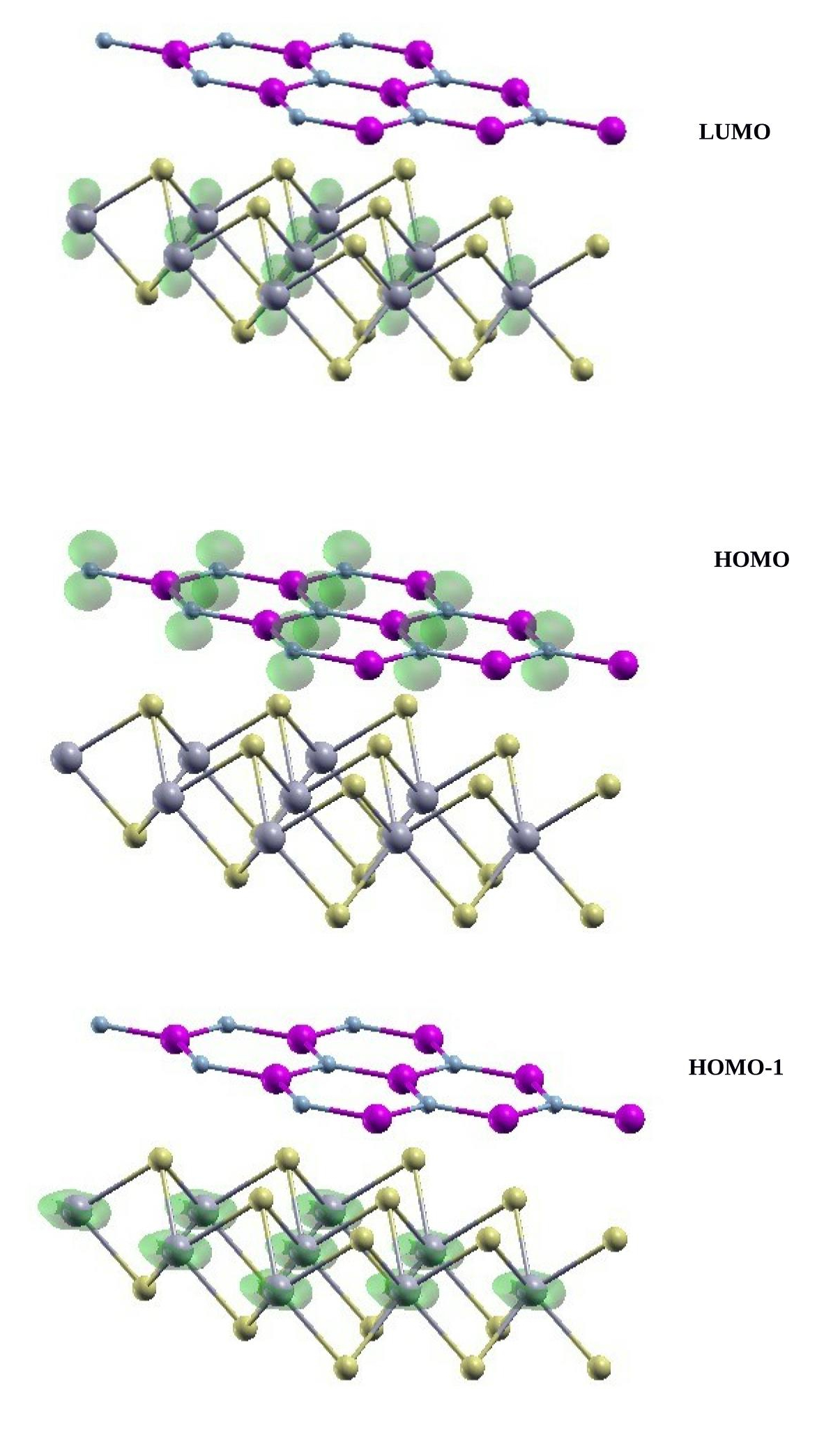
As seen more clearly in Fig. 3, the HOMO, located at K, mainly consists of the N orbitals while the LUMO, located at Q, is mainly due to W orbitals.
The interaction between the two layers increases also the spin-orbit splitting of the conduction bands at K to 0.042 eV with respect to the isolated WS2. This is not unexpected because it has already been shown that charge transfer and strain can modify the spin-orbit splitting of two dimensional materials.Absor et al. 2016; Guo et al. 2019
For what concerns DFT level of approximation, we can then affirm that the AlN/WS2 is a type II heterostructure, hence suggesting it could have promising properties for charge separation in photo-voltaic/photo-catalytic devices.Liao et al. 2014
In order to confirm this interesting result,
we need to go beyond DFT to better take into account exchange and correlation effects. We hence applied the perturbative one-shot GW method to AlN/WS2 and to the separated layers. It is worth to remember that in this work, differently from ref. Liao et al. 2014, SOC are included both in DFT and in MBPT calculations Marsili et al. 2021a.
III.2 Quasi-particle effects
We report in Table 2 the direct and indirect gap at the different levels of approximation of all the three systems AlN, WS2, and AlN/WS2. We discuss here the results for the relaxed AlN/WS2 structure (3rd row in table 2). While the constrained structure (last row in table 2) will be discussed in section III.3.1.
The GW correction in AlN opens the gap up to 5.61 eV without changing its position in space.
In WS2, instead, the calculated GW corrections open the gap and make WS2 an indirect gap material with the minimum gap located between K= and Q= Shi et al. 2013b.
The GW also reduces the spin-orbit splitting of the lowest conduction bands at K to 0.016 eV.
Now we move the AlN/WS2 heterostructure. The accurate GW electronic band structure of the relaxed bilayer is displayed in Fig. 2. The inclusion of the GW corrections reduces the SOC splitting at K to 0.028 eV. Interestingly, the quasi-particle corrections induce an interchange of the bands close to the point. The DFT highest occupied double degenerate valence bands (HOMO), located on the nitride layer, are more down-shifted by the GW corrections than the double-degenerate valence bands (HOMO-1), located on , which then become the new VBM. In other words, the valence band which is the highest in DFT (HOMO) becomes the HOMO-1 in GW, and the band which in DFT is HOMO-1, becomes the new HOMO in GW. This band exchange is due to two reasons: first the different nature of the top valence bands belonging to the AlN and WS2, the former are mainly formed from orbitals of the N atom while the latter originate from the orbitals of the W atom, and so they acquire a different GW correction as it happens, often, in molecular systemsFaber et al. 2012. Second it is the different screening felt by the electrons in AlN or in WS2, in fact, the screening is less effective in AlN (it has a larger gap), and this causes a larger quasi-particle correction on the AlN states with respect to WS2 states.
Therefore, while at the DFT level a type II heterostructure is obtained,
the GW corrections modify this picture and give a type I system, where both top valence and bottom conduction bands belong to the WS2 subsystem.
In this context it is worth to point out that the type I band offset can be obtained only considering both SOC and many-body effectsMarsili et al. 2021b.
Indeed in a recent work by Yeganeh et al. Yeganeh et al. 2022 a type II band alignment at G0W0 level but without inclusion of SOC was found.
III.3 Optical Properties of AlN/WS2
The optical response of the HT is investigated at two different levels of theory: within the independent-QP approach at the G0W0 level, and with the inclusion of local-fields and excitonic effects by solving the BSE. In Fig. 4 we present the in-plane optical absorbance for the two cases.
In order to understand the optical properties of the heterostrucure, we start with the study of the two separated layers.
The optical properties of free standing AlN, in the energy range we are interested in, are dictated by a single excitonic peak at 4.75 eV two times degenerate, see the bottom panel of Fig. 4, dashed blue line. This direct exciton is strongly bound, has large oscillator strength and a very small radius (see Tab. 3). Because of the large GW direct gap (6.27 eV), no optical response is visible at the independent-QP level in the range here considered (0-5.5 eV, see Fig. 4 upper panel).
The optical response of WS2 (green dashed line in Fig.4) is
more complex. The schematic representation of the WS2 excitonic levels is shown in Fig. 5. The lowest exciton at 2.075 eV,
is the spin-forbidden dark and double degenerate,
generally called AD.
The first bright, also double degenerate, exciton is at 2.125 eV.
Then, the B exciton, due to spin-orbit split bands, is at 2.46 eV.
Between the A and B, a series of small peaks, called A’, coming from transitions near and with a very small dipole matrix elements, are present.
These results are in agreement with theoretical predictions and experimental dataMak et al. 2010b,Ugeda et al. 2014,Zhu et al. 2015, Palummo et al. 2015.
At higher energy other excitons (normally called C and D) due to transitions in the band-nesting region, are visible.
According to the literatureMolina-Sánchez et al. 2016, they are more difficult to converge and are also more affected by the electron-phonon interaction which is not included in the present work.
The WS2 exciton levels (see Fig. 5) are in good agreement with previous calculation of Marsili et al.Marsili et al. 2021b and the small differences are due to the different pseudo-potentials used in the calculations.
We now move to the analysis of optical properties of the AlN/WS2 bilayer.
As for WS2, the inclusion of the attractive e-h interaction on top of the GW calculations moves back the absorption spectrum toward lower energy and produce new peaks due to strongly bound excitons (orange solid lines in Fig. 4).
Hence, the AlN/WS2 HT shows substantial adsorption from visible to deep UV light. Its spectrum is very similar to the WS2 free standing one, but slightly blue shifted.
In order to understand the origin of the peaks and of the blue shift, we analyze the bands involved in the transitions.
Since, as mentioned, there is an interchange of the ordering of the GW bands, in the following, when we talk about the electronic bands involved in the excitonic transitions, we refer to the original DFT order. This is to avoid confusion in the analysis of the excitons. The first direct exciton at 2.15 eV, is dark and double degenerate, and it is mainly due to the transition between the HOMO-1 and the LUMO at the K point, with a binding energy of 0.64 eV. The first visible exciton, also twice degenerate, appears at 2.21 eV and is characterized by a binding energy Eb = 0.59 eV. It involves the same bands of the two lowest dark excitons. The exciton binding energy is smaller than that of the isolated WS2 (0.64 eV) due to the presence of the AlN layer that increases the screening of the electron-hole interaction. This reduction of the binding energy contributes to the blue shift of the excitons. The peak around 2.65 eV belongs to transition at K between the third band below the highest valence band (HOMO-2) and the second conduction band (LUMO+1), and it also has double degeneration. An analysis of the first ten excitons (most of them degenerate) of the AlN/WS2 in terms of valence-conduction transitions shows that all correspond to excitation involving just WS2 states. In fact the lowest inter-layer states between AlN and WS2 appear at an energy corresponding to the states around 2.40 eV. These states are not visible in the spectra due to their very small dipole moment. By comparing the AlN/WS2 spectra with those of the isolated AlN and WS2 (see Fig.4) we can conclude that the dominant contribution comes from WS2. AlN contribution is limited to the high energy region due to the large optical gap of about 4.6 eVPrete et al. 2020 but, indirectly, affects the WS2 through the increase of the screening and, as we will discuss in the next section, through the lattice mismatch.
III.3.1 Effect of the substrate
As shown in Fig. 4, lower panel, the first exciton in AlN/WS2 is blue-shifted by about 0.1 eV with respect to the first exciton of isolated WS2. This is a puzzling result since several experiments and theoretical calculations show an opposite trend,Latini et al. 2015; Ugeda et al. 2014: an increasing of screening tends to red-shift the optical spectra. But care must be taken when directly comparing two spectra. Indeed, several (interconnected) effects are responsible of the final change in the spectra (Fig. 4): the variation of the screening, the variation of the direct gap and the change in the lattice constant. In order to test and disentangle these two effects, we also simulate an AlN/WS2 bilayer forcing the lattice constant to be the same of the isolated WS2 monolayer (a= Å). In this case we find that the direct gap reduces of eV with respect to the isolated WS2, due to the additional screening generated by the presence of the AlN layer. On the other hand, as we have discussed before, see Tab. 1, the full relaxation of the bilayer induces a small compressive strain on WS2 (a= Å) in the HT. This increases the direct gap of with respect to the unrelaxed bilayer (constrained to have a=3.16 Å) and leaves the binding energy unchanged. This means that the variation of the lattice constant induces a change in the gap larger than the one due to
AlN layer screening.
The small strain applied has then essentially no effect on the excitonic binding energy, consistently with other worksLechifflart et al. 2022.
To summarize,
this explains why the fully relaxed heterostructure has a larger GW gap than the isolated WS2, even in the presence of a larger screening.
This finding, combined with the reduction of the excitonic binding energy due to the substrate (AlN), explains the blue-shift of the first exciton in the Fig. 4.
III.3.2 Exciton model
Finally, it is worth to notice that a simple 2D excitonic model based on the Rytova-Keldysh approach Rytova 2018; Keldysh 1979; Pulci et al. 2015; Cudazzo et al. 2011 would give reasonable results, predicting the trend of the excitonic binding energies close to the ab-initio values.
Within this model, the Hamiltonian which describe the interaction of an electron-hole pair in a homogeneous 2D sheet with parabolic bands is given by
| (2) |
with exciton reduced mass and the statically screened electron-hole attraction potential:
| (3) |
Here, is the Struve function, the Neumann Bessel function of the second kind, and is the screening radius: with the static electronic sheet polarizability.
Although the error is quite large (see Tab. 3) this method confirms to be a cheap, fast way to obtain qualitative results. The simplicity of this method relies on the fact that the effective masses and polarizabilities are the only needed ingredients, and both can be easily obtained within DFT.
| m/m (me) | Re (a.u.) | Eb (eV) | rexc (Å) | |
|---|---|---|---|---|
| AlN | 1.5/0.66 | 2.2 | 1.79(2.3) | 3.4 |
| WS2 | 0.42/0.44 | 13.0 | 0.64(0.5) | 11.4 |
| AlNWS2 | 0.41/0.38 | 15.6 | 0.59(0.4) | 12.8 |
IV Conclusions
In summary, we have presented a study on a novel AlN/WS2 vdW heterostructure. Its negative formation energy as well as its small lattice mismatch between the constituent monolayers suggests that it should be possible to synthesize it. The analysis of the band alignment and decomposed partial charge density of the heterostructure shows that a calculation at the DFT level is not sufficient to identify the character of the heterostructure. The GW inverts the band order transforming the heterostructure from type II to type I. The subsequent Bethe-Salpeter calculation of optical excitations confirms this result. All the lowest optical excition, dark or bright, belong to the WS2 monolayer part. These results suggest that a simple identification of heterostructures by means of local or semi-local functional in DFT may fail when compared with more advanced methods as GW plus Bethe-Salpeter or hybrid functionals.
Finally, the optical spectrum of the heterostructure is very similar to the one of the isolated WS2, with small differences arising from the presence of the substrate, which acts through the strain and through the screening. We demonstrate that the AlN substrate modifies only slightly the electronic and optical properties of WS2 and therefore could be employed as an excellent alternative insulating substrate, acting as gate dielectric material, to the most common used h-BN.Prete et al. 2020
V acknowledgments
The research leading to these results has received funding from the European Union Seventh Framework Program under grant agreement no. 7 85219 Graphene Core2. C.A. acknowledges A. Saul and K. Boukari for the management of the computer cluster Rosa. CPU time was also granted by CINECA (ISCRA-B and ISCRA-C) and CRESCO ENEA HPC centers. This publication is based upon work from COST Action TUMIEE CA17126, supported by COST (European Cooperation in Science and Technology). O.P. and M.P. acknowledge financial funding from the EU MSCA-RISE project DiSeTCom (HORIZON2020, GA 823728). M.P. acknowledges Tor Vergata University Project 2021 TESLA. O.P. acknowledges fundings from PRIN 2020 ”PHOTO”.
VI Abbreviations
The following abbreviations are used in this manuscript:
| ALD | Atomic layer deposition |
| BSE | Bethe-Salpeter Equation |
| CBM | Conduction band minimum |
| DFT | Density Functional Theory |
| GGA | Generalized gradient approximation |
| HOMO | highest occupied molecular orbital |
| HT | Heterostructure |
| LED | Light emitting device |
| ML | Monolayer |
| MBPT | Many-body perturbation theory |
| LUMO | Lowest unoccupied molecular orbital |
| PDOS | Projected density of states |
| PV | Photo-voltaic |
| SOC | Spin orbit coupling |
| TMD | transition metal dichalcogenides |
| VBM | Valence band maximum |
References
- Geim and Novoselov (2010) A. K. Geim and K. S. Novoselov, in Nanosc. and Tech.: A Collection of Reviews from Nat. Journ. (World Scientific, 2010) pp. 11–19.
- Ponraj et al. (2016) J. S. Ponraj, Z.-Q. Xu, S. C. Dhanabalan, H. Mu, Y. Wang, J. Yuan, P. Li, S. Thakur, M. Ashrafi, K. Mccoubrey, et al., Nanotechnology 27, 462001 (2016).
- Lin et al. (2016) Z. Lin, A. McCreary, N. Briggs, S. Subramanian, K. Zhang, Y. Sun, X. Li, N. J. Borys, H. Yuan, S. K. Fullerton-Shirey, et al., 2D Materials 3, 042001 (2016).
- Li et al. (2016) M.-Y. Li, C.-H. Chen, Y. Shi, and L.-J. Li, Materials Today 19, 322 (2016).
- Brozzesi et al. (2022) S. Brozzesi, C. Attaccalite, F. Buonocore, G. Giorgi, M. Palummo, and O. Pulci, Nanomaterials 12 (2022), 10.3390/nano12122118.
- Gao et al. (2012) G. Gao, W. Gao, E. Cannuccia, J. Taha-Tijerina, L. Balicas, A. Mathkar, T. Narayanan, Z. Liu, B. K. Gupta, J. Peng, et al., Nano letters 12, 3518 (2012).
- Splendiani et al. (2010) A. Splendiani, L. Sun, Y. Zhang, T. Li, J. Kim, C.-Y. Chim, G. Galli, and F. Wang, Nano Letters 10, 1271 (2010), pMID: 20229981, https://doi.org/10.1021/nl903868w .
- Mak et al. (2010a) K. F. Mak, C. Lee, J. Hone, J. Shan, and T. F. Heinz, Phys. Rev. Lett. 105, 136805 (2010a).
- Rasmussen and Thygesen (2015) F. A. Rasmussen and K. S. Thygesen, The Journal of Physical Chemistry C 119, 13169 (2015).
- Chen et al. (2018) H.-Y. Chen, M. Palummo, D. Sangalli, and M. Bernardi, Nano letters 18, 3839 (2018).
- Bernardi et al. (2017) M. Bernardi, C. Ataca, M. Palummo, and J. C. Grossman, Nanophotonics 6, 479 (2017).
- Gusakova et al. (2017) J. Gusakova, X. Wang, L. L. Shiau, A. Krivosheeva, V. Shaposhnikov, V. Borisenko, V. Gusakov, and B. K. Tay, physica status solidi (a) 214, 1700218 (2017), https://onlinelibrary.wiley.com/doi/pdf/10.1002/pssa.201700218 .
- Kecik et al. (2018) D. Kecik, A. Onen, M. Konuk, E. Gürbüz, F. Ersan, S. Cahangirov, E. Aktürk, E. Durgun, and S. Ciraci, Applied Physics Reviews 5, 011105 (2018).
- Wang et al. (2021a) Z. Wang, G. Wang, X. Liu, S. Wang, T. Wang, S. Zhang, J. Yu, G. Zhao, and L. Zhang, J. Mater. Chem. C 9, 17201 (2021a).
- Sahin et al. (2009) H. Sahin, S. Cahangirov, M. Topsakal, E. Bekaroglu, E. Akturk, R. T. Senger, and S. Ciraci, Phys. Rev. B 80, 155453 (2009).
- Prete et al. (2017) M. S. Prete, A. Mosca Conte, P. Gori, F. Bechstedt, and O. Pulci, Applied Physics Letters 110, 012103 (2017).
- Prete et al. (2018) M. S. Prete, O. Pulci, and F. Bechstedt, Phys. Rev. B 98, 235431 (2018).
- Prete et al. (2020) M. S. Prete, D. Grassano, O. Pulci, I. Kupchak, V. Olevano, and F. Bechstedt, Scientific reports 10, 1 (2020).
- Mohanta et al. (2019) M. K. Mohanta, A. Rawat, N. Jena, Dimple, R. Ahammed, and A. De Sarkar, ACS applied materials & interfaces 12, 3114 (2019).
- Wang et al. (2021b) S. Wang, Y. Hu, Y. Wei, W. Li, N. T. Kaner, Y. Jiang, J. Yang, and X. Li, Physica E: Low-dimensional Systems and Nanostructures 130, 114674 (2021b).
- Rawat et al. (2021) A. Rawat, A. Arora, and A. De Sarkar, Applied Surface Science 563, 150304 (2021).
- Jiang et al. (2021) Y. Jiang, S. Chen, W. Zheng, B. Zheng, and A. Pan, Light: Science & Applications 10, 72 (2021).
- Varsano et al. (2020) D. Varsano, M. Palummo, E. Molinari, and M. Rontani, Nature Nanotechnology 15, 367 (2020).
- Sun et al. (2022) B. Sun, W. Zhao, T. Palomaki, Z. Fei, E. Runburg, P. Malinowski, X. Huang, J. Cenker, Y.-T. Cui, J.-H. Chu, X. Xu, S. S. Ataei, D. Varsano, M. Palummo, E. Molinari, M. Rontani, and D. H. Cobden, Nature Physics 18, 94 (2022).
- Chang et al. (2022) S.-J. Chang, S.-Y. Wang, Y.-C. Huang, J. H. Chih, Y.-T. Lai, Y.-W. Tsai, J.-M. Lin, C.-H. Chien, Y.-T. Tang, and C. Hu, Applied Physics Letters 120, 162102 (2022), https://doi.org/10.1063/5.0083809 .
- Song et al. (2021) Y. Song, Y. He, Y. Li, H. Wei, P. Qiu, Q. Huang, Z. He, J. Die, M. Peng, and X. Zheng, Crystal Growth and Design 21, 1778 (2021).
- Desai et al. (2020) P. Desai, A. K. Ranade, M. Shinde, B. Todankar, R. D. Mahyavanshi, M. Tanemura, and G. Kalita, Journal of Materials Science: Materials in Electronics 31, 2040 (2020).
- Yan et al. (2018) P. Yan, Q. Tian, G. Yang, Y. Weng, Y. Zhang, J. Wang, F. Xie, and N. Lu, RSC Adv. 8, 33193 (2018).
- Liao et al. (2014) J. Liao, B. Sa, J. Zhou, R. Ahuja, and Z. Sun, The Journal of Physical Chemistry C 118, 17594 (2014).
- Perdew et al. (2008) J. P. Perdew, A. Ruzsinszky, G. I. Csonka, O. A. Vydrov, G. E. Scuseria, L. A. Constantin, X. Zhou, and K. Burke, Physical review letters 100, 136406 (2008).
- van Setten et al. (2018) M. J. van Setten, M. Giantomassi, E. Bousquet, M. J. Verstraete, D. R. Hamann, X. Gonze, and G.-M. Rignanese, Computer Physics Communications 226, 39 (2018).
- Giannozzi et al. (2009) P. Giannozzi et al., J. Phys. Condens. Matter 21, 395502 (2009), http://www.quantum-espresso.org.
- Hamada (2014) I. Hamada, Physical Review B 89, 121103 (2014).
- Rozzi et al. (2006) C. A. Rozzi, D. Varsano, A. Marini, E. K. Gross, and A. Rubio, Physical Review B 73, 205119 (2006).
- Sangalli et al. (2019) D. Sangalli, A. Ferretti, H. Miranda, C. Attaccalite, I. Marri, E. Cannuccia, P. Melo, M. Marsili, F. Paleari, A. Marrazzo, et al., Journal of Physics: Condensed Matter 31, 325902 (2019).
- Aryasetiawan and Gunnarsson (1998) F. Aryasetiawan and O. Gunnarsson, Reports on Progress in Physics 61, 237 (1998).
- Strinati (1988) G. Strinati, La Rivista del Nuovo Cimento (1978-1999) 11, 1 (1988).
- Marsili et al. (2021a) M. Marsili, A. Molina-Sánchez, M. Palummo, D. Sangalli, and A. Marini, Phys. Rev. B 103, 155152 (2021a).
- Bruneval and Gonze (2008) F. Bruneval and X. Gonze, Physical Review B 78, 085125 (2008).
- Godby and Needs (1989) R. Godby and R. Needs, Physical review letters 62, 1169 (1989).
- Stankovski et al. (2011) M. Stankovski, G. Antonius, D. Waroquiers, A. Miglio, H. Dixit, K. Sankaran, M. Giantomassi, X. Gonze, M. Côté, and G.-M. Rignanese, Physical Review B 84, 241201 (2011).
- Deng et al. (2018) S. Deng, L. Li, and M. Li, Physica E: Low-dimensional Systems and Nanostructures 101, 44 (2018).
- Shi et al. (2013a) H. Shi, H. Pan, Y.-W. Zhang, and B. I. Yakobson, Phys. Rev. B 87, 155304 (2013a).
- Drüppel et al. (2018) M. Drüppel, T. Deilmann, J. Noky, P. Marauhn, P. Krüger, and M. Rohlfing, Phys. Rev. B 98, 155433 (2018).
- Lee et al. (2010) K. Lee, É. D. Murray, L. Kong, B. I. Lundqvist, and D. C. Langreth, Physical Review B 82, 081101 (2010).
- Bernardi et al. (2013) M. Bernardi, M. Palummo, and J. C. Grossman, Nano Letters 13, 3664 (2013).
- Rawat et al. (2019) A. Rawat, R. Ahammed, Dimple, N. Jena, M. K. Mohanta, and A. De Sarkar, The Journal of Physical Chemistry C 123, 12666 (2019).
- Re Fiorentin et al. (2020) M. Re Fiorentin, G. Cicero, and M. Palummo, Phys. Rev. Materials 4, 074009 (2020).
- Bastonero et al. (2021) L. Bastonero, G. Cicero, M. Palummo, and M. Re Fiorentin, ACS Applied Materials & Interfaces 13, 43615 (2021).
- Absor et al. (2016) M. A. U. Absor, H. Kotaka, F. Ishii, and M. Saito, Phys. Rev. B 94, 115131 (2016).
- Guo et al. (2019) S. Guo, H. Zheng, Y. Wang, and J. Zhang, AIP Advances 9, 075304 (2019).
- Shi et al. (2013b) H. Shi, H. Pan, Y.-W. Zhang, and B. I. Yakobson, Phys. Rev. B 87, 155304 (2013b).
- Faber et al. (2012) C. Faber, I. Duchemin, T. Deutsch, C. Attaccalite, V. Olevano, and X. Blase, Journal of Materials Science 47, 7472 (2012).
- Marsili et al. (2021b) M. Marsili, A. Molina-Sánchez, M. Palummo, D. Sangalli, and A. Marini, Physical Review B 103, 155152 (2021b).
- Yeganeh et al. (2022) M. Yeganeh, A. Boochani, A. Yari, M. Amiri, and A. T. Shahraki, Materials Science in Semiconductor Processing 148, 106772 (2022).
- Mak et al. (2010b) K. F. Mak, C. Lee, J. Hone, J. Shan, and T. F. Heinz, Physical review letters 105, 136805 (2010b).
- Ugeda et al. (2014) M. M. Ugeda, A. J. Bradley, S.-F. Shi, F. H. da Jornada, Y. Zhang, D. Y. Qiu, W. Ruan, S.-K. Mo, Z. Hussain, Z.-X. Shen, F. Wang, S. G. Louie, and M. F. Crommie, Nature Materials 13, 1091 (2014).
- Zhu et al. (2015) B. Zhu, X. Chen, and X. Cui, Scientific Reports 5, 9218 (2015).
- Palummo et al. (2015) M. Palummo, M. Bernardi, and J. C. Grossman, Nano Letters 15, 2794 (2015).
- Molina-Sánchez et al. (2016) A. Molina-Sánchez, M. Palummo, A. Marini, and L. Wirtz, Phys. Rev. B 93, 155435 (2016).
- Latini et al. (2015) S. Latini, T. Olsen, and K. S. Thygesen, Physical Review B 92, 245123 (2015).
- Lechifflart et al. (2022) P. Lechifflart, F. Paleari, and C. Attaccalite, SciPost Physics 12, 145 (2022).
- Rytova (2018) N. S. Rytova, arXiv preprint arXiv:1806.00976 (2018).
- Keldysh (1979) L. Keldysh, JETP Letters 29, 658 (1979).
- Pulci et al. (2015) O. Pulci, M. Marsili, V. Garbuio, P. Gori, I. Kupchak, and F. Bechstedt, Physica Status Solidi (b) 252, 72 (2015).
- Cudazzo et al. (2011) P. Cudazzo, I. V. Tokatly, and A. Rubio, Physical Review B 84, 085406 (2011).