Resonant tunneling in graphene-ferroelectric-graphene junctions
Abstract
We study tunnel junctions consisting of a two-dimensional ferroelectric material sandwiched between graphene electrodes. We formulate a theory for the interplay of the polarization and induced free charges in such devices, taking into account quantum capacitance effects. We predict a gate sensitive voltage difference across the polar domains, which can be measured using electrostatic force microscopy. Incorporating this electrostatic theory in the tunneling current-voltage characteristics, we identify a resonance peak associated with aligned Dirac cones as a highly sensitive probe of the polarization. This opens the way for device applications with few atom-thick polar layers acting as readable ultra-high-density memory.
I Introduction
Recent breakthroughs in two-dimensional (2D) van der Waals materials led to the experimental realization of a new form of ferroelectricity (FE) Li and Wu 2017; Yasuda et al. 2021; Stern Vizner et al. 2021; Weston et al. 2022; de la Barrera et al. 2021; Deb et al. 2022. This newly discovered interfacial ferroelectricity results from polar stacking configurations that break inversion symmetry, such as in AB or BA stacked hexagonal boron nitride (h-BN) bilayer Yasuda et al. 2021; Stern Vizner et al. 2021 or other 2D materials Weston et al. 2022; de la Barrera et al. 2021; Deb et al. 2022. Remarkably, the resulting polarization can be flipped Stern Vizner et al. 2021 by a relative sliding of the layers by a single atomic distance.
Understanding the response to electric fields and the nature of ferroelectricity Wu and Li 2021; Zhong et al. 2021 in these experiments requires further study and a possible distinction of these various systems Bennett 2022. In the bulk of twisted interfaces there is a Moiré-triangular lattice of alternating AB and BA regions which expand or shrink at finite field de la Barrera et al. 2021. Yet, in average over many Moiré unit cells there is no remnant polarization at zero field Bennett and Remez 2022. On the other hand, in Refs. Yasuda et al. 2021; Stern Vizner et al. 2021 hysteresis was seen, and specifically in Ref. Stern Vizner et al. 2021, the flipping of a polar domain was attributed to the sliding of a domain wall near the edge of the bilayer, rather than in the bulk Bennett 2022. Leaving the precise sliding FE mechanism aside, here we shall be concerned only with uniform AB and BA polar interfaces.
Ferroelectric tunnel junctions, consisting of a thin FE material sandwiched between two electrodes, permit reading the polarization via tunnelling electroresistance (TER) Pantel and Alexe 2010; Garcia and Bibes 2014; Tao and Wang 2016; Kang et al. 2020; Yan et al. 2022. What is the fate of interfacial polarization within a tunnel junction?
In this work, we theoretically study 2D tunnel junctions consisting of uniform AB or BA polar interfaces sandwiched by graphene electrodes, as shown in Fig. 1(a). Assuming a given value for the bare polarization , which, in principle, can be determined by ab initio methods, we focus on the interplay of the polarization and screening charges forming on the graphene electrodes. Related questions were recently addressed within density functional theory (DFT) Yang et al. 2021, where it was found that whereas metallic electrodes significantly affect the polarization of a bilayer h-BN, adding graphene spacers between the FE and metals restores the polarization and results in a significant TER. Here, we provide a phenomenological electrostatic model. We find that when one of the electrode’s Fermi level is tuned to the Dirac point, the electronic equilibration is dominated by quantum capacitance, and then a polar domain associated local voltage can be measured across the device.
We focus on basic mechanisms allowing to read out the polarization direction and magnitude from the current-voltage characteristics. One TER mechanism results from the dependence of the electrostatic tunneling barrier on the polarization orientation. We discuss a model allowing to estimate this barrier modulation in the 2D limit.
Moreover, a graphene-FE-graphene junction allows for a more sensitive finite voltage TER mechanism due to 2D momentum conservation. Resonance tunneling peaks in the characteristics were identified both in planar 2D junctions of semiconductor heterostructures Eisenstein et al. 1991; Eisenstein et al. 1992, and more recently in 2D materials Britnell et al. 2013; Mishchenko et al. 2014; Chen 2021, specifically for graphene-h-BN-graphene Britnell et al. 2013. There, the h-BN material simply acts as a barrier Yan et al. 2021; Yan et al. 2022; Yan et al. 2020, whereas the resonance peaks emerge due to momentum conserving tunneling between the graphene electrodes. The device we consider is almost the same as in Ref. Britnell et al. 2013, where now the barrier consists of a parallel stacked h-BN bilayer supporting the polar AB or BA interfaces. Such a device is expected to be a perfect candidate to employ resonance tunneling peaks as a sensitive probe of interfacial polarization, which essentially acts as an internal voltage that shifts the resonance. We indeed find using our self-consistent model a sizable shift of the resonance peak Britnell et al. 2013; Mishchenko et al. 2014; Chen 2021 for the two polarization directions.

The paper is organized as follows. After introducing the model in Sec. II, we study the Kelvin probe voltage in Sec. III. In Sec. IV we estimate the ratio of the tunneling coefficients in our device. In Sec. V we consider momentum conserving tunneling and focus on resonance peaks as a means to detect the polarization. We summarize in Sec. VI.
II Model
As shown in Fig. 1(a), we consider a tunneling junction consisting of a 2D polar interface encapsulated between two graphene sheets. Our theory is not restricted to a specific material, but for definiteness we consider parallel stacked bi-layer h-BN, having two polar stacking configurations denoted AB and BA exhibiting a finite out of plane polarization which is accounted for by an internal voltage denoted , see Fig. 1(b). A tunneling current is enabled by a bias voltage . The bottom graphene sheet is gated by a voltage . The energy describing the system is given by
| (1) | |||||
Here is the capacitance between the two graphene sheets, and is the capacitance between the bottom graphene sheet and a gate. We measure energy, charge and capacitance per unit area.
The third line encapsulates a quadratic expansion of the free energy Stern Vizner et al. 2021 around the minima for either one of the two stacking configurations denoted by . By construction, the bare KP voltage (i.e. without the electrodes) is given by for AB or BA stacking, see Fig. 1(b). Its value was measured directly using Kelvin probe force microscopy Stern Vizner et al. 2021. In addition, this term renormalizes the capacitance by the dielectric constant of the material.
The last line represents the quantum capacitance of the graphene sheets, with
| (2) |
and . is the total kinetic energy density measured from the Dirac point, valid in the vicinity of the Dirac point, and refers to holes (electrons).
The goal of this electrostatic model is to allow variations of the polarization of the AB or BA interface due to electric fields produced by the graphene electrodes.
The equilibrium configuration is obtained by minimizing the energy with respect to the charge induced on the top sheet and on the gate , and the polarization of the interface . The equation gives
| (3) |
showing that the internal polarization is affected by the electrodes. Defining the Fermi energy
| (4) |
the equations yield
| (5) | |||||
| (6) |
Eqs. (5) and (6) are subsequently solved numerically for and as function of and for either sign of the polarization .
III Kelvin probe voltage

In this section we calculate the KP voltage, which can be measured via scanning atomic force microscopy (AFM) as function of gate and bias voltages, in a setup as in Fig. 2(a). Such measurements were performed for the bare ferroelectric material Yasuda et al. 2021; Stern Vizner et al. 2021; Weston et al. 2022. Our theory addresses the renormalization of the internal polarization and the resulting total KP voltage across the electrodes.
The total voltage drop measured in a Kelvin probe setup as in Fig. 2(a) is given by
| (7) |
where we used Eq. (3). We subsequently focus on the difference of for the two polarization orientations, which can be measured by scanning the AFM tip across a stacking domain wall, see Fig. 2(a).
It is convenient to measure in units of the bare polar domains voltage by defining the Kelvin probe sensitivity (KPS)
| (8) |
The second equality, obtained from Eq. (7), shows that in the absence of charges on the electrodes.
The numerical solution for and hence the KPS is shown in Fig. 2(b) as function of bias and gate voltages. A cut with fixed in shown in Fig. 2(c). We can see that peaks when either one of the two graphene sheets is at charge neutrality and takes a value which is of the order of (and hence ). Along these peaks the charge transfer between the electrodes is small and primarily determined by quantum capacitance, and hence it very inefficiently screens electrostatically the internal polarization.
We now discuss the physics describing the tail and peaks of (or equivalently in Fig. 2(c)). The tails can be analysed by considering the quantum capacitance as a small perturbation. One can solve Eqs. (5) and (6) up to a given order in . In the absence of quantum capacitance () we have
| (9) |
Then , , and . The vanishing KPS is expected since the potential on the electrodes adjusts such as to completely screen the internal polarization. Considering a small quantum capacitance correction, , , and expanding Eq. (5) to linear order in these deviations, we obtain for
| (10) |
This is confirmed as a dashed line in Fig. 2(c).
The height of the two peaks in Fig. 2(c) can be obtained by considering the quantum capacitance of the corresponding neutralized graphene sheet as the dominant term. Consider for example the peak [nearly vertical peak ridge in Fig. 2(b)]. We can then decouple Eqs. (5) and (6) by replacing the Fermi energy of the bottom layer by . We thus obtain , yielding a peak at where for large we have . Solving the quadratic equation yields . Substituting in Eq. (8), we have . Expanding in small , yields
| (11) |
We can see that sets a voltage scale below which quantum capacitance effects set in. In our system
| (12) |
Thus, the reason that the peaks in KPS approach nearly unity is that the material property is small, but of the order of .
IV Polarization dependent tunneling coefficient
In this section we discuss the influence of the polarization on the tunneling coefficient . This effect can be understood from a polarization-dependent distortion of the electrostatic tunnel barrier Zhuravlev et al. 2005; Gerra et al. 2007, modifying the tunneling coefficient due to its exponential sensitivity .
Let us denote the tunneling amplitudes for the two polarization orientations by and define the relative barrier modulation
| (13) |
As a simple model providing an order of magnitude estimate for , consider the bottom and top graphene sheets to be located at the planes, and the two h-BN layers at the planes. The tunneling amplitude from bottom to top is given via 3-rd order perturbation theory by Brey 2014 , where are nearest layer hopping amplitudes, and is the energy in the h-BN layers. We denote by the energy gap of the bare h-BN layer at . Adding the linear potential due to the charged electrodes, . The tunneling amplitude becomes . If the two directions of polarization lead to exactly opposite charge transfer, , then . In general when inversion symmetry holds, namely when and . Finite barrier modulation results from ,
| (14) |
For sufficiently large , using Eq. (9) which ignores quantum capacitance effects, we have independently of . Assuming , this result leads to a few percent relative barrier modulation for a bias of few volts. The smallness of the effect derives from the small ratio between the voltage and the gap of h-BN, however this can be made larger in other materials. Higher may also be obtained in an asymmetric device when one electrode is weakly coupled while the other one is strongly coupled Rogée et al. 2022.
We note that the TER is defined [see Eq. (18] below and Refs. Tao and Wang 2016; Kang et al. 2020; Yan et al. 2022) in terms of the currents at finite bias voltage. Our definition of the relative barrier modulation in Eq. (13) allows to separate the effect of the modulation of the barrier itself, which leads to a relatively week contribution to TER, from the effects associated with momentum conserving tunneling between two graphene sheets, to be considered in the next section.
V Momentum conserving Tunneling
In this section we consider 2D momentum conserving tunneling through the polar interface. In conventional tunnel junctions 2D momentum conservation leads to a resonance peak in the characteristics corresponding to two aligned Dirac cones Britnell et al. 2013; Mishchenko et al. 2014; Chen 2021. Our goal is to incorporate the interfacial polarization into the resonant condition, yielding a sensitive probe of the polarization orientation and magnitude.
Following the model outlined in Ref. Britnell et al. 2013, we start with a Fermi golden rule expression for the tunneling current
| (15) |
In this section, in order to disentangle the TER effects of the previous chapter with effects of momentum conservation, we assume for simplicity . Here, are Fermi functions and are the electron () and hole () bands in the bottom or top sheet , respectively (see Fig. 3). This process describes tunneling of an electron from an occupied momentum state in the bottom layer to an unoccupied state with momentum at the top layer, measured from the respective Dirac point in a given valley. The scattering potential contains a phenomenological momentum dependence . Here is a momentum shift between the top and bottom Dirac points (at momentum in the Brillouin zone) due to a relative twist of the layers by angle . The limit corresponds to momentum conserving tunneling. A finite phenomenologically describes non-momentum-conserving tunneling processes e.g. due to short-range disorder or the Moiré pattern of either the h-BN or its interface with graphene. We take Britnell et al. 2013. The typical energy band diagram in the presence of a bias voltage is shown in Fig. 3(a). Since and mark the distance of these Fermi levels from the corresponding Dirac point; from Eq. (5) it follows that the energy difference of the two Dirac points is given precisely by , as marked in Fig. 3(a).

V.1 Zero twist angle
When the two graphene sheets are perfectly aligned we have . For any energy within the voltage window, the two momenta and belong to two concentric circles in momentum space, as denoted in Fig. 3(b). The energy displacement of the Dirac cones, , is controlled by the bias voltage. When these two circles in momentum space overlap, for all energies, leading to a resonant current peak.
The resonance peak can be obtained by performing the angular integration, leading to
| (16) |
This yields a single integral that we evaluate numerically.

Fig. 4 shows a color map of the current versus and for a specific polarization direction. As a guide to the eye, this figure displays the charge neutrality curves of either bottom or top graphene sheets. We also plot the curve where . A cut of the curve for either direction of the polarization for fixed is shown in the right-top inset of Fig. 4. We can see a pronounced resonance peak positioned precisely at at which where the Dirac cones overlap. This occurs for different resonant voltages for the two polarization orientations.
The line shape of the peak versus stems from the implicit dependence of on the latter, and takes the form
| (17) |
We can also observe a plateau in the curve in Fig. 4 which terminates at (at point 5). As shown in the energy diagrams in Fig. 4, this corresponds to a threshold for transport through the midway energy between the two Dirac points, see green dashed lines. At the threshold this specific energy enters into the voltage window Feenstra et al. 2012.
We note that the shifted resonance peaks lead to a significant TER Wu et al. 2020; Yan et al. 2021; Yan et al. 2022, defined as
| (18) |
as shown in Fig. 4 (right-bottom inset). The role of our definition of the relative barrier modulation in Sec. IV meant to separate this effect from the modification of the tunneling amplitudes for the two polarization directions.
V.2 Finite twist angle
Tunneling between twisted graphene sheets has been discussed in numerous theory Feenstra et al. 2012; de la Barrera et al. 2014 and experimental Mishchenko et al. 2014 works. Whereas at zero twist, there is a single resonance condition at which the two Dirac cones completely overlap, at a finite twist angle there is a momentum shift between the Dirac points, given by for . Thus equi-energy contours of the bottom and top layers are non-concentric circles, see Fig. 3(c). Upon tuning their relative energy there are two situations where the Dirac cones are tangential,
| (19) |
The calculated current with a finite twist angle of is shown in the color plot of Fig. 5. We can clearly see that the pair of resonance peaks, also shown along a cut of fixed gate, overlaps with the condition Eq. (19). The corresponding dispersion relations are shown in the top insets of Fig. 5. The sensitivity of the resonant peaks to different orientation of the polarization can be enhanced by tuning the gate such that the resonance peaks will occur near the charge neutrality condition of one graphene sheet. This is indeed seen for the cut of the curve at .

V.3 Dependence on G-G twist angle
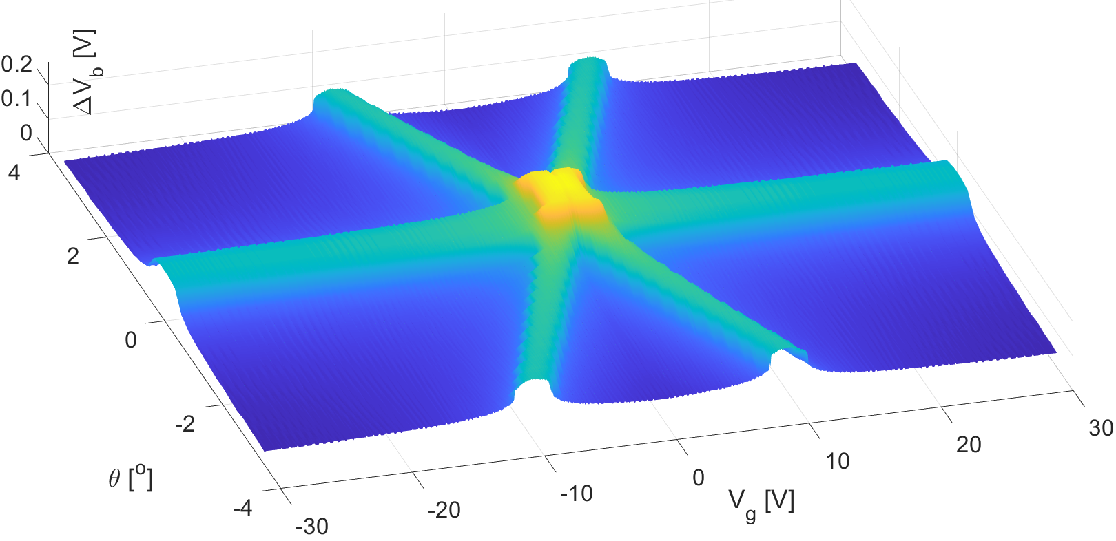
We now discuss the twist-angle dependence of the resonance peaks. At we observed a resonance peak whose position depends on the polarization orientation . The peak separation is a sensitive probe of the polarization, see Figs. 4 and 5.
The peak separation is plotted in Fig. 6 as a function of and . For zero twist angle we have seen in the inset of Fig. 4 that for . We can see in Fig. 6 that at this significant peak separation persists for any value of , and peaks near . But at finite twist angle, the peak separation becomes visible only for specific values of . For example for , as we have seen in the inset of Fig. 5, the peak separation is resolved only near . As discussed, this maximal sensitivity occurs when both Eq. (19) holds and one graphene sheet is at charge neutrality . Therefore, in order to achieve good sensitivity in terms of resonance peak separation, one should operate such a device at specific twist angle dependent value of the gate voltage.
The slope of the high sensitivity spokes in the plane can be obtained analytically. By solving Eqs. (5) and (6), with the added condition of Eq. (19), we obtain the expression for the bias voltage at which the peak occurs as a function of and . For a given twist angle, the difference of such bias voltage for the two orientations of the polarization, representing the peak separation, is extremized analytically with respect to . For large enough gate voltages (outside the range where both graphene sheets are near the charge neutrality), we find
| (20) |
which perfectly fits the spokes in Fig. 6 (not shown).
VI Summary
To summarize, in this work we studied graphene-FE-graphene junctions. We focused on the self-consistent interplay of the polarization with the electrostatics and quantum capacitance of the graphene electrodes. We first asked whether experiments will detect a polar domain voltage across the conducting graphene electrodes, and discovered that a finite signal appears only upon gate tuning of one of the Dirac electrodes to charge neutrality.
Moving to the tunneling current, we studied two mechanisms for its dependence on the polarization direction. First, we discussed a dependence of the tunneling coefficient on the polarization. This barrier sensitivity becomes sizable upon increasing the bias voltage which leads to a device asymmetry, but is relatively small at zero bias for available values of gate voltages. We then considered 2D momentum conserving tunneling, and showed that one can detect the actual value of the polarization via a shift in the voltage axis of a resonant peak occurring in the characteristics due to the alignment of the Dirac cones. This resulted in a sizable TER.
In order to switch from one state to the other, one would need, in practice, to slide a domain wall separating AB and BA stacking through the tunneling region. This could be achieved by tuning the bias above the switching point. This process goes beyond the presented model.
Our results apply to Moiré superlattice materials such as transition metal dichalcogenides. We hope that our theory will serve as a basis for analysis of near-future FE tunnneling experiments.
VII Acknowledgments
We thank discussions with Moshe Ben Shalom, Igor Rozhansky, Simon Sallah Atri and Hadar Steinberg. This project received funding from the European Research Council (ERC) under the European Union’s Horizon 2020 research and innovation program under grant agreement No 951541.
References
- Li and Wu (2017) Lei Li and Menghao Wu, “Binary compound bilayer and multilayer with vertical polarizations: two-dimensional ferroelectrics, multiferroics, and nanogenerators,” ACS nano 11, 6382–6388 (2017).
- Yasuda et al. (2021) Kenji Yasuda, Xirui Wang, Kenji Watanabe, Takashi Taniguchi, and Pablo Jarillo-Herrero, “Stacking-engineered ferroelectricity in bilayer boron nitride,” Science 372, 1458–1462 (2021).
- Stern Vizner et al. (2021) Maayan Stern Vizner, Yuval Waschitz, Wei Cao, Iftach Nevo, Kenji Watanabe, Takashi Taniguchi, Eran Sela, Michael Urbakh, Oded Hod, and Moshe Ben Shalom, “Interfacial ferroelectricity by van der waals sliding,” Science 372, 142–1466 (2021).
- Weston et al. (2022) Astrid Weston, Eli G Castanon, Vladimir Enaldiev, Fabio Ferreira, Shubhadeep Bhattacharjee, Shuigang Xu, Héctor Corte-León, Zefei Wu, Nicholas Clark, Alex Summerfield, et al., “Interfacial ferroelectricity in marginally twisted 2d semiconductors,” Nat. Nanotechnol. , 1–6 (2022).
- de la Barrera et al. (2021) Sergio C de la Barrera, Qingrui Cao, Yang Gao, Yuan Gao, Vineetha S Bheemarasetty, Jiaqiang Yan, David G Mandrus, Wenguang Zhu, Di Xiao, and Benjamin M Hunt, “Direct measurement of ferroelectric polarization in a tunable semimetal,” Nat. Commun. 12, 1–9 (2021).
- Deb et al. (2022) Swarup Deb, Wei Cao, Noam Raab, Kenji Watanabe, Takashi Taniguchi, Moshe Goldstein, Leeor Kronik, Michael Urbakh, Oded Hod, and Moshe Ben Shalom, “Cumulative polarization coexisting with conductivity at interfacial ferroelectrics,” (2022), 10.48550/ARXIV.2206.12215.
- Wu and Li (2021) Menghao Wu and Ju Li, “Sliding ferroelectricity in 2d van der waals materials: Related physics and future opportunities,” Proc. Natl. Acad. Sci. U.S.A. 118, e2115703118 (2021).
- Zhong et al. (2021) Tingting Zhong, Yangyang Ren, Zhuhua Zhang, Jinhua Gao, and Menghao Wu, “Sliding ferroelectricity in two-dimensional moa 2 n 4 (a= si or ge) bilayers: high polarizations and moiré potentials,” J. Mater. Chem A 9, 19659–19663 (2021).
- Bennett (2022) Daniel Bennett, “Theory of polar domains in moiré heterostructures,” Phys. Rev. B 105, 235445 (2022).
- Bennett and Remez (2022) Daniel Bennett and Benjamin Remez, “On electrically tunable stacking domains and ferroelectricity in moiré superlattices,” NPJ 2D Mater. Appl. 6 (2022), 10.1038/s41699-021-00281-6.
- Pantel and Alexe (2010) Daniel Pantel and Marin Alexe, “Electroresistance effects in ferroelectric tunnel barriers,” Phys. Rev. B 82, 134105 (2010).
- Garcia and Bibes (2014) Vincent Garcia and Manuel Bibes, “Ferroelectric tunnel junctions for information storage and processing,” Nat. Commun. 5, 1–12 (2014).
- Tao and Wang (2016) LL Tao and J Wang, “Ferroelectricity and tunneling electroresistance effect driven by asymmetric polar interfaces in all-oxide ferroelectric tunnel junctions,” Appl. Phys. Lett. 108, 062903 (2016).
- Kang et al. (2020) Lili Kang, Peng Jiang, Hua Hao, Yanhong Zhou, Xiaohong Zheng, Lei Zhang, and Zhi Zeng, “Giant tunneling electroresistance in two-dimensional ferroelectric tunnel junctions with out-of-plane ferroelectric polarization,” Phys. Rev. B. 101, 014105 (2020).
- Yan et al. (2022) Zhi Yan, Zeyu Li, Yulei Han, Zhenhua Qiao, and Xiaohong Xu, “Giant tunneling magnetoresistance and electroresistance in - in 2 se 3-based van der waals multiferroic tunnel junctions,” Phys. Rev. B. 105, 075423 (2022).
- Yang et al. (2021) Jie Yang, Jun Zhou, Jing Lu, Zhaochu Luo, Jinbo Yang, and Lei Shen, “Sliding ferroelectric tunnel junctions,” arXiv:2112.02886 (2021).
- Eisenstein et al. (1991) James P. Eisenstein, Thomas. J. Gramila, Loren N. Pfeiffer, and K. W. West, “Probing a two-dimensional fermi surface by tunneling,” Phys. Rev. B 44, 6511–6514 (1991).
- Eisenstein et al. (1992) James P. Eisenstein, Loren N Pfeiffer, and KW West, “Coulomb barrier to tunneling between parallel two-dimensional electron systems,” Phys. Rev. Lett. 69, 3804 (1992).
- Britnell et al. (2013) L. Britnell, R. V. Gorbachev, A. K. Geim, L. A. Ponomarenko, A. Mishchenko, M. T. Greenaway, T. M. Fromhold, K. S. Novoselov, and L. Eaves, “Resonant tunnelling and negative differential conductance in graphene transistors,” Nat. Commun. 4 (2013), 10.1038/ncomms2817.
- Mishchenko et al. (2014) Artem Mishchenko, JS Tu, Y Cao, Roman V Gorbachev, JR Wallbank, MT Greenaway, VE Morozov, SV Morozov, MJ Zhu, SL Wong, et al., “Twist-controlled resonant tunnelling in graphene/boron nitride/graphene heterostructures,” Nat. Nanotechnol. 9, 808–813 (2014).
- Chen (2021) Julian Chen, Introduction to Scanning Tunneling Microscopy, 3rd ed. (Oxford University Press, 2021).
- Yan et al. (2021) Zhi Yan, Xin Jia, Xiaowen Shi, Xinlong Dong, and Xiaohong Xu, “Barrier-dependent electronic transport properties in two-dimensional mnbi2te4-based van der waals magnetic tunnel junctions,” Appl. Phys. Lett. 118, 223503 (2021).
- Yan et al. (2020) Zhi Yan, Ruiqiang Zhang, Xinlong Dong, Shifei Qi, and Xiaohong Xu, “Significant tunneling magnetoresistance and excellent spin filtering effect in cri 3-based van der waals magnetic tunnel junctions,” Phys. Chem. Chem. Phys. 22, 14773–14780 (2020).
- Zhuravlev et al. (2005) M Ye Zhuravlev, Renat F Sabirianov, SS Jaswal, and Evgeny Y Tsymbal, “Giant electroresistance in ferroelectric tunnel junctions,” Phys. Rev. Lett. 94, 246802 (2005).
- Gerra et al. (2007) G Gerra, AK Tagantsev, and N Setter, “Ferroelectricity in asymmetric metal-ferroelectric-metal heterostructures: a combined first-principles–phenomenological approach,” Phys. Rev. Lett. 98, 207601 (2007).
- Brey (2014) Luis Brey, “Coherent tunneling and negative differential conductivity in a graphene/-bn/graphene heterostructure,” Phys. Rev. Appl. 2, 014003 (2014).
- Rogée et al. (2022) Lukas Rogée, Lvjin Wang, Yi Zhang, Songhua Cai, Peng Wang, Manish Chhowalla, Wei Ji, and Shu Ping Lau, “Ferroelectricity in untwisted heterobilayers of transition metal dichalcogenides,” Science 376, 973–978 (2022).
- Feenstra et al. (2012) Randall M Feenstra, Debdeep Jena, and Gong Gu, “Single-particle tunneling in doped graphene-insulator-graphene junctions,” J. Appl. Phys. 111, 043711 (2012).
- Wu et al. (2020) Jiangbin Wu, Hung-Yu Chen, Ning Yang, Jun Cao, Xiaodong Yan, Fanxin Liu, Qibin Sun, Xi Ling, Jing Guo, and Han Wang, “High tunnelling electroresistance in a ferroelectric van der waals heterojunction via giant barrier height modulation,” Nat. Electron. 3, 466–472 (2020).
- de la Barrera et al. (2014) Sergio C de la Barrera, Qin Gao, and Randall M Feenstra, “Theory of graphene–insulator–graphene tunnel junctions,” J. Vac. Sci. Technol B 32, 04E101 (2014).