Overcoming High Frequency Limitations of
Current-Mode Control Using a Control Conditioning
Approach — Part II: Implementation and Hardware
Abstract
This article is the second part of a paper series about interference in extremum (i.e., peak or valley) current-mode control, which applies to both fixed and variable switching frequency power converters. Specifically, this part presents three control conditioning methods that mitigate the adverse effect of interference. These methods are new ways to use: (i) slope compensation; (ii) low-pass filtering; and (iii) the phenomenon of comparator-overdrive-delay, for control conditioning. The stability criterion, closed-loop dynamics, and transient performance are derived with mathematical rigor for each method. The design tradeoffs are illustrated, discussed, and compared. The effectiveness of all three methods are demonstrated and validated in hardware using a power converter operating at multi-MHz switching frequencies.
Index Terms:
peak current-mode control, valley current-mode control, digital control, nonlinear control, Lure system, parasitics, ringing, large-signal stability, robustness, comparator overdrive propagation delay, switching-synchronized sampled-state space, voltage regulator modules (VRMs), slope compensation, subharmonics, subharmonic oscillationsI Introduction
Realizing the ultimate potential of current-mode control to be faster, more flexible, reliable, and safer is fundamentally curtailed by unwanted signals on the current sensor. A prominent class of current-mode controller prescribes the extremum (i.e., peak or valley) of the inductor current trajectory at every switching cycle. Both fixed frequency [1, 2] and variable frequency (i.e., constant off-time [3] and constant on-time [3, 4]) varieties are employed, enabling cycle-by-cycle control of the inductor current. The sensing of the current extremum requires a single-point measurement, which is especially vulnerable when the switching frequency approaches the frequency band of the interference. Interference can lead to instabilities including those that manifest as subharmonics of the equilibrium switching frequency [5]. The modeling of this interference within a control conditioning framework and the effect on the dynamics were logically delineated and rigorously derived in theory in Part I of this paper.
Control conditioning approaches the repair of corruption from interference in the model of the current control loop. The model of the current control loop consists of the static and dynamic mappings; the control conditioning methods described in this part of this paper repairs one or both of these mappings. The goals of the control conditioning methods are to: (i) guarantee stability; (ii) optimize control performance; (iii) ease hardware implementation; (iv) enable circuit integration; (v) ease controller design; and (vi) provide provable guarantees.
Among the control conditioning methods: (i) first-event-triggering with latching, (ii) slope compensation, (iii) low-pass filter conditioning, and (iv) comparator-overdrive-delay conditioning have been investigated and can be deployed. The principles and example design of (i) are illustrated in the Part I article. In this article, the principle and design of (ii)-(iv) will be elaborated.
In repairing the dynamic mapping, (ii)-(iv) contribute additional dynamics to the current control loop. We rigorously derive the stability criterion, closed-loop dynamics, and transient performance of the current control loop for each. The closed-loop dynamics (e.g., poles and zeros) are needed particularly when the current controller is enclosed by an outer loop such as a voltage control loop. The transient performance consists of settling and overshoot; these two metrics are most often used to compare different types of controllers, and in the context of this paper, control conditioning methods.
Additionally, we illustrate the design tradeoffs of each of these methods through mathematically proven stability criteria and analytical expressions for transient performance. We examine a unified framework for fairly comparing and optimally selecting among the conditioning methods to maximize the control performance for the practicing engineer. Each control conditioning method (ii)-(iv) together with hardware demonstration and validation using a dc-dc converter switching at multi-megahertz frequencies is provided. Straightforward hardware design was possible with a hybrid digital/analog strategy.
In the the Part I article, we develop the foundations for the mathematical modeling of interference as an uncertainty in the model of the plant for the current control loop and the theoretical framework for control conditioning as a mitigation of the deleterious effects. The important concepts of static and dynamic mappings of the current control loop are discussed and how the corruption of these mappings by interference leads to subharmonic instabilities, which make the output ripple hard to filter reliably.
In this Part II article, a thorough discussion of the theory and hardware results are presented for each of the (ii)-(iv) control conditioning methods. In Section II, the large-signal stability criteria, settling, and overshoot are theoretically derived in closed-form for each of the methods, with proofs provided in papers [6, 7]. In addition, intuitive graphical and textual descriptions of the dynamics are included. For each method, the hybrid analog/digital hardware implementation is carefully described in Section III. In Section IV, a summary of the results and contributions of this paper are summarized.

II Design of Control Conditioning Methods
Control conditioning changes both the static and dynamical mappings of the current control loop to flatten nonlinearities, stabilize, and improve transient performance from what had been degraded by interference. For the static mapping, control conditioning transforms the interference to reduce the degree of nonlinearity. One unintended consequence of this interference transformation is the transformation of the ideal static mapping. In the best case, the ideal static mapping remains a line, but may be offset or changed in slope; however, this transformation can additionally introduce nonlinearities to this ideal mapping. The best-fit line to this transformed ideal mapping can be considered the “new ideal mapping”, which becomes the baseline for the analysis of deviations discussed in Section II of the Part I article [8]. From this analysis, the deviation results from (a) the unintended nonlinearity from control conditioning and (b) the nonlinearity from interference.
For dynamical mapping, control conditioning transforms the interference to reduce the worst-case model gains that cause instability, slow settling, and large overshoot. One unintended consequence of this interference transformation may be the introduction of additional destabilizing gains, poles, zeros, or a delay, which degrades the stability margin. Designing the control conditioning involves balancing two competing mechanisms: the reduction of the deleterious effects of interference and the unintended dynamics introduced by control conditioning.
We discuss four new control conditioning methods to confront interference. First-event triggering with latching is the precursor to the following three. The multivalued static mapping can be resolved by first-event triggering with latching. However, this triggering criterion can cause discontinuities in the static mapping. These discontinuities along with other nonlinearities can be repaired by the following three methods: slope compensation, low-pass filtering, and comparator overdrive delay. These methods also affect the dynamical mapping whose impact to stability must be considered, leading to different tradeoffs in the transient performance. Our theoretical results enable the guarantee of global asymptotic stability of the dynamical mapping and hence the current control loop, while optimizing the transient performance. The low-pass filter, although the most often-used method for alleviating interference, is typically selected in an ad-hoc manner. The filter is the most straightforward to implement in hardware; however, guarantees of stability are theoretically involved and usually result in worse transient performance than the other two methods, and are often infeasible when the band of interference is lower or near the switching frequency.
The other two methods come from two familiar constituents of power converters, but are used in an entirely new way. Slope compensation is the most straightforward to understand as a control conditioning method. Although traditionally used to stabilize a different phenomenon [9], using this well-known method to alleviate interference leads to a surprising result. The overdrive delay in a comparator as a means for control conditioning is original. This method can readily be implemented as part of an integrated circuit controller and the delay can easily be made tunable.
In this section, we outline and rigorously prove a 3-step design procedure to precisely design the control conditioning of interference in current-mode control. We offer quantitative comparisons in choosing slope compensation, low pass filtering, and comparator overdrive.
- 1.
In step 1, we use first-event triggering with latching to resolve the problem of the multivalued static mapping.
- 2.
In step 2, we use one of three conditioning methods including slope compensation, low-pass filtering, and comparator overdrive delay to condition the discontinuous static mapping. Each of these can independently solve the problem. We prove the condition for each method to make the static mapping continuous.
- 3.
In step 3, we carefully design these three methods to condition the degraded dynamical mapping. We prove the criterion for each method to make the dynamical mapping stable. we analyze the design trade-off for each method to optimize the settling and overshoot of the dynamical mapping. The design procedure is summarized in Fig. 2.
II-A Slope Compensation
Slope compensation is a well-recognized control conditioning method that stabilizes the fixed-frequency current-mode control loop when the duty cycle crosses 50 %. What had been previously unknown is that slope compensation can also be used for the control conditioning of interference. Slope compensation can repair both discontinuities and the ensuing smooth nonlinearities in the static mapping, as well as improve the transient performance of the dynamical mapping. Slope compensation decreases the degree of nonlinearity by effectively flattening the interference in the time domain waveform as shown in Fig. 3. This has the consequence of flattening the static mapping by contracting the points in the interference that correspond to early triggering (negative deviation from transformed ideal line of the current mapping) and late triggering (positive deviation from the transformed ideal line) as illustrated in Fig. 3. For an ideal static mapping, slope compensation does not introduce nonlinearities, but rather introduces a slope (gain) error in the mapping, as shown in Fig. 5. As previously mentioned, this gain error is outside of the current control loop and is subsequently corrected in the design of the outer voltage loop.

We start with constant off-time current-mode control as an example. By adding slope compensation, we replace , which is constant within every switching cycle, with , which is a decreasing ramp for . A state-space form of the current control loop is
| (1) |
Proposition 1 in the Part I article [8] states that if the current sensor output is not monotonic, then the static current mapping is discontinuous. A discontinuous static mapping can make the current control loop unstable. Corollary 1 below states that if a slope compensation is added, the discontinuity can be eliminated as had been discussed for Fig. 3. We show that an appropriately designed slope compensation can make the time-domain function of the current sensor output monotonic; from Proposition 1 in the Part I article [8], the static mapping is also made continuous.
Corollary 1.
is a strictly monotonically increasing and continuous static mapping if and only if is strictly monotonically increasing and continuous within a switching cycle.
In this section, we show that adding an extra slope transforms both the interference and the ideal current ramp, which allows the dynamical mapping to be stabilized even if the original interference violates the stability bound in Theorem 1 of the Part I article [8]. From Theorem 1 of the Part I article [8] and having satisfied its condition of continuous static mapping, the stability of the dynamical mapping depends on the upper bound of the Lipschitz constant of the interference. For a larger , an accordingly larger is needed to make the current control loop globally asymptotically stable.
This slope compensation method does not impose any restrictions on the amplitude and frequency of the interference, which means it can be an often-used and robust large-signal method to stabilize the current control loop. One proviso is that a larger compensation corresponds to a higher loop gain, hence moving the pole on the -domain root locus as we explain below; when it is too high, it slows down the closed-loop response of the current control loop, which is the opposite of what happens in the -domain when the loop gain becomes higher.
We approach the stability analysis by applying the -transform to system (II-A). The current control loop can be represented as the Lure system in Fig. 6 with
| (2) |
The interference is embedded in the static nonlinearity in the feedback path
| (3) |
The slope compensation is embedded as a gain also in the feedback path
| (4) |
If the function is monotonically decreasing, the feedback path is a positive feedback path and might cause instability. Typically the compensation slope is chosen to be positive, which makes a negative feedback path, which can be used to correct the destabilizing effect of .
As a Lure system, we can apply the circle criterion similarly to the Part I article; the large-signal stability criterion for the dynamical mapping can be proven.
Corollary 2.
The current control loop represented by the Lure system in Fig. 6 is globally asymptotically stable if .
We can obtain an intuition for stability by examining the linearized system of (II-A). The root locus for this linearized system is illustrated in Fig. 7 and helps to visualize how slope compensation improves stability and affects the transient response. We observe that slope compensation for positive feedback in Figs. 7 (a) and (b) moves the location of the worst-case closed-loop pole further to the right, hence improving stability margin. Likewise, for negative feedback in Figs. 7 (c) and (d), adding the slope compensation right-translates the closed-loop pole towards and increases the worst-case settling.
We use the settling and overshoot metrics in (28) and (29), respectively, to quantitatively illustrate the relationship between these metrics and the pole locations. With interference, the pole cannot be located exactly, but rather within a range , where
| (5) |
The worst-case for settling and overshoot can be obtained from (28) and (29), respectively. It is worth noting that and are not usually symmetric about the origin.
The transient performance of the current control loop varies with the compensation slope, as shown in Fig. 8(a) and Fig. 8(b). The transient performance is related to the normalized compensation slope and normalized Lipschitz constant of interference
| (6) |
The curves from Fig. 8(a) are convex with points of minimum settling, which are marked by symbol points on each of the curves. The worst-case overshoot decreases monotonically with the compensation slope as shown in Fig. 8(b). These show a tradeoff between settling and overshoot.


The range of pole locations can be expressed as
| (7) |
By observing that the bounds and monotonically move to the right in the root locus with increasing , the criterion for minimum worst-case settling is then , from which the corresponding can be solved
| (8) |
The corresponding minimum worst-case settling is
| (9) |
These results can be extended to other types of current control loops. The continuity theorem, stability theorem, and the performance analysis for constant on-time control can be derived by replacing by
| (10) |
The result for fixed-frequency control can be derived by replacing by
| (11) |
The effect of slope compensation on the root locus for fixed-frequency control is shown in Fig. 9.
II-B Low-Pass Filter Conditioning
Traditionally, the low-pass filter is used for signal conditioning to reduce the amplitude of the interference signal when the interference frequency is well above the switching frequency. In this way, the cut-off frequency of the low-pass filter can be above the switching frequency hence attenuating the amplitude of the interference without affecting the inductor current ramp. When the time scale of the interference is near or below the switching frequency, the cut-off frequency will also be near or below the switching frequency; through control conditioning, the introduction of a now significant and undesirable smooth nonlinearity is considered. In doing so, stability and good transient performance can be guaranteed.
Low-pass filtering can repair both the discontinuity and nonlinearity problem in the static mapping. Despite the introduction of an unwanted nonlinearity, the filter repairs discontinuities in the static mapping, and can actually improve the interference-degraded transient performance of the dynamical mapping by reducing the interference amplitude.
The filter decreases the degree of nonlinearity in the static mapping, as shown in Fig. 10. The early trigger, which is caused by a positive interference deviation, is delayed by the filter. The late trigger, which is caused by a negative interference deviation, is advanced by the filter. The filter makes an ideal static mapping nonlinear as shown in Fig. 11, while also able to make a larger nonlinearity from interference smaller. Therefore, there exists an optimal filter to perform the control conditioning.
The current control loop using constant off-time can be modeled as
| (12a) | ||||
| (12b) | ||||
where is the convolution operator, is the impulse response of the low-pass filter, is the zero input response of the filter, and is the unit step function. can be expressed as the additive summation of the inductor current during the on time and the interference,
| (13) |
A first-order low-pass filter has the impulse response and where is the time constant. As mentioned previously, a continuous static mapping is a prerequisite for stability. Theorem 1 provides a sufficient condition for the filter to guarantee a continuous static mapping. As long as the time constant satisfies Theorem 1, the static mapping is continuous. We denote the lower bound of the frequency of interference by .
Theorem 1.
A current control loop using constant off-time has minimum on time and off time . The time constant of the first-order low-pass filter is . The interference satisfy Definition 2 in the Part I article [8]. The condition for to guarantee the continuous static mapping is
| (14) |
where
| (15) |
The proof can be found in [7]. can be interpreted as the normalized time constant. , , , , and can be interpreted as the normalized minimum switching period, minimum on time, interference amplitude, maximum inductor current, and lower bound on the interference, respectively.
Theorem 2 provides a sufficient condition for stability. If satisfies this condition, global asymptotic stability is guaranteed. This bound on depends on the maximum inductor current , minimum on time , and the interference amplitude and frequency bounds.
Theorem 2.
A current control loop using constant off-time has a minimum on time and fixed off time . The time constant of the first-order, low-pass filter is . The interference satisfies Definition 2 in the Part I article [8]. The bounds on to guarantee the global asymptotic stability of the current control loop is
| (16) |
and
| (17) |
where
| (18) |
The proof can be found in [7]. Although these guarantees are large-signal, we accrue intuition on the stability through linearization. At the operating point determined by the peak inductor current command , the actual peak inductor current , the actual valley inductor current , at on time , we linearize the system (12a) and (12) as
| (19) |
where
| (20) |
System (II-B) is represented in the block diagram in Fig. 12, with the plant
| (21) |
Compared to the standard Lure representation in Fig. 14(b) of the Part I article [8], there is an additional gain block
| (22) |
There also an additional pole-zero pair
| (23) |
The effect of interference is shown in the feedback path in Fig. 13
| (24) |
Negative can result in positive feedback and might destabilize the current control loop. As the filter time constant is increased, the filter better attenuates the interference. We observe there is an another feedback path in Fig. 13, which is derived from the static mapping
| (25) |
This feedback path is a function of the actual current and inductor current ripple . A large or small can result in positive . Positive means a negative feedback path, which can partially cancel the positive feedback path of . It is worth noting that is the result of the trapezoidal shape of the current sensor waveform.
We visualize the effect of the filter on the stability of the current control loop through the root locus. in Fig. 12 is outside of the loop, hence is not included in the root locus. We collapse and in the root locus as a single gain. The root locus of the current control loop is shown in Fig. 13. We observe that the low-pass filter for positive feedback in Figs. 13 (a) and (b) move the location of the worst-case closed-loop pole further to the right, hence improving stability margin. Likewise, for negative feedback in Figs. 13 (c) and (d), the closed-loop pole moves further to the left. In this way, the filter guarantees the closed-loop poles to always stay inside the unit disk. Therefore stability is guaranteed.
We next show the quantitative relationship between the interference and the location of the closed-loop pole. From (II-B), the closed-loop transfer function is
| (26) |
where
| (27) |
We use the settling and overshoot metrics in (28) and (29) respectively from [8], to quantitatively illustrate the relationship between these metrics and the pole locations. The settling cycles
| (28) |
The worst-case overshoot
| (29) |
where is expressed in percentage form in this paper.
For different operating points, the pole is within the range . We observe that a small does not provide enough attenuation on the interference whereas a too-high distorts the original current ramp. Another observation is that a big slows down the zero in (26). A slow zero causes a long-tail settling and overshoot problem in the transient response. Figure 14(a) and Fig. 14(b) show how the settling and overshoot change with the time constant. We fix the interference frequency at twice the switching frequency 11 1 For the constant on(off)-time operation, this means the reciprocal of on(off) time, i.e. the fastest switching frequency. and vary the interference amplitude. The theoretical relationships are represented by the dotted line and the simulated relationships are represented by the solid line. We observe that the theoretical curves perfectly match the simulation curves.
The settling first decreases with the time constant because the filter attenuates the interference. However, the filter also distorts the original current ramp. With the increase of , this distortion effect becomes more severe, hence the settling starts to increase with . Similarly, the overshoot decreases first with because the interference is suppressed. However, the filter also introduces a zero in the transfer function (26). This zero becomes slower and causes large overshoot as increases.
In conclusion, the important take-away messages for designers are: (i) there exists the optimal to minimize overshoot and settling; (ii) the optimal increases as the amplitude of interference increases, which is supported by our design diagram.


To extend the analysis to the constant on-time current control loop, is transformed to
| (30) |
and becomes
| (31) |
Note that , hence the feedback path is a pure positive feedback and it always shrinks the stability margin. Therefore, the filter helps more on the constant off-time control than the constant on-time control. For designers who use the filter in constant on-time control, the author suggests that it is better to choose the time constant of the filter to be faster than the switching period to avoid the harmful effect of the feedback path. The simplified root locus of the current control loop is identical to Fig. 13.
The analysis method can be extended to fixed-frequency peak current-mode control with a given by
| (32) | ||||
| (33) |
and in the feedback loop given by
| (34) |
We observe that in constant on(off)-time control, is a pure gain; however, in fixed-frequency control, introduces a pole at and a zero. The simplified root locus of the current control loop is shown in Fig. 15.
We have shown a rigorous analytical way to design a filter for control conditioning. In the traditional way of designing for signal conditioning, low-pass filters are commonly chosen to cut off after the switching frequency, but far before the higher frequency interference band. This makes the filters unable to effectively suppress interference whose spectrum is near or below the switching frequency. The cut-off frequency of the filter can be well-below the switching frequency yet still result in stability and good transient performance. Even when the bandwidth of the filter is particularly low that the ramp is significantly distorted, the stability of the current control loop can still be guaranteed.
II-C Comparator-Overdrive-Delay Conditioning
In this section, we introduce a new idea using the comparator overdrive delay in real implementations of comparators to condition for interference; it is a dual-use of the comparator. Comparator overdrive delay is a propagation delay that is dependent on the input voltage difference. In an integrated circuit, comparator overdrive delay can be made to be real-time programmable.
Like other control conditioning methods, using the comparator overdrive delay can repair both the discontinuity and nonlinearity problems in the static mapping along with improving the transient performance of dynamical mapping. Comparator overdrive decreases the degree of nonlinearity in the defective static mapping shown in Fig. 17. For an ideal current sensor output ramp, using comparator overdrive delay does not create a nonlinearity, but instead introduces an offset in the static mapping, as shown in Fig. 18. This offset error does not affect the stability and transient performance of the current control loop. Rather, it can be separated so that it is outside of the current control loop and thus becomes a disturbance for the outer voltage control loop, which is often addressed by an integrator in the controller. In practice, the lower bound on the interference frequency can be chosen as within the bandwidth of the outer loop.
For an ideal current sensor output ramp, comparator overdrive delay conditioning introduces a fixed delay in the dynamical mapping. For fixed-frequency power converters, this overdrive delay, together with other significant delays, which are caused by the blanking, subthreshold and signal propagation, should not exceed the duty ratio limits. Variable frequency power converters do not have this limitation.
In real voltage comparator implementations, the output of the comparator does not change instantaneously when the input difference crosses the voltage threshold, hence causing a delay. The input overdrive is defined as this voltage difference after the threshold is crossed, but before the output changes state. The input overdrive can be positive or negative, depending on whether the signal is positive-going or negative-going. For example, for peak current detection, input overdrive is when the current sensor voltage is above the voltage threshold set by the current command; for valley current detection, it is when the sensor voltage is below.
The delay time depends on the input overdrive in what is known as comparator overdrive delay, which is typically shown in datasheets.22 2 The comparator overdrive delays that are indicated in datasheets often refer to the delays from step changes in the input. Other types of inputs can be inferred from the datasheet delays. In the rest of this section, we present comparator overdrive conditioning, without loss of generality, in the context of current control loops that use peak current sensing, which are positive-going input signals.

To illustrate our model for comparator overdrive, we examine a simple three-stage comparator shown in Fig. 16. It contains a differential-pair front end (Stage I), a common-source amplifier (Stage II), and a logic inverter output (Stage III).
We denote the equivalent capacitance at the output of Stage I by . The comparator output toggles only if the voltage difference lasts long enough so that is charged or discharged to cross the voltage threshold of Stage II. The current at the output of Stage I is , which can also be expressed as , where is a nonlinear transconductance [10]. Because of , which is the effective resistance at the output of Stage I, the charging current for is always smaller than . effectively decreases the transconductance. For the analysis, we choose a constant , which is the largest small-signal transconductance in the range of . Choosing the largest transconductance results in the lowest comparator overdrive delay and hence a conservative design for stability. Because is determined by , overdrive delay can be programmed by changing this tail current , for example in an integrated circuit design.
We formulate a model class based on practical current sensor waveforms from power electronics, for example in Fig. 1. This class elicits a model that is straightforward in guaranteeing global stability.
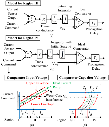
This model class is characterized by four regions, which can be observed in Fig. 19(c). Region I is the “blanking” region, where large and very fast but quickly decaying switching transients dominate the current sensor output. It is worth noting that in the many instances that this region is blanked, the blanking occurs after the output of the comparator to defer the peak current event detection. Region II is the “subthreshold” region where the worst-case current sensor waveform is below the current command. Region III is the “threshold” region where the current sensor waveforms are neither unambiguously below nor above the current-command threshold; in this region, the waveform can cross the threshold multiple times. Region IV is the “overdrive” region where the current sensor waveform is always above the current command. The qualifying restriction on Region II, III, and IV for this model class is that waveform is never below the minimum current command.
In Regions I and II, we consider the comparator capacitor remaining in reset or equivalently, negatively saturated. In Regions III and IV, the capacitor integrates the current that is representative of the difference between the current command and the current sensor output; the mathematical formalization requires two different types of integrators to describe each region, as shown in Fig. 19(a) and (b). The integrator resets every switching cycle for the usual case that the overdrive delay of the comparator is smaller than the minimum off time.
The ideal current sensor output (without interference) is a ramp, which crosses the current command threshold at . After , begins integrating; for the ideal current ramp, the capacitor voltage is a quadratic. When the capacitor voltage crosses the trigger voltage at , which results from a combination of the gains and MOSFET thresholds (for example in Fig. 16 for ), the comparator output changes state at . The overdrive delay is from to .
The current sensor output with interference in our model class can be bounded from above by an upper envelope and from below by a lower envelope in Regions II and III. The upper envelope crosses the current command earlier than the ideal current ramp by . The lower envelope crosses the current command later than the ideal current ramp by . The upper and lower envelope have the same comparator overdrive delay as the ideal current ramp because these envelopes have the same slope as the ideal current ramp given the bounded amplitude assumption,
| (35) |
Although the overdrive delays are identical, the upper envelope triggers earlier than that of the ideal current ramp by and the lower envelope triggers later by .
The worst-case interference waveform that can be contained by the upper and lower envelopes is a trapezoidal signal [11]. The lower bound of the interference frequency is the fundamental of the trapezoidal signal. The largest slew rate of the trapezoidal signal is the upper bound of the Lipschitz constant .
Comparator overdrive conditioning decreases the trigger time deviation from the ideal ramp for waveforms within the envelope bounds. In Region III, the time deviation of the crossing event of the worst-case interference from that of the ideal current ramp can range from earlier to later. In Region IV, the capacitor voltage trajectory given the worst-case interference input is strictly bounded between the quadratic trajectories of the upper and lower envelope inputs. This is a strict bound because the integral of the worst-case trapezoid is bounded from above by ; hence, the comparator output cannot trigger earlier than nor later than . The tradeoff of this control conditioning method is that longer overdrive delay becomes commensurate with smaller trigger time deviation. This overdrive delay manifests as a limitation to an outer control loop, which might for example, control output voltage.

Delay and nonlinearity are the pertinent effects that determine stability and transient performance. Region I (blanking), Region II (subthreshold), and Region III (threshold) are modeled as pure delays in Fig. 19(c). is a constant that encapsulates the circuit delays that are independent of the comparator input. This model for comparator overdrive delay agrees well with the real-world data [12] shown in Fig. 20(a) and Fig. 20(b).
The model for Region III (threshold) is shown in Fig. 19(a). The salient feature of this model is the saturating integrator, whose state and hence output is bounded both from above and below, but behaves like a linear integrator between these bounds. An implementation of a comparator with this behavior is illustrated in Fig. 16, where is always above ground. It is worth noting that the comparator circuit actually possesses this behavior in all four of the the model regions. Stability guarantees can be proven by partitioning the comparator behavior into these regions and restricting the saturating integrator behavior to Region III.
This saturating integrator behavior is mathematically important in that the saturating integrator is a sublinear function, which enables the proof of continuity in the static mapping [6]. STOP The behavior in Region III be represented by
| (36) |
We define as the last instant in Region III when the output of the integrator is zero.33 3 We provide a short proof for this statement: the saturating integrator always has positive or zero state at any threshold crossing instants. We start from the last instant and backwards check the integrator states at each threshold crossing instants. We stop at the instant at which the integrator state is zero. This algorithm is guaranteed to stop because the integrator state must be zero at the first threshold crossing instant. Therefore, the stop instant is the we want.
| (37) |
After , the behavior in Region III is a linear integrator with a voltage output at the end of Region III
| (38) |
The model for Region IV (overdrive), which represents a strictly positive integrator output is modeled in Fig. 19(b). The initial output of the integrator embeds the saturating integrator behavior in Region III. is bounded from above by , which is induced by the upper envelope of the current sensor output. is bounded from below by the lower bound of the saturating integrator.
The comparator overdrive in Region IV can be represented by
| (39) |
In (39), represents the error between the current sensor output and the current command.
By substituting (38) into (39), the comparator overdrive can be represented as
| (40) |
Together with the dynamics of the constant off-time current control loop, the system using the comparator overdrive can be represented as
| (41a) | ||||
| (41b) | ||||
where the comparator time constant is the design variable for comparator-overdrive-delay conditioning. Equation (41a) describes the feedback path and (41b) describes the forward path.
Proposition 1 in the Part I of the paper [8] states that if the current sensor output is not monotonic, then the static current mapping is discontinuous. A discontinuous static mapping can make the current control loop unstable. We use as the metric for the comparator overdrive delay. Theorem 3 below states that an appropriately designed comparator overdrive delay can make the static mapping continuous. Figure 20(c) demonstrates Theorem 3 by plotting three static mappings with different comparator overdrive delays. We observe that given small , the static mapping is discontinuous. As we increase , the degree of discontinuity of the static mapping decreases. The static mapping becomes continuous if is large enough. Mathematically, the degree of discontinuity can be defined as the Lebesgue measure on the set of unreachable points.
Theorem 3.
Given a constant off-time current control loop with comparator overdrive delay, if the input is a ramp with slope and interference function , the condition to guarantee the continuous static current mapping is
| (42) |
Having satisfied the condition of continuous static mapping, we next show that the comparator overdrive delay allows the dynamical mapping to be stabilized. Comparator overdrive conditioning attenuates the effect of interference by averaging, hence its performance improves with increasing interference frequency. The averaging time interval is determined by ; smaller results in longer averaging time and hence a better interference attenuation. Smaller contributes to a bigger delay, which means that interference attenuation trades off with transient performance. Theorem 4 describes the stability constraint on the design of ; Theorem 5 describes the constraint from the hardware limits on minimum on time.
Theorem 4 shows there exists a minimum comparator time constant, above which the current control loop is guaranteed to be globally asymptotically stable. The stability of the dynamical mapping depends on the upper bound of the interference amplitude and the lower bound of the interference frequency . Only a short overdrive delay is needed to stabilize the current control for small and large . This is consistent with the behavior we described in Fig. 19.
Theorem 4.
Given a constant off-time current control loop with comparator overdrive delay, if the input is a ramp with slope and interference function , the condition to guarantee a globally asymptotically stable dynamical mapping is
| (43) |
where
The proof of this Theorem is based on the observation that (41a) is an implicit nonlinear function from to the deviation of peak current . Therefore, the current-control loop can be represented as a Lure system. Equation (41b) describes the linear forward path and can be found in (21). (41a) describes the nonlinear feedback path and is sector-bounded. The detailed proof can be found in [6]. Equation (43) shows that a current control loop with large interference amplitude can be stabilized by a comparator with a large time constant .
However, having a time constant that is too large results in an overdrive delay that may be too long. Long overdrive delay increases the minimum on time of the current control loop, hence slowing down transient response. Theorem 5 shows a rigorous upper bound on the overdrive delay.
Theorem 5.
Given a constant off-time current control loop with comparator overdrive delay, if the input is a ramp with slope and interference function , the maximum comparator overdrive delay is
| (44) |
where
The maximum comparator overdrive delay depends on the interference, hardware parameters, and design variable . The proof can be found in [6].
The large-signal transient performance of the power converter is determined by the inductor current slew rate, which in turn is determined by the minimum on time . is a design objective for comparator-overdrive-delay conditioning. We design the comparator so that is as small as possible while maintaining stability. Therefore, a judicious choice is to design the longest overdrive delay to equal the minimum on time
| (45) |
We define the normalized interference frequency as
| (46) |
the normalized interference amplitude as
| (47) |
the normalized comparator time constant as
| (48) |
and the normalized minimum on time as
| (49) |
The base value for the normalization were chosen to be the operating points in the steady state. For example, represents the on time of the current control loop in the steady state.
We can acquire more intuition on the stability of the current control loop with comparator-overdrive-delay conditioning through linearization. The linearized model can be expressed as a block diagram in Fig. 21 with the linear feedback gain
| (50) |
where is the steady-state value of (37) and is the on time in the steady state.
Interference manifests in the feedback gain . Negative results in positive feedback and may destabilize the current control loop. Larger comparator time constant results in longer delay from to . From (50), larger can decrease the amplitude of and stabilize the current control loop. However, either positive or negative feedback can result in stable control loop.
We can visualize the stabilizing effect of comparator-overdrive-delay conditioning through the root locus, which is shown in Fig. 22. We observe that comparator-overdrive-delay for positive feedback in Figs. 22 (a) and (b) move the location of the worst-case closed-loop pole further to the right, hence improving stability margin. Likewise, for negative feedback in Figs. 22 (c) and (d), the closed-loop pole moves further to the left. In this way, comparator-overdrive-delay conditioning can guarantee that the closed-loop poles stay inside the unit disk, hence guaranteeing stability.
We next show the quantitative relationship between interference and the location of closed-loop pole. From (II-B), the closed-loop transfer function is
| (51) |
where
| (52) |
is defined in (50). Given an interference with amplitude upper bound and frequency lower bound , is bounded within the range where
| (53) |
The detailed derivations can be found in [6]. For different operating points, the pole is always real and within the range where
| (54) |
The condition for small-signal stability is
| (55) |
The worst-case settling and overshoot can be obtained from (28) and (29), respectively.


Figures 23(a), 23(b), and 23(c) show how the settling, overshoot and overdrive delay change with the comparator time constant. We observe that both the settling and overshoot decrease as comparator time constant increases; also, overdrive delay increases as increases. These observations match our intuition because the increase in the comparator time constant results in a corresponding increase in the ability of the comparator to attenuate interference; hence, overshoot and settling is smaller. However, with this increase in comparator time constant, overdrive delay is longer, in consequence sacrificing large-signal speed.
The analysis in this section can be used for control conditioning fixed-frequency peak current-mode control by substituting in (21) by (56).
| (56) | ||||
| (57) |
To extend the analysis to the constant on-time control or the fixed-frequency valley current-mode control, we need to substitute by and by in (46) and (47).
In summary, comparator-overdrive-delay conditioning can be a powerful control conditioning approach that can be easily implemented. The analog comparator, which is commonly used in peak current-mode control, can directly have a dual-use as an interference attenuator without extra complexity. Within an integrated circuit, the level of attenuation can be easily chosen by adjusting the tail current.
III Hardware Results
We use a multi-megahertz buck converter prototype as a working hardware example to demonstrate the effectiveness of control conditioning for current control loops with interference dysfunction. For this prototype, we selected constant on-time current-mode control, which is frequently used in high-speed converters for microprocessors. The schematic is shown in Fig. 24.
III-A DC-DC Converter Hardware Prototype Platform
The conditioning methods in this paper apply for alleviating the effect of interference that occurs in all types of current sensors. We employ the ground-referenced shunt-resistor current sensor as a widely-used exemplar because of its simplicity and wide measurement bandwidth. A 5 MHz buck converter demonstrating cycle-by-cycle control is specified in Table I. This constant on-time current mode converter delivers 2 V at 30 Watts from a 12 V input.
The control algorithms were implemented in a low cost Xilinx Artix-7 FPGA together with a 15 MHz high-speed ADC and a 40 MHz DAC are used in the digital system. The FPGA communicates with the ADC through a 100 MHz LVDS high-speed interface. We implemented a hybrid digital and analog controller for current-mode control with commercial off-the-shelf comparators. The hardware is shown in Fig. 25.
| Parameters | Values | Parameters | Values |
|---|---|---|---|
| 12 V | 240 nH | ||
| 2 V | 0.2 | ||
| 8 A | 10 m | ||
| 100 ns | 5 MHz | ||
| 100 F | 4 mV |

III-B Comparing the Three Control Conditioning Methods


Slope compensation, low-pass filtering, and comparator-overdrive-delay conditioning repair corrupted static and dynamical mappings. From a unified framework, we compare these three control conditioning methods. All three methods decrease the degree of nonlinearity in the static mapping, but introduce other non-idealities that must be addressed. Low-pass filtering repairs the nonlinearity caused by the interference, but introduces its own nonlinearity in the current sensor output; these two nonlinearities must be balanced to minimize the overall nonlinearity. Slope compensation adds a gain error while comparator-overdrive-delay conditioning causes an offset error in the static mapping. All three methods ensure stability and improve transient response of the current control loops. To compare control-conditioning methods, we use overshoot and settling as performance metrics.
It is inadequate to compare either the settling or overshoot in isolation because each method allows designers to trade-off between these two performance metrics through design parameters. Instead, we compare among the tradeoff spaces and construct two-dimensional performance spaces as shown in Figs. 26(a) and 26(b). By varying the key design parameter for each method, e.g. compensation slope, filter time constant, or comparator time constant, we plot the point set for each of the three methods in this space. One observes that the points closer to the origin have a better performance tradeoff in overshoot and settling. These curves depend on the interference parameters , with all methods performing worse with higher interference amplitude. We define as the interference frequency band, which means the set of frequencies within which the interference frequency is contained. In this paper, the interference frequency refers to the interference frequency band.
Fig. 26(a) illustrates that if switching frequency is much lower than the interference frequency (e.g., ), both the comparator-overdrive-delay conditioning and low-pass filter achieve a smaller overshoot and shorter settling than slope compensation. Fig. 26(b) illustrates that if the switching frequency is comparable to the interference frequency (e.g., ), comparator overdrive-delay-conditioning and slope compensation result in a smaller overshoot and shorter settling than the low-pass filter. For comparator-overdrive-delay conditioning, both the overshoot and settling monotonically increase together. However, because the reduction of overshoot and settling is effected by increasing the comparator overdrive delay, the minimum on time is also increased. It is worth noting that this is so because the minimum on time is equal to comparator overdrive delay, i.e. the decision to turn the switch off cannot be made before the comparator can output its comparison. This minimum on time saturation has consequences in the large signal design of the overall power converter control loop. A qualitative comparison of the three conditioning methods is summarized in Table II.
| Method | Less | Transient Performance | Transient Performance | |
| Complexity | @ | @ | ||
| Filter | +++ | ++ | + | |
| Slope Compensation | ++ | + | ++ | |
| Comparator Overdrive | + | +++ | +++ |
The transient performance of the filter is the best when the switching frequency is well below the interference frequency. When the switching frequency is within the range of the interference, both slope compensation and comparator-overdrive-delay conditioning perform well. However, comparator-overdrive-delay conditioning incurs a higher complexity when implemented discretely, but is much more straightforward within an integrated circuit; additionally, as mentioned above, the dependence on minimum on time adds an additional constraint. Adaptive tuning is straightforward for both slope compensation and comparator-overdrive-delay compensation.
III-C Control Conditioning Using Slope Compensation
We exhibit a digital slope generator with programmable slope in Fig. 27. The slope is programmed by the increment value register . The output of the digital controller determines the offset value of the valley current. The counter is triggered and reset every cycle. The constant-on-time modulator resets the counter to 0 at each rising edge and freezes the counter during the entire on time. The counter starts at the falling edge of the constant-on-time modulator and counts upwards. represents the summation of the valley current offset and slope . is converted into an analog signal by the DAC. The output of the DAC is updated at the rising edge of the DAC clock. The filter smooths the stepped so that it is nearly an ideal ramp. The digital slope generator and controller are implemented in the FPGA, and the DAC and filter are implemented in discrete hardware. This all-digital slope generator can be reconfigured in real-time to optimize for transient and stability at different operating points, in which gain scheduling is an example. All the critical waveforms can be found in Fig. 28.
The output of the slope generator can function correctly both in steady state and in transition as shown in Figs. 29(a) and 29(b). The slope generator output is shown in Channel 1 (dark blue). The inductor current is shown in channel 3 (pink) and the switching signal is shown in channel 2 (light blue). There is a propagation delay from the switching signal to the inductor current. We observe that the slope generator output is highly contaminated by the switch-on transient, but the slope compensation still functions correctly because we only need to compensate the current sensor slope during the off time, which means the switch-off transition does not induce heavy interference on the slope generator output.


Without slope compensation, the inductor current is not stable because of the contaminated current sense voltage as illustrated in Fig. 30(a). The subharmonic frequencies of one-fifth to fourth-fifths of the fundamental frequency appear in Fig. 31(a). With slope compensation of 10 As, the inductor current is stabilized despite the severe contamination on the current sensor voltage as shown in Fig. 30(b). The only remaining harmonics are positive integer multiples of the fundamental frequency as validated by the Fourier spectrum in Fig. 31(b).
The slope compensation results in a second-order response to the current control loop as illustrated in Fig. 32(a). The greater the compensation slope, the slower the transient response as shown in Fig. 32(b). The current control loop is unstable in hardware when the compensation slope is 0 A/s. When the slope is increased to 10 A/s, the current controller settles quickly to a stable equilibrium within several cycles. The ringing disappears when the slope is further increased to 20 A/s. However, the current transient takes longer to settle.


III-D Control Conditioning Using Low-Pass Filter
We use the first-order low-pass filter for illustration. The design of the low-pass filter includes the design of time constant .


The constant on-time buck prototype is used as a hardware design example. Figures 33(a), 33(b), and 33(c) show the experimental waveforms of the current-mode buck converter with different conditioning filters. We vary the capacitor value to change the time constant of the first-order low-pass filter. The inductor current is shown in Channel 3 (pink) and the current sensor output is shown in Channel 1 (dark blue), which is highly contaminated by interference. Note that the filter capacitor pF is always placed at the comparator input, not only for low-pass filter conditioning, but also for slope compensation and comparator-overdrive-delay conditioning because it can condition the voltage spike during switching transients, in other words, limit the bandwidth of the current-sense output. This design not only protects the comparator from being overdriven, but also makes the assumption that the bandwidth limit holds in Definition 2 in the Part I of this paper [8].
If only the bandwidth limiting filter is used without proper design, the converter cannot function properly because inductor current exhibits a complicated subharmonic behavior as shown in Fig. 33(a). From the Fourier transform of inductor current in Fig. 34(a), we observe that in addition to the switching frequency component, the , , , and -order subharmonics are also commingled because of the interference. We increase the time constant of low-pass filter by increasing the capacitance to 22 pF. As shown in Fig. 33(b), the inductor current goes back to stable periodic steady state; Fig. 34(b), a longer-horizon view, further confirms our observation. The Fourier transform of inductor current only contains switching-frequency and higher-order harmonics. A further step to increase the capacitance to 68 pF destabilizes the inductor current as shown in Fig. 33(c). Figure 34(c) shows that unlike Fig. 33(a), the unstable inductor current in Fig. 33(c) only contains the order subharmonics. Experimentally, the steady state of the current control loop matches the theory. A fast filter cannot condition the interference and hence cannot decrease the nonlinearity of the static current mapping; a slow filter can distort the linear ramp and increase the nonlinearity.
The low-pass filter affects the transient response of the current control loop. We test the step-up response of the current control loop using four different low pass filters for control conditioning as shown in Fig. 35. For better illustration, we export the oscilloscope data to Matlab and plot them in Fig. 36. The valley currents are traced as a step plot (in red) to emphasize that we are directly controlling the valley current in this buck converter using constant-on time control. Using pF results in an unstable steady state; however, the current control loop is stabilized when the filter capacitor is increased to pF. The tradeoff to stabilizing the loop is the incurrence of 10 cycles of settling. The settling transient is faster when the filter capacitor is increased to pF; however, there is a relatively large overshoot during transients, which can be explained by the zero in (26) introduced by the filter. When pF, the current control loop devolves into a 2-cycle subharmonic instability.
III-E Control Conditioning Using Comparator-Overdrive-Delay


A neuromorphic analogy to comparator-overdrive-delay conditioning is reminiscent of how integrate-and-fire neurons behave [13]. This behavior in the control conditioning framework as it pertains to current sensor interference was discussed in Section II-C.
The experimental results for the comparator-overdrive-delay conditioning in a buck converter prototype can be observed in Fig. 37. The current control loop using an LT1711 [12] whose comparator time constant is too small is unstable. The current control loop using AD8469 comparator [14], whose comparator time constant is high enough, is stable.
Figures 37(a) and 37(b) show the experimental waveforms of the current-mode buck converter with different comparator overdrive delays. The inductor current is shown in channel 3 (pink) and the current sensor output is shown in channel 1 (dark blue), which is highly contaminated by interference.
As discussed in Section I, subharmonics in the switching result in poor converter behavior. Fig. 37(a) shows the subharmonics when the comparator overdrive delay is too small. From the Fourier transform of the inductor current, we observe that in addition to the switching frequency, the , , , -order subharmonics are also commingled because of the interference. Comparator overdrive delay can be increased using a different comparator; as shown in Fig. 37(b), the inductor current becomes stable in the periodic steady state. When stable, the Fourier transform of the inductor current only contains switching-frequency and higher-order harmonics.
From the experimental data, the steady state behavior of the current control loop agrees with the theory. A slow comparator can condition the interference and reduce the nonlinearity of current mapping so that the current loop is stable.
IV Conclusion
In this paper, we presented the analysis and design of three control conditioning methods for extremum current-mode controllers in high-frequency converters with disruptive current sensor interference. We provided a rigorous model for the dynamics of the current loop using these conditioning methods with interference, to ensure robust stability. Specifically, we compared and rigorously analyzed: (1) comparator overdrive delay conditioning; (2) slope compensation; and (3) low-pass filter conditioning, within the unified framework in Part 1 of this paper series. We experimentally demonstrated and validated in a multi-MHz power converter hardware the effectiveness of all three methods where interference was harsh.
Acknowledgements
Special thanks to Professor Peter Seiler for the contribution in large-signal stability analysis. This work is based upon work supported by the U.S. Department of Energy SunShot Initiative, under Award Number(s) DE-EE-0007549.
Appendix A Small-Signal Model of Current Control Loop with Time-Varying Inductor Current Ramp
If the coupling between the output capacitor voltage and inductor current ripple is not negligible, the small-signal model of current control loop with time-varying inductor current ramp follows:
| (58) |
where
Appendix B Considerations for Designing a Voltage Controller Around the Current Control Loop
A current-mode voltage converter has a major loop to control the output voltage and a minor loop to control the current. Although current control loop is the main topic of this paper, the design of the voltage controller depends on the design of the current control loop. To design the voltage controller , we need a model for the converter plant . The 5S framework in [5] provides a purely digital, simple and accurate model for this type of power converter.
| (59) |
where
| (60) |
Given the plant and current control loop in this section, the designer can design the voltage controller using the root-locus method in [15]. For other power converters like dc-dc converters using fixed-frequency control, the plant model is provided in Appendix C.
Appendix C Sampled-Data Space Modeling of a DC-DC Converter Using Fixed-Frequency Peak Current-Mode Control
We take the boost converter using fixed-frequency current-mode control with parameters as an example. The model is derived by following the sampled-data modeling method in [16] as:
| (61) |
where
| (62) | ||||
| (63) | ||||
| (64) | ||||
| (65) |
References
- [1] N. Yan, X. Ruan, and X. Li, “A general approach to sampled-data modeling for ripple-based control part I: Peak/valley current mode and peak/valley voltage mode,” IEEE Transactions on Power Electronics, pp. 1–1, Dec. 2021.
- [2] C. Bao, S. Guptam, and S. K. Mazumder, “Modeling and analysis of peak-current-controlled differential mode Ćuk inverter,” Proceedings of the 2021 IEEE 12th International Symposium on Power Electronics for Distributed Generation Systems, PEDG 2021, Jun. 2021.
- [3] N. Yan, X. Ruan, and X. Li, “A general approach to sampled-data modeling for ripple-based control part II: Constant on-time and constant off-time control,” IEEE Transactions on Power Electronics, pp. 1–1, Dec. 2021.
- [4] X. Zhang, Z. Zhang, H. Bao, B. Bao, and X. Qu, “Stability effect of control weight on multiloop COT-controlled buck converter with pi compensator and small output capacitor ESR,” IEEE Journal of Emerging and Selected Topics in Power Electronics, vol. 9, no. 4, pp. 4658–4667, Aug. 2021.
- [5] X. Cui and A.-T. Avestruz, “A new framework for cycle-by-cycle digital control of megahertz-range variable frequency buck converters,” in 2018 IEEE 19th Workshop on Control and Modeling for Power Electronics (COMPEL), Padova, 2018, pp. 1–8.
- [6] ——, “A note on comparator-overdrive-delay conditioning for current-mode control,” 2022. [Online]. Available: https://tinyurl.com/yv986ps6
- [7] ——, “A note on low-pass filter conditioning for current-mode control,” 2022. [Online]. Available: https://tinyurl.com/ydj5hbma
- [8] ——, “Overcoming high frequency limitations of current-mode control using a control conditioning approach - part i: Modeling and analysis,” arXiv, 2022.
- [9] R. Redl and I. Novak, “Instabilities in current-mode controlled switching voltage regulators,” in 1981 IEEE Annual Power Electronics Specialists Conference, 1981, pp. 17–28.
- [10] B. Razavi, Design of Analog CMOS Integrated Circuits. Tata McGraw-Hill Education, 2002.
- [11] Y. Katznelson, An Introduction to Harmonic Analysis. Cambridge University Press, 2004.
- [12] Linear Technology, “Lt1711 single/dual 4.5ns, 3v/5v/±5v, rail-to-rail comparators,” Tech. Rep., 2001.
- [13] W. Gerstner, W. M. Kistler, R. Naud, and L. Paninski, Neuronal dynamics: From single neurons to networks and models of cognition. Cambridge University Press, 2014.
- [14] Analog Device, “Ad8469 fast, rail-to-rail, low power, 2.5 v to 5.5 v, single-supply ttl/cmos comparator,” Tech. Rep., 2012.
- [15] X. Cui, C. Keller, and A.-T. Avestruz, “Cycle-by-cycle digital control of a multi-megahertz variable-frequency boost converter for automatic power control of lidar,” in 2019 IEEE Energy Conversion Congress and Exposition (ECCE), Baltimore, 2019, pp. 702–711.
- [16] G. Verghese, C. Bruzos, and K. Mahabir, “Averaged and sampled-data models for current mode control: a re-examination,” 20th Annual IEEE Power Electronics Specialists Conference, pp. 484–491, 2003.