Multi-scale time-resolved electron diffraction: A case study in moiré materials
Abstract
Ultrafast-optical-pump — structural-probe measurements, including ultrafast electron and x-ray scattering, provide direct experimental access to the fundamental timescales of atomic motion, and are thus foundational techniques for studying matter out of equilibrium. High-performance detectors are needed in scattering experiments to obtain maximum scientific value from every probe particle. We deploy a hybrid pixel array direct electron detector to perform ultrafast electron diffraction experiments on a WSe2/MoSe2 2D heterobilayer, resolving the weak features of diffuse scattering and moiré superlattice structure without saturating the zero order peak. Enabled by the detector’s high frame rate, we show that a chopping technique provides diffraction difference images with signal-to-noise at the shot noise limit. Finally, we demonstrate that a fast detector frame rate coupled with a high repetition rate probe can provide continuous time resolution from femtoseconds to seconds, enabling us to perform a scanning ultrafast electron diffraction experiment that maps thermal transport in WSe2/MoSe2 and resolves distinct diffusion mechanisms in space and time.
I Introduction
Ultrafast x-ray and electron scattering experiments are essential tools in the materials-by-design thrust of modern condensed matter physics and engineering, as they can probe far-from-equilibrium dynamic phenomena at atomic space and time scales Ihee et al. 2001; Cavalleri et al. 2001; Siwick et al. 2003; Gedik et al. 2007; Stojchevska et al. 2014; Sie et al. 2019. In this discipline, technological improvements in probe quality (space/momentum and time/energy resolution) and probe detection (sensitivity, speed) are key to enabling the discovery of new non-equilibrium material functionality Broholm et al. 2016; Carini et al. 2012.
Atomically thin moiré materials, such as twisted homobilayers or heterobilayers Cao et al. 2018; Yoo et al. 2019; Liao et al. 2020; Liu et al. 2020; Kim et al. 2021; Zhao et al. 2021; Gadelha et al. 2021, present exciting opportunities for ultrafast study given the wide array of equilibrium quantum phenomena observed in these systems, including superconductivity and orbital magnetism, that are tunable with twist angle Basov et al. 2017; Andrei et al. 2021. Appropriately tuned ultrafast excitation may be a route to optical switching of these properties, as has been observed in other quantum materials Fausti et al. 2011; Sie et al. 2019.
Many of the properties that make 2D materials physically interesting also pose significant challenges for ultrafast structural probes. Atomically thin films are inherently weak scatterers and this challenge is compounded by the fact that compact ultrafast probes generally offer lower time-average flux than their non-time-resolved counterparts Weathersby et al. 2015; Feist et al. 2017; Li et al. 2020. Further, important features in the information-rich diffraction patterns from these materials can be separated by many orders of magnitude in intensity: descending from the (0,0,0) peak, to Bragg scattering, to weaker satellite peaks caused by longer wavelength periodic lattice distortions (PLD), to yet weaker thermal diffuse scattering (TDS) Britt et al. 2022. In pump–probe ultrafast electron diffraction (UED), we seek to measure small changes in this already weak scattering. For example, important details of electron–phonon coupling can be found in parts per thousand modulation of scattering signals that in static diffraction are already at the level of total beam current. Moiré materials exemplify this challenge, and could plausibly present correlated signatures of interlayer interactions in Bragg, PLD and TDS scattering, with tunable superstructure periodicity that can extend to tens of Yoo et al. 2019.

To meet the material-science need to investigate ultrafast evolution of diffraction features across multiple intensity and length scales simultaneously – in the same scattering data set and with Poisson-limited experimental precision – requires bright probe sources and detectors with single-particle sensitivity and high dynamic range. Workhorse indirect detectors function by detecting light generated in a scintillator, which places limits on dynamic range, spatial resolution, and sensitivity R. Meyer and Kirkland 1998; Fan and Ellisman 2000; Zuo 2000; Gruner et al. 2002. The standard metric for detector performance is detective quantum efficiency (DQE): state-of-the-art indirect detectors offer DQE at best in the few tens of percent, whereas a purely shot noise limited detection system would have a DQE of unity Ruskin et al. 2013. Among devices that aim to overcome these limitations Vecchione et al. 2017, direct detectors are now an established tool at x-ray user facilities Allahgholi et al. 2019; Leonarski et al. 2018; Tate et al. 2013, and enable computational imaging with state-of-the-art resolution in non-time-resolved electron microscopy Jiang et al. 2018; Chen et al. 2021, higher energy resolution in electron-energy-loss spectroscopy Hart et al. 2017, and higher spatial-resolution in electron cryo-microscopy Shen 2018.
The most common approach to direct electron detection is pulse counting Faruqi and Henderson 2007, which saturates at one particle per pixel per relaxation period (order 100 ns) and thus cannot handle the large peak currents typical of UED experiments Weathersby et al. 2015. Integrating direct detectors, by comparison, accurately report the total probe-particle energy incident on each pixel and are uniquely suited for applications with high-intensity pulsed beams of sub- duration, such as UED Lee et al. 2017.
The direct electron detector we employ in this work, the Electron Microscope Pixel Array Detector (EMPAD) has a DQE (at zero spatial frequency) of 0.95, with a signal to noise ratio for individual electron detection approaching 100 for 140 keV electrons. Its novel in-pixel, hybrid analog/digital circuitry simultaneously provides very high dynamic range, as described below Tate et al. 2016.
Fluctuations in the probe current incident on the sample also limit precision when measuring scattering rates, even if the detector counts scattered particles perfectly. Causes include variation in laser power on the photocathode, changes in the quantum efficiency of the photocathode, and – critical in micro-diffraction – unavoidable jitter and drift in the probe beam position on the probe defining aperture. Fluctuations in probe current fail to oscillate around a time-independent mean: thus, experimental precision does not improve from simply averaging longer acquisitions.
Instead, the incident probe current often exhibits universal frequency dependence. The impact is severe when probing both real-space and reciprocal space features of the sample, as done in micro-diffraction experiments Li et al. 2022; Shen et al. 2018. In optical pump–probe modalities, such as absorption spectroscopy, high-frequency pulse chopping and lock-in detection is an essential technique that reduces frequency-dependent noise Schriever et al. 2008, but impossible to adopt in UED without a fast frame rate detector capable of measuring the reference signal at frequencies well above those of the noise sources.
Ultimately, sample lifetime under the stress of repeated pump–probe cycles imposes a physical bound on total experiment time. Therefore, reducing acquisition time by eliminating sources of noise (other than fundamental Poisson uncertainty) significantly increases the breadth of feasible pump–probe experiments.
Here we deploy the EMPAD integrating electron detector, with our high brightness keV ultrafast electron micro-diffraction beamline Li et al. 2022, to probe the out-of-equilibrium dynamics of a WSe2/MoSe2 moiré bilayer at long spatial periodicity (high resolution in reciprocal space) and ultrafast time scales Tate et al. 2016; Li et al. 2022; Bai et al. 2020; Wang et al. 2021. For the first time in UED, we resolve a periodic moiré superlattice Adrian et al. 2016. We integrate the superlattice signal without saturating the more intense Bragg peaks caused by angstrom scale interatomic spacing. We demonstrate that the detector frame rate enables a fast pulse chopping technique that drastically improves signal-to-noise in measurements of the sample response to ultrafast pumping.
The fast detector frame rate also enables a novel pulse-picking technique, which extends the range of timescales accessible in ultrafast pump–probe experiments beyond with precision. Implementations of pump–probe delays at the scale typically rely on electrical triggering, e.g., nanosecond Q-switched lasers or gain-switched diodes with picosecond pulse duration Domke et al. 2012. Femtosecond pulses, by increasing the peak laser field strength for the same deposited energy, have the potential to unlock interesting metastable behavior Disa et al. 2020, and our method could resolve, e.g., frequency modulations after excitation. We demonstrate our pulse-picking technique with a micro-diffraction probe and map the diffusion of heat in our sample in space and time from initial ultrafast excitation, out to thermal relaxation, with spatial resolution. Experimental access to timescales allows us to extract from our space-and-time-resolved data the thermal diffusivity of our moiré sample.
II Results
II.1 Resolving moiré superstructure
Our beamline setup is summarized in Fig. 1 and Appendix A; additional details can be found in a previous work Li et al. 2022. To take best advantage of the detector frame rate, we independently gate pump and probe pulse trains obtained from a femtosecond fiber-laser source with a repetition rate of . The pump wavelength in the experiments reported here is . In micro-diffraction mode, depending on the beam coherence required to resolve the reciprocal space structure of interest, typical charges per pulse on target range from 10 to 1000 electrons.
A magnetic quadrupole lens triplet controls the angular magnification of the diffraction pattern on the detector. Lens settings are summarized by camera length: the hypothetical drift distance to the detector plane that would result in equivalent diffraction data.
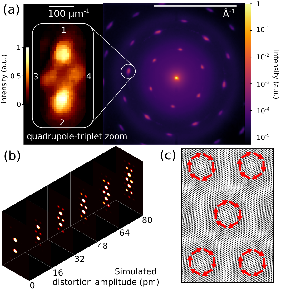
Figure 2(a) shows a static diffraction pattern obtained from the sample at short camera length. The six-fold symmetry of the diffraction pattern arises from the underlying symmetry of the lattices. The logarithmic scale color bar includes over four orders of magnitude of contrast from the (0,0,0) peak to thermal diffuse scattering.
The EMPAD consists of a grid of pixels each 150 in size. Each pixel has a thick reverse-biased silicon diode bump bonded to its own read-out electronic circuit. The well of each pixel can record up to electron incidents per exposure, but the detector saturates at lower counts if the rate of incidents exceeds a threshold. Previous measurements performed with continuous beam illumination (cw) estimated this threshold rate to be electrons per pixel per microsecond at our beam energy. Surprisingly, in our pulsed experiments we observe saturation at the significantly higher rate of 60 electrons per pixel per sub-picosecond pulse, a result likely analogous to effects studied in the context of x-ray free electron laser applications, and discussed further in Appendix B. The EMPAD design is under active development and the latest iteration (not deployed in our experiments) increases the cw saturation level to electrons per pixel per microsecond Philipp et al. 2022.
The inset to Fig. 2(a) shows a long-camera-length diffraction difference pattern isolating a single pair of Bragg peaks , aligned vertically in the image, with two additional satellite peaks visible, aligned horizontally. The difference pattern is formed by subtracting pumped exposures from unpumped at a delay of 4 ps. In an unpumped diffraction pattern, the more intense of the two highlighted Bragg peaks results from scattering off the monolayer, the other from the monolayer. The reverse is true of the pumped difference image inset to Fig. 2(a): the more intense peak results from the stronger response of the layer. The interlayer twist angle controls the separation in reciprocal space between the two Bragg peaks, measured here to be .
The sixfold symmetry of the real-space moiré pattern entails that scattering from the moiré superlattice forms a hexagon dressing each Bragg peak. The satellites observable in the inset to Fig. 2(a) lie at scattering vectors where monolayer contributions overlap. Static selected area electron diffraction (SAED) from twisted bilayer graphene performed by others shows that the intensity of moiré satellite peaks decays exponentially with twist angle between – Yoo et al. 2019. These results, and static SAED data from twisted Kim et al. 2022, are consistent with our observation of two satellites along the midline of a Bragg pair. Interlayer interactions strain the monolayers: simulated diffraction patterns presented in Fig. 2(b) show that satellite peaks are absent without this strain and grow in intensity as strain increases (see Appendix D for simulation details). A future work will present time-series data showing the detailed dynamics of the moiré superstructure.
II.2 Reaching Poisson-limited experimental uncertainty
In this section, we demonstrate with experimental data how fast beam chopping coupled with high detector frame rate dramatically improves signal to noise in ultrafast pump–probe experiments. The chopping concept is illustrated in Fig. 3. To put the results of this section in context, it is necessary to briefly summarize the relevant sources of noise. The typical signal in UED is the fractional change in scattering intensity as a function of delay time and scattering angle. Distinguishing pumped exposures, when the pump beam is incident on the sample, from unpumped exposures, when the pump beam is off, can be expressed in terms of the ratio of the number of scattered electrons within a given solid angle to the number of incident electrons:
| (1) |
where the additional subscript or corresponds to the pumped or unpumped condition. The contribution of the probe beam to total experimental uncertainty in estimating is then analyzed by considering contributions from each appearing in Eq. (1). These contributions are conveniently aggregated into four terms Kealhofer et al. 2015:
| (2) |
Each term in Eq. (2) corresponds to elements that together comprise the entire scattering experiment: accounts for the Poisson distribution in the number of electron scattering events; accounts for uncertainty introduced in converting electron incidence into detector counts; finally, and account for uncertainty introduced in emitting and transporting electrons from source to detector. As the relative importance of each term depends on signal intensity Kealhofer et al. 2015, all four can be important in an experiment that aims to resolve diffraction features at separated intensity scales simultaneously.
The shot noise contribution to is dominated by the contribution from scattered electrons, so that:
| (3) |
As a numerical illustration, to resolve a 1% change in a diffraction feature intensity with 0.5% rms uncertainty requires a minimum of electrons scattered into that feature. The corresponding minimum accumulation time, supposing a high charge machine with electrons per pulse at a repetition rate Britt et al. 2022, and scattering factor, is only . Nonetheless, stroboscopic UED experiments often integrate for much longer to achieve this same level of experimental uncertainty (e.g., Britt et al. 2022; Chase et al. 2016; Yang et al. 2020), because in these experiments is not the most significant term in .
Contributions to depend on the detector technology, and include per count amplification noise as well as readout noise Kealhofer et al. 2015. With respect to the EMPAD, rms read noise (where the average is taken over all pixels) is equivalent to 0.011 electrons at , a signal-to-noise of 100. Weiss et al. 2017.
The final two terms in Eq. (2), and , are dominated by the contribution from incident electrons, which arises from loss of information about the incident beam. Significant loss of information occurs if the intensity of the beam at zero scattering angle is not recorded. Failure to record this information can occur because the beam at zero scattering angle saturates the dynamic range of the detector, but the EMPAD is not saturated in the micro-diffraction experiments we report here. Instead, in our high-momentum-resolution experiments at long camera length, e.g., the inset to Fig. 2(a), the 2 cm diameter of the pixel detector does not allow simultaneous sampling of the zero-angle peak together with the diffraction features of interest — the sidebands due to moiré interlayer interactions. This limitation could be overcome by combining multiple detectors into a larger array, as has been demonstrated with a version of the EMPAD in x-ray imaging Tate et al. 2013. Jitter and drift arising from electron transport are specific to the experimental setup and lab environment. With reference to our setup, a micron scale probe defining aperture in micro-diffraction mode makes the transmitted current sensitive (at the 0.1% – %1 level relevant in UED) to micro-radian changes in beam pointing. Kicks of this size are likely the result of integrating electromagnetic pollution (partially compensated by Helmholtz coils) along the 3 m distance from cathode to sample. Techniques to achieve electromagnetically, as well as mechanically, cleaner lab environments developed for atomic resolution scanning transmission microscopy could also be implemented to improve beam transport in micro-UED Muller et al. 2006.
Absent direct measurements, the number of incident electrons must be estimated from correlated information, for example, monitored photo-emission laser power and acquisition time Kealhofer et al. 2015. In our micro-diffraction experiment, these indirect sources of information cannot track fluctuations due to transport through our probe-defining aperture just upstream of the sample. Figure 4 shows a measured frequency spectrum of total current transmitted through our probe-defining aperture.

To demonstrate that beam chopping eliminates jitter and drift as sources of uncertainty in pump–probe experiments, Fig. 5(a) shows the measurement of the ultrafast response at two chopping frequencies with the small probe beam. The trend is an exponential decay convolved with the instrument response Chatelain et al. 2014. The non-zero sample response at delay times earlier than the pump arrival is due to thermal cycling, investigated below. Each data point is acquired with a two-minute integration time. The spread in the data at the slow chopping rate (one minute pumped, followed by one minute unpumped) is comparable to the size of the ultrafast effect. In stark contrast, the data acquired at the chopping frequency follows the fitted trend closely.
Further investigating the dependence of experimental uncertainty on beam-chopping frequency, we benchmark our experimental uncertainty with pump–probe time-series data, summarized in Fig. 5(b). We can estimate frequency dependence by taking averages with the respect to an ensemble of time-bins of variable duration . We compute a variance-to-mean ratio (VMR) as a function of :
| (4) |
where denotes the variance of over duration- time-bins and the mean over the same bins. The VMR defined in Eq. (4) can be interpreted as the square of the experimental uncertainty in estimating the effect of pumping the sample, normalized by the shot noise limit. If are drawn from independent Poisson distributions then the VMR must equal one. The VMR rises above one with the introduction of fluctuations in the mean of the Poisson distribution, due, e.g., to fluctuating laser power on the photocathode, and noise in the steering magnets and accelerating voltage.
Figure 5(b) plots (as defined in Eq. (4)) against chopping frequency and compares higher intensity Bragg scattering peaks with the 30% weaker superlattice peaks. The two data sets are fit to power law trend lines. Both data-sets are at the shot noise floor when chopped at . The data reveals that the higher the scattering rate, the higher the chopping frequency required to hit the shot noise floor (holding fixed the total integration time). At the higher scattering rate, the VMR is appreciably greater than unity at chopping frequencies below , while at the lower scattering rate, the VMR begins to rise above shot noise only below . The explanation is that more counts for fixed acquisition time reduces the Poisson contribution to the noise in any given frequency band, increasing the experimental sensitivity to jitter and drift in the same band. It follows that for fixed acquisition time the chopping frequency required to reach the shot noise floor depends both on the experimental setup – the average probe current – and on the intrinsic details of the scattering mechanism, e.g., low intensity thermal diffuse scattering is shot noise limited at a lower chopping frequency than high intensity Bragg scattering.
II.3 Scanning micro-diffraction in space and time
The ability to isolate and compare the response to excitation at and delays is critical to understanding microscopic heat transport and potentially the formation of meta-stable phases Fausti et al. 2011. The pulse-picking method illustrated in Fig. 1 allows us to perform multi-dimensional, multi-scale thermometry on via the Debye–Waller effect. The detector frame rate sets the effective repetition rate of the pulse-picked probe, so that the frame rate reduces the time required to perform the experiment from weeks with a conventional CCD to eight hours with the EMPAD.
Our multi-dimensional, multi-scale thermometry data is shown in Fig. 6. The three data dimensions are probe delay and probe position (both plotted horizontally) and the relative change in diffraction intensity (plotted vertically). Colors indicate which spatial cuts in Fig. 6(b) correspond to the pump–probe delay shown in Fig. 6(c). Panel (b) i. shows the ultrafast response taken at a pump delay of . The remaining data are taken by progressively extending the duration of the pump pulse train and probing the sample after the final pulse in the pump pulse train. The increment corresponds to the period between pulses at our repetition rate. The data in Fig. 6(b) ii.–v. clearly show the accumulation of energy through the duration of the pump pulse train, while panels vi.–viii. show the dissipation of energy to the sample boundaries after the pump-pulse train terminates.
In the limit that the relaxed sample temperature is well above zero and the temperature change is small, both compared to the sample Debye temperature, the fractional change in the Bragg scattering rate with scattering vector is proportional to . Hence, by scanning as a function of pump spatial position and pump delay, it is possible to map out thermal transport in the sample. We choose a low pump fluence of as a compromise between, on the one hand, maintaining linearity in the relationship between and , and on the other, minimizing Poisson noise in the diffraction difference.
To model the heat transport phenomenology, we fit to our diffraction signal to an analytic, approximate solution to the inhomogeneous 2D heat equation,
| (5) |
The periodic solution contains three parameters: the diffusion constant , and the amplitude and width of the pump pulses. The forcing term represents the pump injecting energy into the system. The model makes no assumptions concerning the transport mechanism. The diffraction intensity is the sum of peaks labeled 1–4 in Fig. 2(a). Eq. (5) is solvable by Fourier series, and we obtain an analytic approximation by simply truncating this series to finite order. The Supplemental Material provides a detailed derivation of the explicit expression.
We find excellent agreement between our data and three-parameter phenomenological model. Solid lines in Fig. 6(b) ii–viii show the spatial profile implied by the fitted model; the solid line in Fig. 6(c) shows the fitted temperature envelope at the center of the sample square. The interpretation of Fig. 6 is that the extreme aspect ratio of the bilayer–substrate combination – thick versus wide – results in two relaxation timescales: a fast timescale, , and a slow timescale, . The fit implies a decay in the temperature of the bilayer following the arrival of the first pump pulse to 5% of its peak value before the arrival of the second. This 5% residue accumulates for the duration of the pulse train and, following the end of the pulse train, relaxes exponentially at a rate set by the sample window size : .
The fit in Fig. 6 gives the value . When, as in our experiment, the period between pump pulse trains is less than the relaxation time, the bilayer reaches a periodic state in which the minimum temperature of the pumped region during a cycle remains elevated above the temperature of the boundaries. The estimate of unambiguously defines the repetition rate that allows for the sample to fully relax before the arrival of each pump pulse in stroboscopic data acquisition. This relaxation time is sample and substrate dependent, as are the physical implications of pumping at a repetition rate faster than sample relaxation. Our method of extending the range of ultrafast pump–probe delays to – enables us to investigate these issues experimentally.
Pump–probe delays in the – range provide a technique to extract the transverse thermal conductivity of the bilayer. This intrinsic property cannot be inferred from sub-ns data alone, because the ultrafast relaxation we observe is dominated by the interfacial resistance between bilayer and SiN substrate, as heat is transferred across the dimension Britt et al. 2022. Whereas, on the slow timescale, the bilayer and SiN substrate provide parallel channels for conducting heat transversely over the distance to the wafer at the transverse boundary.
The transverse diffusivity parameter that we fit with our phenomenological 2D model (solid lines in Fig. 6(b)–(c)) does not discriminate between bilayer and substrate contributions. From the same data, finite-element simulations (see, e.g., Zalden et al. 2019) can extract the intrinsic transverse diffusivity of the bilayer. We find close agreement between simulation and the approximate analytic relationship,
| (6) |
where , are the transverse diffusivity and heat capacity of the bilayer, , are the traverse diffusivity and heat capacity of the substrate, and is the transverse diffusivity of the bilayer–substrate combination that we measure experimentally.
Hypothetically, data obtained from a freestanding bilayer would be simpler to analyze: however, an implication of the data we collect is that pumping a freestanding bilayer with fluence at or faster repetition rates would cause irreversible damage within a few pulses, without the SiN present to act as a heatsink. In testing samples mounted on SiN, we observed an irreversible drop in scattering intensity at a fluence of . A scanning-micrograph recorded with our electron probe showed the damage to be localized to the region illuminated by the pump-laser spot, a conclusion confirmed by post-mortem optical microscope images of the sample. The ability to reach higher fluences reversibly is important because even reversible structural responses can change discontinuously as a function of fluence Sie et al. 2019, possibly because the out-of-equilibrium electron population excited by the pump undergoes a phase transition as a function of the density of excited charges — in the case of our sample from an excitonic to a free electron gas Wang et al. 2021. These fluence-dependent physical mechanisms cannot be fully explored in experiments where fluence is constrained by the sample environment.
III Discussion and Conclusion
This work has presented new, dramatic advantages of an integrating direct electron detector with high dynamic range and fast frame rate for structural dynamics data acquisition. We are able to resolve the ultrafast response of a periodic moiré superlattice, and to track the long thermal relaxation of the bilayer following ultrafast excitation. Future experiments plan to apply this technique to investigate the effects of interlayer interactions on thermal transport in two ways: by measuring the dependence of transverse relaxation on bilayer twist angle Wang et al. 2021, and by tuning pump photon energy to resonantly excite a specific monolayer in the heterostructure.
Our results show that beam chopping at frequencies up to eliminates experimental uncertainties that are caused by non-Poissonian fluctuations in the probe current on target. In micro-diffraction, an important non-Poissonian source of uncertainty is positioning error on the probe defining aperture. Beam chopping is especially important in experiments where detector saturation or limits on field of view (at fine angular resolution) preclude measuring the total charge on target per pulse. Beam chopping is a complement to techniques that eliminate time-of-arrival jitter as a source of experimental uncertainty Otto et al. 2017.
The next generation EMPAD increases the frame rate to Philipp et al. 2022, which raises the maximum chopping frequency. Our results suggest that chopping frequencies above , while unnecessary for our system in micro-diffraction mode (100 electrons on target per pulse) have the potential to significantly improve signal-to-noise in experiments that involve large bunch charges of electrons or more, and in high-flux x-ray experiments with free electron laser sources.
A natural extension of our pulse-picking technique is to utilize a commercially available femtosecond GHz oscillator and fast pulse picker to achieve nanosecond pulse selection precision prior to the amplification stage. Such a system, when coupled with a delay stage to cover the range , would provide seamless delay capability from femtoseconds to seconds with femtosecond resolution. Measuring the transverse relaxation time of the bilayer, we demonstrate an experimental method for unambiguously defining the sample-dependent optimal repetition-rate for ultrafast stroboscopic data collection. Our results highlight the need for pump–probe modalities that can access multiple time and intensity scales when investigating the rich, multi-scale physics of 2D quantum materials.
This work was supported by the U.S Department of Energy, awards DE-SC0020144 and DE-SC0017631, and U.S. National Science Foundation Grant PHY-1549132, the Center for Bright Beams. D.L., A.S., and A.M.L. acknowledge support from the U.S. Department of Energy, Office of Science, Basic Energy Sciences, Materials Sciences and Engineering Division, under Contract DE-AC02-76SF00515.
Appendix A MUltrafast Electron Diffaction
Our beamline is shown in Fig. 7(a). The probe electron beam is photoemitted with 650 nm laser pulses and accelerated to a primary energy of , and the sample is pumped with pulses obtained from the same source. Electron beam optics for magnifying the diffraction pattern are shown in Fig. 7(b). Our scanning ultrafast electron diffraction technique is illustrated in Fig. 1. The spot size of the electron probe on the sample is defined by a laser-milled aperture upstream. An in-vacuum lens focuses the pump pulse to a rms spot on the sample, and the pump spot is steered on the sample by an out-of-vacuum mirror. A virtual-sample camera placed out of vacuum monitors the location of the central peak of the pump laser to precision. The duty cycle of the acousto-optic modulator that gates pump pulses is variable to single-pulse precision: we typically choose a duty-cycle to match the detector exposure, eliminating un-detected pulses and thus reducing the thermal load on the sample. We verify the reliability of the timing system by measuring the total pump-energy per exposure with the detector, and we see a sharp quantization of energy as a function of exposure length at intervals of the laser repetition period. Pump and probe beams are aligned by performing knife-edge scans at the vertical and horizontal sample edges. For the data presented in main text Fig. 6, knife-edge scans give 6 rms probe size in the sample plane.

Appendix B Detector Saturation
We observe saturation at 60 incident electrons per pixel per pulse in pulsed operation at . We arrive at this experimental estimate by averaging single shot measurements, and controlling the charge per pulse by varying the charge transmitted through the probe-defining aperture. The maximum charge that the EMPAD can remove per charge-removal cycle per pixel is equivalent to 11 incident electrons at this beam energy. The maximum is set by protection diodes that limit the peak charging current of each pixel’s storage capacitor. There thus appears to be a discrepancy between, on the one hand, the saturation threshold we observe and, on the other, the limit set by the electronics. A plausible resolution of the discrepancy is this: the high charge density in pulsed operation results in the creation of an electron–hole plasma with microseconds lifetime. The long-lived plasma is removed over multiple charge-removal cycles Weiss et al. 2016. The charge-removal circuitry cycles at , the probe beam repetition rate is , and hence there are 16 charge removal cycles for every probe pulse.
Appendix C Sample Preparation
MoSe2 and WSe2 monolayers are exfoliated from bulk MoSe2 and WSe2 single crystals (HQ graphene) onto 285 nm substrate sequentially using a gold tape exfoliation technique Liu et al. 2020, forming heterostructures with lateral dimensions of mm scale. The crystal orientations of the monolayers in the heterostructure are aligned with the crystal edges, and further confirmed in electron diffraction. The heterostructures are later transferred onto 10 nm thick, 250 Si3N4 windows on TEM grids (SiMPore), using a wedging transfer technique with cellulose acetate butyrate (CAB) polymer Schneider et al. 2010.
Appendix D Diffraction simulation
Diffraction patterns in Fig. 2(b) are computed from the Fourier transform of the real-space phenomenological model presented in Zhang and Tadmor 2018. Retaining only the longest-wavelength components of the PLD, atomic positions are displaced by a spatially varying vector field with explicit expression,
| (D.1) |
where is the amplitude parameter and are the reciprocal lattice vectors of the moiré superlattice.
References
- Ihee et al. (2001) H. Ihee, V. A. Lobastov, U. M. Gomez, B. M. Goodson, R. Srinivasan, C.-Y. Ruan, and A. H. Zewail, Direct imaging of transient molecular structures with ultrafast diffraction, Science 291, 458 (2001).
- Cavalleri et al. (2001) A. Cavalleri, C. Tóth, C. W. Siders, J. A. Squier, F. Ráksi, P. Forget, and J. C. Kieffer, Femtosecond structural dynamics in during an ultrafast solid-solid phase transition, Phys. Rev. Lett. 87 (2001).
- Siwick et al. (2003) B. J. Siwick, J. R. Dwyer, R. E. Jordan, and R. J. D. Miller, An atomic-level view of melting using femtosecond electron diffraction, Science 302, 1382 (2003).
- Gedik et al. (2007) N. Gedik, D.-S. Yang, G. Logvenov, I. Bozovic, and A. H. Zewail, Nonequilibrium phase transitions in cuprates observed by ultrafast electron crystallography, Science 316, 425 (2007).
- Stojchevska et al. (2014) L. Stojchevska, I. Vaskivskyi, T. Mertelj, P. Kusar, D. Svetin, S. Brazovskii, and D. Mihailovic, Ultrafast switching to a stable hidden quantum state in an electronic crystal, Science 344, 177 (2014).
- Sie et al. (2019) E. J. Sie, C. M. Nyby, C. D. Pemmaraju, S. J. Park, X. Shen, J. Yang, M. C. Hoffmann, B. K. Ofori-Okai, R. Li, A. H. Reid, S. Weathersby, E. Mannebach, N. Finney, D. Rhodes, D. Chenet, A. Antony, L. Balicas, J. Hone, T. P. Devereaux, T. F. Heinz, X. Wang, and A. M. Lindenberg, An ultrafast symmetry switch in a Weyl semimetal, Nature 565, 61 (2019).
- Broholm et al. (2016) C. Broholm, I. Fisher, J. Moore, M. Murnane, A. Moreo, J. Tranquada, D. Basov, J. Freericks, M. Aronson, A. MacDonald, E. Fradkin, A. Yacoby, N. Samarth, S. Stemmer, L. Horton, J. Horwitz, J. Davenport, M. Graf, J. Krause, M. Pechan, K. Perry, J. Rhyne, A. Schwartz, T. Thiyagarajan, L. Yarris, and K. Runkles, Basic research needs workshop on quantum materials for energy relevant technology, USDOE Off. Sci. (2016).
- Carini et al. (2012) G. Carini, P. Denes, S. Gruener, and E. Lessner, Neutron and X-ray detectors, USDOE Off. Sci. (2012).
- Cao et al. (2018) Y. Cao, V. Fatemi, S. Fang, K. Watanabe, T. Taniguchi, E. Kaxiras, and P. Jarillo-Herrero, Unconventional superconductivity in magic-angle graphene superlattices, Nature 556, 43 (2018).
- Yoo et al. (2019) H. Yoo, R. Engelke, S. Carr, S. Fang, K. Zhang, P. Cazeaux, S. H. Sung, R. Hovden, A. W. Tsen, T. Taniguchi, K. Watanabe, G.-C. Yi, M. Kim, M. Luskin, E. B. Tadmor, E. Kaxiras, and P. Kim, Atomic and electronic reconstruction at the van der Waals interface in twisted bilayer graphene, Nat. Mater. 18, 448 (2019).
- Liao et al. (2020) M. Liao, Z. Wei, L. Du, Q. Wang, J. Tang, H. Yu, F. Wu, J. Zhao, X. Xu, B. Han, K. Liu, P. Gao, T. Polcar, Z. Sun, D. Shi, R. Yang, and G. Zhang, Precise control of the interlayer twist angle in large scale homostructures, Nat. Commun. 11, 2153 (2020).
- Liu et al. (2020) F. Liu, W. Wu, Y. Bai, S. H. Chae, Q. Li, J. Wang, J. Hone, and X.-Y. Zhu, Disassembling 2D van der Waals crystals into macroscopic monolayers and reassembling into artificial lattices, Science 367, 903 (2020).
- Kim et al. (2021) S. E. Kim, F. Mujid, A. Rai, F. Eriksson, J. Suh, P. Poddar, A. Ray, C. Park, E. Fransson, Y. Zhong, D. A. Muller, P. Erhart, D. G. Cahill, and J. Park, Extremely anisotropic van der Waals thermal conductors, Nature 597, 660 (2021).
- Zhao et al. (2021) B. Zhao, Z. Wan, Y. Liu, J. Xu, X. Yang, D. Shen, Z. Zhang, C. Guo, Q. Qian, J. Li, R. Wu, Z. Lin, X. Yan, B. Li, Z. Zhang, H. Ma, B. Li, X. Chen, Y. Qiao, I. Shakir, Z. Almutairi, F. Wei, Y. Zhang, X. Pan, Y. Huang, Y. Ping, X. Duan, and X. Duan, High-order superlattices by rolling up van der Waals heterostructures, Nature 591, 385 (2021).
- Gadelha et al. (2021) A. C. Gadelha, D. A. A. Ohlberg, C. Rabelo, E. G. S. Neto, T. L. Vasconcelos, J. L. Campos, J. S. Lemos, V. Ornelas, D. Miranda, R. Nadas, F. C. Santana, K. Watanabe, T. Taniguchi, B. van Troeye, M. Lamparski, V. Meunier, V.-H. Nguyen, D. Paszko, J.-C. Charlier, L. C. Campos, L. G. Cançado, G. Medeiros-Ribeiro, and A. Jorio, Localization of lattice dynamics in low-angle twisted bilayer graphene, Nature 590, 405 (2021).
- Basov et al. (2017) D. Basov, R. Averitt, and D. Hsieh, Towards properties on demand in quantum materials, Nat. Mater. 16, 1077 (2017).
- Andrei et al. (2021) E. Y. Andrei, D. K. Efetov, P. Jarillo-Herrero, A. H. MacDonald, K. F. Mak, T. Senthil, E. Tutuc, A. Yazdani, and A. F. Young, The marvels of moiré materials, Nat. Rev. Mater. 6, 201 (2021).
- Fausti et al. (2011) D. Fausti, R. I. Tobey, N. Dean, S. Kaiser, A. Dienst, M. C. Hoffmann, S. Pyon, T. Takayama, H. Takagi, and A. Cavalleri, Light-induced superconductivity in a stripe-ordered cuprate, Science 331, 189 (2011).
- Weathersby et al. (2015) S. Weathersby, G. Brown, M. Centurion, T. Chase, R. Coffee, J. Corbett, J. Eichner, J. Frisch, A. Fry, M. Gühr, et al., Mega-electron-volt ultrafast electron diffraction at SLAC national accelerator laboratory, Rev. Sci. Instrum. 86 (2015).
- Feist et al. (2017) A. Feist, N. Bach, N. R. da Silva, T. Danz, M. Möller, K. E. Priebe, T. Domröse, J. G. Gatzmann, S. Rost, J. Schauss, et al., Ultrafast transmission electron microscopy using a laser-driven field emitter: Femtosecond resolution with a high coherence electron beam, Ultramicroscopy 176, 63 (2017).
- Li et al. (2020) J. Li, J. Lu, A. Chew, S. Han, J. Li, Y. Wu, H. Wang, S. Ghimire, and Z. Chang, Attosecond science based on high harmonic generation from gases and solids, Nat. Commun. 11 (2020).
- Britt et al. (2022) T. L. Britt, Q. Li, L. P. René de Cotret, N. Olsen, M. Otto, S. A. Hassan, M. Zacharias, F. Caruso, X. Zhu, and B. J. Siwick, Direct view of phonon dynamics in atomically thin , Nano Lett. (2022).
- R. Meyer and Kirkland (1998) R. R. Meyer and A. Kirkland, The effects of electron and photon scattering on signal and noise transfer properties of scintillators in CCD cameras used for electron detection, Ultramicroscopy 75, 23 (1998).
- Fan and Ellisman (2000) G. Y. Fan and M. H. Ellisman, Digital imaging in transmission electron microscopy, J. Microsc. 200, 1 (2000).
- Zuo (2000) J. M. Zuo, Electron detection characteristics of a slow-scan CCD camera, imaging plates and film, and electron image restoration, Microsc. Res. Tech. 49, 245 (2000).
- Gruner et al. (2002) S. M. Gruner, M. W. Tate, and E. F. Eikenberry, Charge-coupled device area x-ray detectors, Rev. Sci. Instrum. 73, 2815 (2002).
- Ruskin et al. (2013) R. S. Ruskin, Z. Yu, and N. Grigorieff, Quantitative characterization of electron detectors for transmission electron microscopy, J. Struct. Biol. 184, 385 (2013).
- Vecchione et al. (2017) T. Vecchione, P. Denes, R. K. Jobe, I. J. Johnson, J. M. Joseph, R. K. Li, A. Perazzo, X. Shen, X. J. Wang, S. P. Weathersby, J. Yang, and D. Zhang, A direct electron detector for time-resolved MeV electron microscopy, Rev. Sci. Instrum. 88 (2017).
- Allahgholi et al. (2019) A. Allahgholi, J. Becker, A. Delfs, R. Dinapoli, P. Göttlicher, H. Graafsma, D. Greiffenberg, H. Hirsemann, S. Jack, A. Klyuev, H. Krüger, M. Kuhn, T. Laurus, A. Marras, D. Mezza, A. Mozzanica, J. Poehlsen, O. Shefer Shalev, I. Sheviakov, B. Schmitt, J. Schwandt, X. Shi, S. Smoljanin, U. Trunk, J. Zhang, and M. Zimmer, Megapixels @ Megahertz – The AGIPD high-speed cameras for the European XFEL, Nucl. Instrum. 942 (2019).
- Leonarski et al. (2018) F. Leonarski, S. Redford, A. Mozzanica, C. Lopez-Cuenca, E. Panepucci, K. Nass, D. Ozerov, L. Vera, V. Olieric, D. Buntschu, R. Schneider, G. Tinti, E. Froejdh, K. Diederichs, O. Bunk, B. Schmitt, and M. Wang, Fast and accurate data collection for macromolecular crystallography using the jungfrau detector, Nat. Mater.et 15, 799 (2018).
- Tate et al. (2013) M. W. Tate, D. Chamberlain, K. S. Green, H. T. Philipp, P. Purohit, C. Strohman, and S. M. Gruner, A medium-format, mixed-mode pixel array detector for Kilohertz X-ray imaging, J. Phys. Conf. Ser. 425 (2013).
- Jiang et al. (2018) Y. Jiang, Z. Chen, Y. Han, P. Deb, H. Gao, S. Xie, P. Purohit, M. W. Tate, J. Park, S. M. Gruner, V. Elser, and D. A. Muller, Electron ptychography of 2D materials to deep sub-ångström resolution, Nature 559, 343 (2018).
- Chen et al. (2021) Z. Chen, Y. Jiang, Y.-T. Shao, M. E. Holtz, M. Odstril, M. Guizar-Sicairos, I. Hanke, S. Ganschow, D. G. Schlom, and D. A. Muller, Electron ptychography achieves atomic-resolution limits set by lattice vibrations, Science 372, 826 (2021).
- Hart et al. (2017) J. L. Hart, A. C. Lang, A. C. Leff, P. Longo, C. Trevor, R. D. Twesten, and M. L. Taheri, Direct detection electron energy-loss spectroscopy: a method to push the limits of resolution and sensitivity, Sci. Rep. 7, 1 (2017).
- Shen (2018) P. S. Shen, The 2017 Nobel Prize in Chemistry: cryo- EM comes of age, Anal. Bioanal. Chem. 410, 2053 (2018).
- Faruqi and Henderson (2007) A. Faruqi and R. Henderson, Electronic detectors for electron microscopy, Curr. Opin. Struct. Biol. 17, 549 (2007).
- Lee et al. (2017) Y. M. Lee, Y. J. Kim, Y.-J. Kim, and O.-H. Kwon, Ultrafast electron microscopy integrated with a direct electron detection camera, Struct. Dyn. 4 (2017).
- Tate et al. (2016) M. W. Tate, P. Purohit, D. Chamberlain, K. X. Nguyen, R. Hovden, C. S. Chang, P. Deb, E. Turgut, J. T. Heron, D. G. Schlom, et al., High dynamic range pixel array detector for scanning transmission electron microscopy, Microsc. Microanal. 22, 237 (2016).
- Li et al. (2022) W. H. Li, C. J. R. Duncan, M. B. Andorf, A. C. Bartnik, E. Bianco, L. Cultrera, A. Galdi, M. Gordon, M. Kaemingk, C. A. Pennington, L. F. Kourkoutis, I. V. Bazarov, and J. M. Maxson, A kiloelectron-volt ultrafast electron micro-diffraction apparatus using low emittance semiconductor photocathodes, Struct. Dyn. 9 (2022).
- Shen et al. (2018) X. Shen, R. Li, U. Lundström, T. Lane, A. Reid, S. Weathersby, and X. Wang, Femtosecond mega-electron-volt electron microdiffraction, Ultramicroscopy 184, 172 (2018).
- Schriever et al. (2008) C. Schriever, S. Lochbrunner, E. Riedle, and D. Nesbitt, Ultrasensitive ultraviolet-visible 20 fs absorption spectroscopy of low vapor pressure molecules in the gas phase, Rev. Sci. Instrum. 79 (2008).
- Bai et al. (2020) Y. Bai, L. Zhou, J. Wang, W. Wu, L. J. McGilly, D. Halbertal, C. F. B. Lo, F. Liu, J. Ardelean, P. Rivera, N. R. Finney, X.-C. Yang, D. N. Basov, W. Yao, X. Xu, J. Hone, A. N. Pasupathy, and X.-Y. Zhu, Excitons in strain-induced one-dimensional moiré potentials at transition metal dichalcogenide heterojunctions, Nat. Mater. 19, 1068 (2020).
- Wang et al. (2021) J. Wang, Q. Shi, E.-M. Shih, L. Zhou, W. Wu, Y. Bai, D. Rhodes, K. Barmak, J. Hone, C. R. Dean, and X.-Y. Zhu, Diffusivity reveals three distinct phases of interlayer excitons in heterobilayers, Phys. Rev. Lett. 126 (2021).
- Adrian et al. (2016) M. Adrian, A. Senftleben, S. Morgenstern, and T. Baumert, Complete analysis of a transmission electron diffraction pattern of a MoS2–graphite heterostructure, Ultramicroscopy 166, 9 (2016).
- Domke et al. (2012) M. Domke, S. Rapp, M. Schmidt, and H. P. Huber, Ultrafast pump-probe microscopy with high temporal dynamic range, Opt. Express 20, 10330 (2012).
- Disa et al. (2020) A. S. Disa, M. Fechner, T. F. Nova, B. Liu, M. Först, D. Prabhakaran, P. G. Radaelli, and A. Cavalleri, Polarizing an antiferromagnet by optical engineering of the crystal field, Nat. Phys. 16, 937 (2020).
- Philipp et al. (2022) H. T. Philipp, M. W. Tate, K. S. Shanks, L. Mele, M. Peemen, P. Dona, R. Hartong, G. van Veen, Y.-T. Shao, Z. Chen, et al., Very-high dynamic range, 10,000 frames/second pixel array detector for electron microscopy, Microsc. Microanal. 28, 425 (2022).
- Kim et al. (2022) J. Kim, E. Ko, J. Jo, M. Kim, H. Yoo, Y.-W. Son, and H. Cheong, Anomalous optical excitations from arrays of whirlpooled lattice distortions in moiré superlattices, Nat. Mater. (2022).
- Kealhofer et al. (2015) C. Kealhofer, S. Lahme, T. Urban, and P. Baum, Signal-to-noise in femtosecond electron diffraction, Ultramicroscopy 159, 19 (2015).
- Chase et al. (2016) T. Chase, M. Trigo, A. Reid, R. Li, T. Vecchione, X. Shen, S. Weathersby, R. Coffee, N. Hartmann, D. Reis, et al., Ultrafast electron diffraction from non-equilibrium phonons in femtosecond laser heated au films, Appl. Phys. Lett. 108 (2016).
- Yang et al. (2020) J. Yang, X. Zhu, J. P. F. Nunes, J. K. Yu, R. M. Parrish, T. J. Wolf, M. Centurion, M. Gühr, R. Li, Y. Liu, et al., Simultaneous observation of nuclear and electronic dynamics by ultrafast electron diffraction, Science 368, 885 (2020).
- Weiss et al. (2017) J. T. Weiss, K. S. Shanks, H. T. Philipp, J. Becker, D. Chamberlain, P. Purohit, M. W. Tate, and S. M. Gruner, High dynamic range x-ray detector pixel architectures utilizing charge removal, IEEE Trans. Nucl. Sci. 64, 1101 (2017).
- Muller et al. (2006) D. A. Muller, E. J. Kirkland, M. G. Thomas, J. L. Grazul, L. Fitting, and M. Weyland, Room design for high-performance electron microscopy, Ultramicroscopy 106, 1033 (2006).
- Chatelain et al. (2014) R. P. Chatelain, V. R. Morrison, B. L. M. Klarenaar, and B. J. Siwick, Coherent and incoherent electron-phonon coupling in graphite observed with radio-frequency compressed ultrafast electron diffraction, Phys. Rev. Lett. 113 (2014).
- Zalden et al. (2019) P. Zalden, F. Quirin, M. Schumacher, J. Siegel, S. Wei, A. Koc, M. Nicoul, M. Trigo, P. Andreasson, H. Enquist, M. J. Shu, T. Pardini, M. Chollet, D. Zhu, H. Lemke, I. Ronneberger, J. Larsson, A. M. Lindenberg, H. E. Fischer, S. Hau-Riege, D. A. Reis, R. Mazzarello, M. Wuttig, and K. Sokolowski-Tinten, Femtosecond x-ray diffraction reveals a liquid – liquid phase transition in phase-change materials, Science 364, 1062 (2019).
- Otto et al. (2017) M. R. Otto, L. René de Cotret, M. J. Stern, and B. J. Siwick, Solving the jitter problem in microwave compressed ultrafast electron diffraction instruments: Robust sub-50 fs cavity-laser phase stabilization, Struct. Dyn. 4 (2017).
- Weiss et al. (2016) J. T. Weiss, J. Becker, K. S. Shanks, H. T. Philipp, M. W. Tate, and S. M. Gruner, Potential beneficial effects of electron-hole plasmas created in silicon sensors by XFEL-like high intensity pulses for detector development, AIP Conf. Proc. 1741 (2016).
- Schneider et al. (2010) G. F. Schneider, V. E. Calado, H. Zandbergen, L. M. K. Vandersypen, and C. Dekker, Wedging transfer of nanostructures, Nano Lett. 10, 1912 (2010).
- Zhang and Tadmor (2018) K. Zhang and E. B. Tadmor, Structural and electron diffraction scaling of twisted graphene bilayers, J. Mech. Phys. Solids 112, 225 (2018).
Supplemental Material: Multi-scale time-resolved electron diffraction: a case study in moiré materials
C. J. R. Duncan, M. Kaemingk, W. H. Li, M. B. Andorf,
A. C. Bartnik, A. Galdi, M. Gordon, C. A. Pennington,
I. V. Bazarov, H. J. Zeng, F. Liu,
D. Luo, A. Sood, A. M. Lindenberg, M. W. Tate,
D. A. Muller, J. Thom-Levy, S. M. Gruner, J. M. Maxson
Diffusion Model
In this supplement we derive an explicit expression for the function used to fit the data in Fig. 5 of the main text.
Our model assumes: i. a square domain having side-length , ii. that pump pulses strike the center of the square, and iii. that the boundaries of the square are held at constant temperature. We experimentally verify i. With respect to assumption ii., in experiment, we hold the probe spot fixed at the center of the sample window and scan the pump, as shown in Fig. 1 of the main text. Finally, assumption iii. is highly plausible given the overwhelming thermal mass of the Si wafer in which the SiN-supported sample window is embedded.
The fit function with fit parameters is a solution to the inhomogenous heat equation:
| (S1) |
Equation (S1) is subject to the condition that on a square boundary of side length . The origin of the Cartesian coordinate system lies at the center of the square. To avoid confusion , is a fit parameter and no assumption is made in the fit as to the mechanism for heat diffusion.
We model the forcing term in Eq. (S1) as a sequence of delta-function impulses, each having the same Gaussian spatial profile centered at the origin, with amplitude and r.m.s size . Pulses arrive in trains. Trains arrive at the rate and, within each train, pulses arrive at the rate . Each train contains pulses. The explicit expression for is then,
| (S2) |
The sums in are taken over Fourier modes that vanish at the boundary, truncated to orders .
We solve the inhomogeneous problem Eq. (S1) by first solving for the response
to a single forcing pulse, treated as a homogenous problem with the forcing term accounted for in the initial conditions. The linearity of Eq. (S1) then entails that,
| (S3) |
It is well known that for a single spatial Fourier mode , the solution to the homogenous heat equation is,
| (S4) |
For the first impulse we therefore obtain,
| (S5) |
Having in hand the expression for on the right hand side of Eq. (Multi-scale time-resolved electron diffraction: A case study in moiré materials), to compute the sums in Eq. (S3), we first approximate the sum inside each train as an integral. It is convenient to define three expressions that appear at intermediate steps in the computation,
| (S6) |
| (S7) |
and,
| (S8) |
The approximating integral is then performed piece-wise in time, first for , inside the pulse train,
| (S9) | ||||
| (S10) |
Then, after the pulse train has ended, for :
| (S11) |
The remaining sum over all pulse trains can be be computed using the formula for a geometric series to give, for :
| (S12) | ||||
| (S13) |
and for ,
| (S14) |
The fit function expressed in terms of the is therefore,
| (S15) |