Nontrivial gapless electronic states at the stacking faults of weak topological insulators
Abstract
Lattice defects such as stacking faults may obscure electronic topological features of real materials. In fact, defects are a source of disorder that can enhance the density of states and conductivity of the bulk of the system and they break crystal symmetries that can protect the topological states. On the other hand, in recent years it has been shown that lattice defects can act as a source of nontrivial topology. Motivated by recent experiments on three-dimensional (3D) topological systems such as Bi2TeI and Bi14Rh3I9, we examine the effect of stacking faults on the electronic properties of weak topological insulators (WTIs). Working with a simple model consisting of a 3D WTI formed by weakly-coupled two-dimensional (2D) topological layers separated by trivial spacers, we find that 2D stacking faults can carry their own, topologically nontrivial gapless states. Depending on the WTI properties, as well as the way in which the stacking fault is realized, the latter can form a topologically protected 2D semimetal, but also a 2D topological insulator which is embedded in the higher-dimensional WTI bulk. This suggests the possibility of using stacking faults in real materials as a source of topologically nontrivial, symmetry-protected conducting states.
I Introduction
Topological phases hosting the quantum Hall effect Klitzing et al. 1980; Thouless et al. 1982 or the quantum spin-Hall effect (QSHE) Kane and Mele 2005a; Kane and Mele 2005b; Bernevig et al. 2006; König et al. 2007 are characterized by an insulating bulk and gapless, topologically-protected boundary states. It is possible to classify different topological phases depending on the symmetries protecting these boundary states and the topology of the bulk Hamiltonian Kitaev et al. 2009; Ryu et al. 2010. In a so-called strong topological insulator, only local symmetries (chiral, time-reversal, or particle-hole symmetry) are required to protect the edge states Hasan and Kane 2010. In recent years, it was found out that some types of topological insulators, such as weak topological insulators (WTIs) Fu et al. 2007; Moore and Balents 2007; Roy 2009, higher-order topological insulators Benalcazar et al. 2017; Schindler et al. 2018, and topological crystalline insulators Fu 2011; Hsieh et al. 2012; Ando and Fu 2015 have boundary states protected by lattice symmetries Zhang et al. 2018, in addition to the local ones.
The presence of defects in topological insulators can be detrimental to the experimental detection of their topological properties Fulga et al. 2014. Point-like impurities, for instance, can increase both the the density of states as well as the conductivity of the otherwise insulating bulk of the material. This can make it difficult to separate bulk and boundary contributions in transport. Furthermore, defects break lattice symmetries, which means they may be doubly detrimental for the experimental detection of the topological properties of materials which rely on these lattice symmetries to protect the conducting states.
In spite of this, lattice defects can carry topologically nontrivial states in and of themselves Teo and Kane 2010. This has been shown to occur for a variety of so-called ‘topological defects’, such as full dislocations Teo and Kane 2010; Ran et al. 2009; Teo and Hughes 2017; Juričić et al. 2012; Hughes et al. 2014 and disclinations Teo and Hughes 2013; Benalcazar et al. 2014, which break lattice symmetries only locally and for this reason are locally undetectable far from their core. The resulting classification of topological defects now includes those present in strong and weak topological insulators Ringel et al. 2012; Tretiakov et al. 2010; Sbierski et al. 2016; Hamasaki et al. 2017, as well as in topological crystalline phases Benalcazar et al. 2014; Teo and Hughes 2013; Shiozaki and Sato 2014; Slager et al. 2014 and higher-order topological insulators Queiroz et al. 2019; Roy and Juričić 2021.
In contrast to topological defects, which are by now well understood, nontopological defects, which produce large-scale, visible distortions of the lattice, have only recently begun drawing attention. Partial dislocations, which lead to the formation of stacking faults, have been shown to host topologically protected modes in higher-order topological insulators Queiroz et al. 2019; Yamada et al. 2022. Even when the bulk of the material itself is trivial, it has been shown that stacking faults can form lower-dimensional topologically nontrivial subsystems. In such cases, the stacking faults present in the otherwise trivial bulk have been dubbed ‘embedded’ Tuegel et al. 2019; Velury and Hughes 2021 topological insulators and semimetals.
In this work, we focus instead on weak topological insulators, which have recently been experimentally realized in the Bi2TeI Rusinov et al. 2016 and Bi14Rh3I9 Rasche et al. 2013 material families. In Bi14Rh3I9, the nontrivial layer is a ([Bi4Rh]3I)2+ honeycomb lattice, which is topologically equivalent to graphene Rasche et al. 2016, and the spacer is formed by two coupled, one-dimensional (BiI4)- chains. There is one spacer fragment per honeycomb QSHE entity. In Bi2TeI, the QSHE is hosted by bismuth bilayers Bi2 Murakami 2006; Avraham et al. 2020. If interlayer coupling is disregarded in this system, the QSHE bismuth bilayers are separated by two consecutive BiTeI spacer layers that are topologically trivial. In the real Bi2TeI material, a topological band inversion is realized via interlayer interaction between the Bi2 and BiTeI layers that results in the formation of QSHE sandwiches BiTeI Bi2 BiTeI Rusinov et al. 2016. This coupling is further strengthened when the Bi2-to-BiTeI layer ratio reaches 1:1 in Bi3TeI which shows an electronic spectrum of a topological metal Zeugner et al. 2017. Interestingly, the chemical composition (bromine for iodine substitution) and the number of spacer layers (one or two) per Bi2 QSHE layer can be controlled by crystal growth parameters Zeugner et al. 2017; Zeugner et al. 2018. Here, we model these systems as weakly-coupled stackings of QSHE layers and a varying number of trivial spacers.
Given the recent advances in the growth and control of tailor-made topological materials, we examine the phenomenology of stacking faults in WTIs from a theoretical point of view. These defects break the lattice translation symmetry, which is required to protect the WTI phase. Nevertheless, we show that stacking faults can carry their own topologically nontrivial modes, forming either two-dimensional (2D) semimetal phases or 2D QSHE phases which are embedded within the 3D bulk of the WTI. Which type of topology is realized depends on the properties of the stacking fault itself, namely on the fractional lattice translation used to realize it, and it also depends on the number of spacer layers in the parent WTI.
In what follows, we start by introducing a tight-binding model to describe the topological properties of the WTIs without a stacking fault (Sec. II). We explain then how to construct a stacking fault in our model and in which cases it is possible to have topological states at the stacking fault plane using a heuristic argument (Sec. III). In Sec. IV, we solve numerically the tight-binding model in the presence of a stacking fault in WTIs with different numbers of spacer layers, showing that the numerical results support our initial argument and that it is possible to obtain embedded 2D semimetals and topological insulators at the defect. We conclude and discuss directions for future work in Sec. V.
II Weak topological insulator model
Throughout this paper, we will work with a WTI tight-binding system consisting of a 3D stack of weakly-coupled, 2D QSHE layers separated by trivial spacers. Each of the 2D layers is a honeycomb lattice, with sublattices labeled and , and the stacking is of the type. We choose the lattice constant such as to obtain Bravais vectors , , and , the latter vector corresponding to the stacking direction. Thus, unit cells are labeled by position vectors , .
To model the 2D topological layers, we use the well-known QSHE phase realized by the Kane-Mele model Kane and Mele 2005a; Kane and Mele 2005b. The real-space Hamiltonian of each 2D layer (thus at constant ) reads
| (1) |
where creates an electron with spin on the sublattice of the unit cell at position . The Pauli matrices encode the spin degree of freedom, whereas N.N. and N.N.N. denote nearest and next-nearest neighbor sites in the plane of the honeycomb lattice. In the Kane-Mele model, the next-nearest-neighbor term opens a gap in the graphene-like spectrum of the model, leading to a topological insulating phase Kane and Mele 2005a; Kane and Mele 2005b. The coefficient is either or depending on whether hoppings go in the clockwise or counter-clockwise direction along a hexagonal plaquette of the honeycomb lattice.
To model the trivial spacers in the WTI, we use a honeycomb lattice with only nearest-neighbor hoppings and add an on-site term which has an opposite sign for sites belonging to different sublattices. Similar to the Kane-Mele term, this gaps out the Dirac cones at the corners of the Brillouin zone Kane and Mele 2005a; Kane and Mele 2005b; Goerbig 2011, but it produces a trivial system. The 2D Hamiltonian of each spacer, again at constant , is
| (2) |
where is a constant, for the and sublattice, respectively, and the first sum runs, as before, over the nearest-neighbor sites within a given layer.
Using the two ingredients above, we can now construct a tight binding model for a WTI whose unit cell is composed of a single QSHE layer and a single spacer Das et al. 2019. Thus, the in-plane Hamiltonian takes the form of Eq. (1) whenever is even, and the form of Eq. (2) whenever is odd. We add spin-dependent hoppings in the direction between the layers, in such a way that the edge states moving in opposite directions in adjacent topological layers will couple with each other. The inter-layer coupling term takes the form
| (3) |
Thus, the nearest-neighbor hoppings in the direction couple the QSHE layers to the neighboring spacers with a strength . We choose a diagonal term in the spin degree of freedom, , similar to the one in the Kane-Mele model.

The second-neighbor hopping with strength , on the other hand, couples the QSHE edge modes in adjacent unit cells, leading to a larger dispersion of the resulting WTI surface states. The second-neighbor hopping contains a term which is off-diagonal in spin space, , since in the Kane-Mele model counter-propagating modes have opposite spin.
We consider an infinite slab geometry, in which the WTI is infinite along the and direction, but contains a finite number of unit cells in the direction. We set the nearest-neighbor hopping to and express all other energy scales relative to it. Labeling the dimensionless momentum parallel to the layers as and the one in the stacking direction as , we plot the band structure of the system in Fig. 1. All of our numerical results are obtained using the Kwant code Groth et al. 2014, and our code is available on Zenodo at Naselli et al. 2022.
As expected, two Dirac cones form on each of the two surfaces of the WTI slab, at and , respectively. They connect the valence and conduction bands, as visible in Fig. 1(a). Notice, however, that at momenta the Dirac points on opposite surfaces (shown in red and blue) have different energies. This is a consequence of the orientation of the WTI surface, as well as of the staggered on-site potential used to model the spacer layers in Eq. (2). Since the slab is chosen to be finite in the direction, each of the 2D layers composing it has a zigzag termination. Thus, on one surface the sites of the spacers belong to the sublattice and experience a positive on-site potential, whereas on the opposite surface all sites belong to the sublattice and experience a negative on-site potential.
Finally, based on the same construction as above, we also consider a WTI with a unit cell composed of one topological layer and two spacer layers. Their Hamiltonians are, as before, given by Eqs. (1) and (2), with the difference that we use the Kane-Mele model whenever is divisible by three and use the trivial Hamiltonian for all other values of . To ensure a good coupling between the edge modes of QSHE layers in adjacent unit cells, we modify the inter-layer coupling Hamiltonian of Eq. (3) by adding a third-nearest neighbor hopping. The latter has the same spin structure, , and a magnitude . The resulting, inter-layer coupling Hamiltonian is:
| (4) |
For the two-spacer WTI, the band structure in a slab geometry (not shown) is qualitatively similar to that of Fig. 1. Two Dirac cones form on each surface, at the same points of the surface Brillouin zone, and are displaced in energy by the staggered on-site potentials of the spacers.
III Stacking fault construction and phenomenology
We create a stacking fault in the WTI by using the standard ‘cut and glue’ procedure Ran et al. 2009. First, we cut the WTI slab into two halves along its finite direction, . One of these halves is then shifted along the stacking direction, , by a fraction of the unit cell. For the single-spacer WTI, we shift by one layer, corresponding to half of the unit cell, whereas for the double-spacer WTI the shift is by either one or two layers, corresponding to or of a unit cell. Finally, the two halves are glued back together using the nearest-neighbor hoppings, , that appear both in Eqs. (1) and (2). Notice that after the stacking fault has been created, each topological layer on one side of the resulting planar defect will have a trivial spacer layer at the same coordinate on the other side. This construction is shown schematically in Fig. 2(a, b) for the single- and double-spacer WTI, respectively.
If the two halves of the system are disconnected from each other (thus, before gluing), each will host two Dirac cones on its surface. When these gapless surfaces are reconnected, the two pairs of Dirac cones on either side will couple, producing either a gapped system, or a gapless one. We predict which of these scenarios will occur based on an analogy to the well-known Su-Schrieffer-Heeger (SSH) model Su et al. 1979, sketched in Fig. 2(c). To this end, we imagine the stacking fault to be made up of the edge modes of the individual QSHE layers on either side of the defect, which are coupled to each other with varying strength depending on the distance between them. The largest of these coupling terms, corresponding to the shortest distances, are labeled as and in Fig. 2.
Since the QSHE boundary modes are characterized by a topological classification, the states in one layer may be gapped out when coupled to those of a nearby layer. Similar to the sites of the SSH chain, the QSHE edge modes on nearby layers may form dimers when the coupling between them is staggered in the direction, as shown in Fig. 2(b). In this case, we expect the stacking fault to be gapped, but its boundaries should host topologically nontrivial states, depending on whether it is terminated with a weak or a strong coupling term (see Fig. 3). In contrast, when the boundary modes of adjacent topological layers are equally spaced [, as shown in Fig. 2(a)], then no dimers are formed, and we expect to observe a gapless stacking fault. This behavior is again similar to that of the SSH model, which is at a gapless topological phase transition point in the absence of dimerization.
IV Stacking fault results
IV.1 Single spacer
We begin by considering a stacking fault in the single-spacer WTI model, which is formed between the unit cells at and in a slab consisting of unit cells in the direction (in our convention the first unit cell is at ). Before gluing the two halves of the system back together, the two adjacent surfaces host a total of four Dirac cones, as discussed above. After including the nearest neighbor hoppings to reconnect the two halves, we find that the two Dirac cones at are still present at the planar defect, while the other two Dirac cones at gap out.
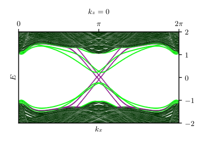
We show in Fig. 4 the band structure of the system (panel a) at , as well as the real-space probability distribution of the in-gap modes at the Dirac cone momenta (panel b). Each surface of the WTI slab still shows gapless modes, as expected, which are colored in red and blue, as in Fig. 1. In addition, however, there now appear gapless states localized at the stacking fault plane, colored green, which are 2D gapless states embedded in the middle of the gapped, 3D WTI bulk.
The analogy to the 1D SSH model proves to be correct in predicting the gapless nature of the stacking fault in the single-spacer WTI. This simple heuristic argument, however, fails to accurately describe the robustness of the stacking fault modes. In the SSH chain, while the absence of dimerization does produce a gapless phase, the latter is a fine-tuned point in the parameter space, one at which a topological phase transition takes place. In contrast, as we show in the following, the 2D gapless phase of the planar defect is robust against perturbations, being protected by mirror symmetry.
Consider a WTI slab in the presence of a stacking fault, infinite along but having a finite width along , as shown in Fig. 2(a). The unit cell of the full system (shown in red) is composed of four building blocks: the topological layers on the left and right of the defect, which we label and , and the trivial layers on the left and right, labeled and . We write the full slab Hamiltonian as , with a column vector formed by all annihilation operators of the system and the Hamiltonian matrix. In the grading of the four blocks mentioned above this matrix takes the form
| (5) |

Here we have considered that the stacking fault is positioned in the middle of the slab, such that and are matrices of equal size, with thicker slabs leading to larger matrices. The term, is a Hamiltonian block containing all of the nearest-neighbor hopping terms across the stacking fault, the ones which serve to glue the two halves of the system back together. , , as well as depend on the momentum but are independent of , since they only encode the on-site and hopping terms within the trivial and topological layers, as well as the in-plane hoppings between them.
All of the hoppings along the stacking direction, , are included in the term appearing in the off-diagonal blocks of Eq. (5) and in the diagonal term . Part of the off-diagonal term includes the vertical hoppings connecting the trivial and topological layers within the same unit cell, and is thus momentum independent, whereas the second part contains the hoppings connecting layers across the unit cell boundary, hence the factor . These vertical hoppings are given by the inter-layer coupling Hamiltonian of Eq. (3), meaning that , with an identity matrix of the same size as the number of sites in and . It follows that , which explains the relative minus sign. The diagonal term contains the next nearest neighbor hoppings connecting the TI (and the trivial) layers to each other. This term obeys .
Using the form of Eq. (5) and the properties of and , it becomes apparent that the slab Hamiltonian obeys a mirror symmetry. The mirror plane is perpendicular to the stacking direction, thus mapping , such that
| (6) |
The mirror operator, written in the grading of Eq. (5), is a block-diagonal matrix composed of four blocks: . Note that is a spinful mirror symmetry which commutes with the time-reversal symmetry operator, , where is an identity matrix acting on all of the sites of the slab’s unit cell and is complex conjugation.
The mirror symmetry protects the Dirac cones at but not the ones at . On the mirror-invariant plane of the Brillouin zone, , the trivial and topological layers are effectively decoupled in the vertical direction. The states of and are associated to a mirror eigenvalue , whereas those of , are orthogonal to them, having a mirror eigenvalue (as shown in Fig. 1). Mirror symmetry thus prevents the topological modes of the QSHE layers on either side of the stacking fault from coupling to each other, guaranteeing the formation of gapless phase at the planar defect. The latter forms an embedded, 2D topological semimetal protected by mirror symmetry. In contrast, at , the QSHE modes on the left and right of the stacking fault have the same mirror eigenvalues, and are therefore not protected.
IV.2 Double spacer
We now consider a stacking fault in the two-spacer WTI. In this case we shift half of the system in the direction by either or of the unit cell. When the system has an infinite number of layers, these two scenarios differ only in the choice of the unit cell. In both cases, the corresponding infinite SSH chain is in a insulating phase and the spectrum of the system should be gapped.
We have created, as before, two identical copies of the system shifted with respect to each other in the by of the unit cell. In this way every TI layer on one side of the stacking fault has a trivial layer on the opposite side. The two sides are glued together, as before, using the nearest-neighbor hopping .
In this case, the helical modes at the stacking fault develop a gap at both the Dirac points at , and the system has no mirror symmetry. We obtain an embedded SSH-like system with at the defect, as we expected.
To distinguish between the topological and trivial phase of the SSH model, we study a system with a finite number of layers to detect the boundary states at the beginning and at the end of the stacking fault. In a system with a finite number of layers we will have more bands near the the Fermi level . In order to distinguish the bands associated with the topological states at the boundaries of the stacking fault, is convenient to make the gap larger. We achieve this by replacing the Hamiltonian in Eq. (4) with:
| (7) |
where for sites that belong to the A or B sublattice respectively. The new term, , couples equal-spin components of the surface states. Components with the same spin of helical modes at opposite sides of the defect will have opposite velocity, so this new term will produce a bigger gap at the stacking fault, see Fig. 5.
IV.3 Topological edge states at the stacking fault

In order to check the presence of topological states at the defect in the tight-binding model, we build a system with a finite height, . To better visualize the stacking fault modes, we add periodic boundary conditions in the direction, such that the system contains two stacking faults. In this way we eliminate the surface modes and obtain only the spectrum of the two defects.
The SSH chain associated with the WTI with two trivial spacers will be in the trivial () or in the topological () phase depending on the boundary conditions at the stacking fault. If the defect begins and ends with a couple of dimerized TI layers, we do not find any gapless states (see Fig. 6), similar to the infinite case.

For a system with two weakly-coupled TI layers at the boundary of the defect, the corresponding SSH chain is in the topological phase. In this case, we find topological gapless bands located at the boundaries of the two stacking faults, see Fig. 6. We confirm their location by plotting the real-space probability distribution, , as a function of the position in the unit cell in Fig. 7.
V Conclusions
In order to explore the effect of stacking faults in weak topological insulators like and , we have used a tight binding model composed of stacked honeycomb QSHE layers. We have then used a heuristic argument to draw an analogy between the physics of the topological states at the defect and an SSH chain.
The stacking fault in a WTI with one trivial spacer per unit cell behaves like an SSH at the gap closing point. Thus, it forms an embedded topological semimetal, which we have shown to be protected by mirror symmetry. In contrast, a WTI with two insulating spacers per unit cell behaves like an SSH chain in the topological or trivial phase, depending whether or not it has weakly-coupled TI layers at the edges of the stacking fault. In the latter case, an embedded topological insulator is formed: the stacking fault hosts 1D gapless modes at its boundaries.
This means that it is in principle possible to obtain embedded topological insulators or semimetals inside the bulk of a WTI in the presence of a stacking fault. In this case the defect is not destroying the topological properties of the system, but is a source of new, robust states.
Our toy model is only qualitative in nature. A quantitative prediction of the real properties of stacking faults in and would require more accurate numerical methods, such as density functional theory. Nevertheless, the analogy to the SSH model may still be used to guide this endeavor. For instance, while stacking faults obtained by a fractional translation have not been reported to date in these materials, it has been shown that Bi2TeI forms inverted twin domains Zeugner et al. 2017; Zeugner et al. 2018. Since its unit cell is composed of one QSHE layer and two spacers, we conjecture that these stacking faults will host protected gapless modes at their boundaries whenever they are terminated by weakly-coupled TI layers.
VI Acknowledgments
We thank Ulrike Nitzsche for technical assistance. We acknowledge financial support from the DFG through the Würzburg-Dresden Cluster of Excellence on Complexity and Topology in Quantum Matter – ct.qmat (EXC 2147, project-id 39085490).
References
- Klitzing et al. (1980) K. v. Klitzing, G. Dorda, and M. Pepper, New method for high-accuracy determination of the fine-structure constant based on quantized Hall resistance, Phys. Rev. Lett. 45, 494 (1980).
- Thouless et al. (1982) D. J. Thouless, M. Kohmoto, M. P. Nightingale, and M. den Nijs, Quantized Hall conductance in a two-dimensional periodic potential, Phys. Rev. Lett. 49, 405 (1982).
- Kane and Mele (2005a) C. L. Kane and E. J. Mele, Quantum spin Hall effect in graphene, Phys. Rev. Lett. 95, 226801 (2005a).
- Kane and Mele (2005b) C. L. Kane and E. J. Mele, topological order and the quantum spin Hall effect, Phys. Rev. Lett. 95, 146802 (2005b).
- Bernevig et al. (2006) B. A. Bernevig, T. L. Hughes, and S.-C. Zhang, Quantum spin Hall effect and topological phase transition in HgTe quantum wells, Science 314, 1757 (2006).
- König et al. (2007) M. König, S. Wiedmann, C. Brüne, A. Roth, H. Buhmann, L. W. Molenkamp, X.-L. Qi, and S.-C. Zhang, Quantum spin Hall insulator state in HgTe quantum wells, Science 318, 766 (2007).
- Kitaev et al. (2009) A. Kitaev, V. Lebedev, and M. Feigel’man, Periodic table for topological insulators and superconductors, AIP Conference Proceedings 1134, 22 (2009).
- Ryu et al. (2010) S. Ryu, A. P. Schnyder, A. Furusaki, and A. W. W. Ludwig, Topological insulators and superconductors: Tenfold way and dimensional hierarchy, New J. Phys. 12, 065010 (2010).
- Hasan and Kane (2010) M. Z. Hasan and C. L. Kane, Colloquium: Topological insulators, Rev. Mod. Phys. 82, 3045 (2010).
- Fu et al. (2007) L. Fu, C. L. Kane, and E. J. Mele, Topological insulators in three dimensions, Phys. Rev. Lett. 98, 106803 (2007).
- Moore and Balents (2007) J. E. Moore and L. Balents, Topological invariants of time-reversal-invariant band structures, Phys. Rev. B 75, 121306 (2007).
- Roy (2009) R. Roy, Topological phases and the quantum spin Hall effect in three dimensions, Phys. Rev. B 79, 195322 (2009).
- Benalcazar et al. (2017) W. A. Benalcazar, B. A. Bernevig, and T. L. Hughes, Quantized electric multipole insulators, Science 357, 61 (2017).
- Schindler et al. (2018) F. Schindler, A. M. Cook, M. G. Vergniory, Z. Wang, S. S. P. Parkin, B. A. Bernevig, and T. Neupert, Higher-order topological insulators, Sci. Adv. 4, aat0346 (2018).
- Fu (2011) L. Fu, Topological crystalline insulators, Phys. Rev. Lett. 106, 106802 (2011).
- Hsieh et al. (2012) T. H. Hsieh, H. Lin, J. Liu, W. Duan, A. Bansil, and L. Fu, Topological crystalline insulators in the SnTe material class, Nat. Commun. 3, 982 (2012).
- Ando and Fu (2015) Y. Ando and L. Fu, Topological crystalline insulators and topological superconductors: From concepts to materials, Annu. Rev. Condens. Matter. Phys. 6, 361 (2015).
- Zhang et al. (2018) Z. Zhang, R.-W. Zhang, X. Li, K. Koepernik, Y. Yao, and H. Zhang, High-throughput screening and automated processing toward novel topological insulators, Phys. Chem. Lett 9, 6224 (2018).
- Fulga et al. (2014) I. C. Fulga, B. van Heck, J. M. Edge, and A. R. Akhmerov, Statistical topological insulators, Phys. Rev. B 89, 155424 (2014).
- Teo and Kane (2010) J. C. Y. Teo and C. L. Kane, Topological defects and gapless modes in insulators and superconductors, Phys. Rev. B 82, 115120 (2010).
- Ran et al. (2009) Y. Ran, Y. Zhang, and A. Vishwanath, One-dimensional topologically protected modes in topological insulators with lattice dislocations, Nat. Phys. 5, 298 (2009).
- Teo and Hughes (2017) J. C. Teo and T. L. Hughes, Topological defects in symmetry-protected topological phases, Annu. Rev. Condens. Matter. Phys. 8, 211 (2017).
- Juričić et al. (2012) V. Juričić, A. Mesaros, R.-J. Slager, and J. Zaanen, Universal probes of two-dimensional topological insulators: Dislocation and -flux, Phys. Rev. Lett. 108, 106403 (2012).
- Hughes et al. (2014) T. L. Hughes, H. Yao, and X.-L. Qi, Majorana zero modes in dislocations of Sr2RuO4, Phys. Rev. B 90, 235123 (2014).
- Teo and Hughes (2013) J. C. Y. Teo and T. L. Hughes, Existence of Majorana-fermion bound states on disclinations and the classification of topological crystalline superconductors in two dimensions, Phys. Rev. Lett. 111, 047006 (2013).
- Benalcazar et al. (2014) W. A. Benalcazar, J. C. Y. Teo, and T. L. Hughes, Classification of two-dimensional topological crystalline superconductors and Majorana bound states at disclinations, Phys. Rev. B 89, 224503 (2014).
- Ringel et al. (2012) Z. Ringel, Y. E. Kraus, and A. Stern, Strong side of weak topological insulators, Phys. Rev. B 86, 045102 (2012).
- Tretiakov et al. (2010) O. A. Tretiakov, A. Abanov, S. Murakami, and J. Sinova, Large thermoelectric figure of merit for three-dimensional topological Anderson insulators via line dislocation engineering, Appl. Phys. Lett. 97, 073108 (2010).
- Sbierski et al. (2016) B. Sbierski, M. Schneider, and P. W. Brouwer, Weak side of strong topological insulators, Phys. Rev. B 93, 161105 (2016).
- Hamasaki et al. (2017) H. Hamasaki, Y. Tokumoto, and K. Edagawa, Dislocation conduction in Bi-Sb topological insulators, Appl. Phys. Lett. 110, 092105 (2017).
- Shiozaki and Sato (2014) K. Shiozaki and M. Sato, Topology of crystalline insulators and superconductors, Phys. Rev. B 90, 165114 (2014).
- Slager et al. (2014) R.-J. Slager, A. Mesaros, V. Juričić, and J. Zaanen, Interplay between electronic topology and crystal symmetry: Dislocation-line modes in topological band insulators, Phys. Rev. B 90, 241403 (2014).
- Queiroz et al. (2019) R. Queiroz, I. C. Fulga, N. Avraham, H. Beidenkopf, and J. Cano, Partial lattice defects in higher-order topological insulators, Phys. Rev. Lett. 123, 266802 (2019).
- Roy and Juričić (2021) B. Roy and V. Juričić, Dislocation as a bulk probe of higher-order topological insulators, Phys. Rev. Research 3, 033107 (2021).
- Yamada et al. (2022) S. S. Yamada, T. Li, M. Lin, C. W. Peterson, T. L. Hughes, and G. Bahl, Bound states at partial dislocation defects in multipole higher-order topological insulators, Nat. Commun. 13, 2035 (2022).
- Tuegel et al. (2019) T. I. Tuegel, V. Chua, and T. L. Hughes, Embedded topological insulators, Phys. Rev. B 100, 115126 (2019).
- Velury and Hughes (2021) S. Velury and T. L. Hughes, Embedded topological semimetals, arXiv.2108.07813 (2021).
- Rusinov et al. (2016) I. P. Rusinov, T. V. Menshchikova, A. Isaeva, S. V. Eremeev, Y. M. Koroteev, M. G. Vergniory, P. M. Echenique, and E. V. Chulkov, Mirror-symmetry protected non-TRIM surface state in the weak topological insulator Bi2TeI, Sci. Rep. 6, 20734 (2016).
- Rasche et al. (2013) B. Rasche, A. Isaeva, M. Ruck, S. Borisenko, V. Zabolotnyy, B. Büchner, K. Koepernik, C. Ortix, M. Richter, and J. van den Brink, Stacked topological insulator built from Bismuth-based graphene sheet analogues, Nat. Mater. 12, 422 (2013).
- Rasche et al. (2016) B. Rasche, A. Isaeva, M. Ruck, K. Koepernik, M. Richter, and J. van den Brink, Correlation between topological band character and chemical bonding in a Bi14Rh3I9-based family of insulators, Sci. Rep. 6, 20645 (2016).
- Murakami (2006) S. Murakami, Quantum spin Hall effect and enhanced magnetic response by spin-orbit coupling, Phys. Rev. Lett. 97, 236805 (2006).
- Avraham et al. (2020) N. Avraham, A. K. Nayak, A. Steinbok, A. Norris, H. Fu, Y. Sun, Y. Qi, L. Pan, A. Isaeva, A. Zeugner, C. Felser, B. Yan, and H. Beidenkopf, Visualizing coexisting surface states in the weak and crystalline topological insulator bi2tei, Nat. Mater. 19, 610 (2020).
- Zeugner et al. (2017) A. Zeugner, M. Kaiser, P. Schmidt, T. V. Menshchikova, I. P. Rusinov, A. V. Markelov, W. Van den Broek, E. V. Chulkov, T. Doert, M. Ruck, and A. Isaeva, Modular design with 2d topological-insulator building blocks: Optimized synthesis and crystal growth and crystal and electronic structures of BixTeI (), Chemistry of Materials 29, 1321 (2017).
- Zeugner et al. (2018) A. Zeugner, J. Teichert, M. Kaiser, T. V. Menshchikova, I. P. Rusinov, A. V. Markelov, E. V. Chulkov, T. Doert, M. Ruck, and A. Isaeva, Synthesis, crystal and topological electronic structures of new bismuth tellurohalides Bi2TeBr and Bi3TeBr, Chemistry of Materials 30, 5272 (2018).
- Goerbig (2011) M. O. Goerbig, Electronic properties of graphene in a strong magnetic field, Rev. Mod. Phys. 83, 1193 (2011).
- Das et al. (2019) S. K. Das, B. Yan, J. van den Brink, and I. C. Fulga, Topological crystalline insulators from stacked graphene layers, Phys. Rev. B 99, 165418 (2019).
- Groth et al. (2014) C. W. Groth, M. Wimmer, A. R. Akhmerov, and X. Waintal, Kwant: a software package for quantum transport, New J. Phys. 16, 063065 (2014).
- Naselli et al. (2022) G. Naselli, V. Könye, S. K. Das, G. G. N. Angilella, A. Isaeva, J. van den Brink, and C. Fulga, Nontrivial gapless electronic states at the stacking faults of weak topological insulators, Zenodo: https://doi.org/10.5281/zenodo.6638289 (2022).
- Su et al. (1979) W. P. Su, J. R. Schrieffer, and A. J. Heeger, Solitons in polyacetylene, Phys. Rev. Lett. 42, 1698 (1979).