Role of optical rectification in photon-assisted tunneling current
Abstract
We study the optical rectification in a metallic tunnel junction. We consider a planar junction in a Kretschmann configuration and measure the photon-assisted tunneling under infrared illumination at . To address the microscopic mechanism at the origin of the optical rectification, we compare the photon assisted current and the current-voltage characteristics of the junction measured on a voltage range much greater than . The experimental results do not agree with the Tucker theory based on the exchange of energy quanta between electrons and photons and describing the dc current induced by photon-assisted processes in terms of a linear combination of the shifted characteristics and . We show instead that the illumination power mainly goes into heating and that the rectification results mainly from the non-linearity of the tunnel junction at optical frequency.
I Introduction
Recent years have seen tremendous progress in nanophotonics with the realization of optical antennas which can receive Muhlschlegel2005; Bharadwaj2009 and emit radiation at optical frequencies Qian_2018; Zhang_2019; Qian_2021. In terms of detectors, nanoantennas allow an efficient transfer of radiation into surface plasmons and they close the gap between the characteristic lengths of optics (micrometer scale) and electronic devices (nanometer scale). Thus, if coupled with a non-linear element, they can be used for optical rectification. One thus refers to rectenna: a nanoantenna converts the optical radiation into an ac voltage which is in turn converted to a dc current through a rectifier (diode). However, optical rectification in conductors raises central questions. (i) Is it possible to define a voltage at optical frequencies as used in the microwave domain? A microwave excitation of frequency at low temperature () actually induces discontinuities in the derivative of distribution function at energies with integer Kozhevnikov_2000. (ii) Is it possible to observe this kind of step like distribution function at optical energies? While they are linear elements at low voltage bias (i.e ), Metal-Insulator-Metal (MIM) junction becomes strongly non-linear at optical frequencies () and are promising rectifiers. The goal of this article is to focus on MIM junctions as an optical rectifier and to address the underlying microscopic mechanism.
The photon-assisted tunnelling (PAT) has been investigated in experiments using microwave radiation, where the illumination is simply described by an ac bias voltage, , across the conductor Tucker_1985; Kouwenhoven_1994; Gabelli_2008. In this regime, the PAT is well described in the quantum limit, , by the approach of Tien and Gordon Tien_1963 where this time dependent potential, creates a non-equilibrium distribution function in the reservoir absorbing the radiation and corresponding to energy quanta exchange between electrons and microwave photons. It is tempting to describe the optical rectification within the same theory by describing the illumination by an optical voltage . In the following, we consider the excess current due to illumination: where is the current in the absence of incident light and the current under illumination. As demonstrated below , the time-averaged photon-assisted tunneling current calculated from the distribution functions predicted by Tien and Gordon, is then given at the first non-vanishing order in , by the Tucker formula (TF):
| (1) |
where , is the Planck constant and the elementary charge. Below we will address the full quantum regime . This is technically demanding as it requires to be able to polarize a MIM junction with a voltage bias without deteriorating the device. We are not aware of previous work in this regime. To do so, we have chosen to perform the experiment on a robust Al/AlOx/Al tunnel junction at low temperature to prevent junction aging effects as experimentally verified in our previous works Fevrier_2018. We use infrared radiation corresponding to . We found that PAT in MIM junctions can not be explained by the theory of quantum detection as expected by eq. (1). Knowing that the Fermi-liquid theory Pine_Nozieres_1966 gives lifetime of an excited electron of the order of , the lifetime of quasiparticles excited by optical photons is more than eight order of magnitude shorter than the ones excited by microwaves. For electrons with energy above the Fermi energy, we estimate . This lifetime can only be accessed by time-resolved photoemission spectroscopy Fann_1992; Campillo_1999. As a consequence, the tunnel spectroscopy under continuous wave illumination can hardly reveal non-thermal distributions Sivan2019. As a result, our data are well described by thermal distribution functions characterized by a temperature in each electrode and highlight a tunneling Seebeck effect.
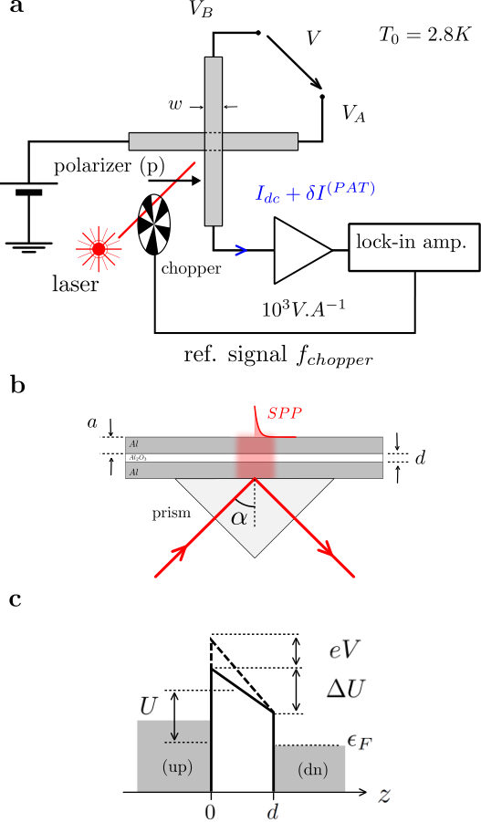
The article is organized as follows. The sample and the experimental setup are described in section II. To increase the amount of radiation absorbed by the MIM, we convert the far field radiation into a local electromagnetic mode by means of a surface plasmon polariton (SPP) resonance. We probe the SPP resonance by PAT in section III. We then measure the right and left hand sides of eq. (1) independently. We discuss the validity of eq. (1) in the optical regime by using the Simmons tunnel barrier model in section IV Simmons_1964. In order to probe in more detail the interplay between illumination and the electron distribution in metallic thin films, we compare our measurement with the two possible senari: the hot carrier distribution functions characterized by a step like function at optical energies and the equilibrium distribution function at different temperatures.
II Sample fabrication and experimental setup
The sample is a metallic cross-junction deposited on a standard microscope cover glass. The aluminum electrodes thickness is and the tunneling barrier is obtained by Al oxidation performed in a glow discharge. The characteristics fit Simmons_1964 enables to determine the barrier characteristics depicted in Fig. 1 c: thickness , barrier height and barrier asymmetry . A right angle prism is glued with a UV-curing glue on the rear of the glass to allow the SPP excitation by the incoming optical radiation in a Kretschmann configuration Kretschmann_1972 (see Fig. 1 b). The experimental setup is shown in Fig. 1a. The junction is mounted on a rotating stage in a cryogen-free refrigerator at enabling the excitation of the SPP resonance (SPR). The characteristics of the junction is measured using a standard four-point probe method simultaneously with the photon assisted current. The current generated due to the radiation is given by a lock-in amplifier referenced to the optical chopper at frequency ranging from to . The SPP mode is transverse magnetic. It is excited by a p-polarized light at the resonance angle with the refractive index of the cover glass (see Appendix A). The p-polarization is set by adjusting a linear polarizer in the fridge at room temperature and small bias voltage before cooling. Figure 2 clearly shows the effect of the field enhancement due to surface plasmon resonance on the PAT Berthold_1985 at . In the following, we will consider PAT current induced by this resonance. It corresponds to an enhancement of the electromagnetic field in the tunnel junction by a factor 3.
III Photon-assisted tunneling at infrared frequencies
The responsivity of a rectifier is given by the ratio between the photon-assisted current and the optical absorbed power . Let’s assume that optical excitation induces an ac signal of amplitude at frequency . The related ac current is given by where stands for the conductance at frequency . In the classical limit of small ac excitation ( and ), the conductance is associated to the adiabatic response of the characteristics and the time-averaged current is proportional to its second derivative . Surprisingly this classical limit seems to account for the experimental results of Ward et al Ward_2010 out of its regime of validity . With the hypothesis that the optical absorbed power is equal to the electrical one , the responsivity can be rewritten by as for a classical diode. Following the same assumption and using the Tucker’s description of the electronic transport in a metallic tunnel junction at finite frequencies, the conductance is given by and the responsivity in the quantum regime reads Grover2013:
| (2) |
Figure 3 shows the experimental responsivity measured as a function of the bias voltage for different laser powers at SPR. The absorbed power at SPR is proportional to the laser power: (see Fig. 2a and Appendix A). As shown in eq. (2), the responsivity does not depend on the illumination power. The conversion efficiency of the metallic tunnel junction is independent of the incident optical power and acts as linear photon detector for the investigated power range (). We estimate the maximal experimental responsivity at SPR: . By using the measured characteristics between and (see inset Fig. 3), we estimate the theoretical responsivity between and . We see in Fig. 3 that does not have the same voltage dependence (black dashed line) and is more than seven orders of magnitude smaller than the theoretical value given by eq. (2). This requires some more investigation which we do here below.
IV Validity of the Tucker formula
Equation (2) is convenient because it directly gives the photon responsivity of the junction from its electrical characteristics . However, this description is based on two strong hypothesis: (i) the photon-assisted processes can be described by an optical voltage biasing of the junction and (ii) the absorbed power is given by the electric resistance of the junction evaluated at optical frequency. Let us briefly show how to establish eq. (1). The effect of voltage bias due to the dc bias and the laser illumination is to shift adiabatically the Fermi sea of the upper reservoir sustaining the surface plasmon while the lower reservoir is grounded. The resulting time averaged out-of-equilibrium distribution function in the upper reservoir is then given by the Tien-Gordon formula Tien_1963; Blanter_2000:
| (3) |
where is the Bessel’s function of the first kind and is the Fermi–Dirac distribution with the Fermi energy and the electron temperature. Using a Landauer-Büttiker scattering approach, we express the time-average PAT current as:
| (4) |
Using and assuming that transmission is voltage independent , one deduces:
| (5) |
If one only considers the one photon apsorption/emission processes at energies (), eq. (5) corresponds to eq. (1) by retaining the lowest order terms in . Note that eq. (4) is explicitly not gauge invariant Aguado2003. This hypothesis is valid in the microwave regime where the alternative electric field is well described by a voltage drop across the junction (one electrode is effectively grounded). However, it remains a strong assumption in optics where the lower electrode is not grounded at optical frequencies and the associated vector potential does play a role. In what follows, we focus on the experimental verification of eq. (1). To do so, we probe in a range of and the characteristics in a range of . Figure 4 shows the PAT current measured by optically chopping of the laser beam at . The data are compared to the TF photon assisted tunneling current given by eq. (1). Note that this quantity is directly measured. The only free parameter is the optical voltage which is adjusted with the slope of at zero dc bias. We then deduce an optical voltage . This value is overestimated by more than four orders of magnitude in view of the laser power (according to Appendix A corresponds to ). More importantly equation (1) does not account for the experimental data neither qualitatively or quantitatively. As mentioned above, this equation assumes that tunnel transmission is voltage independent: . This is not the case at bias voltage of the order of the tunnel barrier height. Instead, the transmission is calculated by modelling the junction by a trapezoidal barrier Simmons_1964 (see inset Fig. 3 and Appendix B). A numerical evaluation of eq. (4) gives a smaller but still unrealistic optical voltage . In conclusion, the fitting parameters using TF are not physical. Our experiment confirms that the description of the photon-assisted tunneling as an optical rectification cannot explain the photon-assisted processes in a tunnel junction. A more realistic description is to consider the Boltzmann equation (BE) describing electron dynamics in metallic systems Voisin_2000.
V Hot-carrier vs thermal distribution
The PAT current of eq. (4) can be re-written in terms of the deviation of the electron distribution from the equilibrium:
| (6) |
where states for the deviation of the electron distribution from the equilibrium distribution at base temperature . This steady-state non-equilibrium electron distribution function under continuous wave illumination is given by the master equation:
| (7) |
where is the electron distribution function, the first term stands for electron-phonon energy transfer between electrons and lattice, the second stands for electron-electron thermalization (characterized by an electron collision time of the order of few 100 fs) while the third term describes the excitation due to photon absorption in the contacts. The first two terms will mainly lead to an equilibrium distribution characterized by an effective temperature. The excitation term could however lead to the existence of a small fraction of hot electron. we evaluate below what would be the effect of a hot electron distribution on the PAT. It can be evaluated by considering a detailed balanced equation and the Fermi golden rule (Appendix C):
| (8) |
where is a constant proportional to the energy absorbed by electrons. In the relaxation time approximation for the electron-electron thermalization , we deduce the time-average PAT current of eq. (4) due to hot-carrier contribution by considering the deviation of the electron distribution . is a constant proportional to the energy absorbed in the upper/lower electrode. It is convenient to characterize this amount of energy by expressing it in terms of equivalent temperature of excitation . To do so, we consider a Fermi-Dirac distribution at containing the same energy as the non-equilibrium distribution function:
| (9) |
where is the density of states of the free electron gas. Figure 5 shows the photon-assisted current as a function of dc current flowing through the junction biased between and . It is mainly proportional to the current. Dashed blue line in figure 5 corresponds to the theoretical prediction given by eqs. (8,6). We clearly see that the proportionality cannot be explained by a hot-carrier distribution function. We fit by adjusting the absorption coefficients and with an optimization software. Note that is in agreement with the fact that upper electrode experiences the field enhancement of the surface plasmon. They corresponds to equivalent temperatures of excitation of and respectively. Even if this term leads to a Tien-Gordon-like distribution given by eq. (3), the hot carrier distribution remains extremely small because of electron heating and heat leakage to the lattice as studied by Dubi and Sivan Sivan2019; Bouhelier_2021. Moreover, the equivalent temperature of excitation is smaller than and we see in the following that this temperature remains smaller than the temperature induced by the power absorption in the lead. It follows that the photon absorption mainly induces heating rather than generating hot carriers. In the following, we analyze the PAT current as resulting from two different thermal distributions in the contacts and can be refereed as a the tunneling Seebeck effect Stovneng_1990. However, unlike the Seebeck effect which depends on the metallic density of states of the electrode materials, the tunneling Seebeck effect depends on the energy dependence of the tunneling transmission and so that on the non linearity of the characteristic Smith_1980. The PAT current is then described by eq. (6) with the deviation of the electron distribution . is the temperature of upper/lower electrode.
Figure 5 shows the proportionality between the photon assisted current and the current. This proportionality is explained by a differential heating between the upper and lower electrodes. Our data are in good agreement with the heating description (red dashed line in Fig. 5). We have checked that the PAT measured across the junction is one order of magnitude greater than the photon assisted current in each electrode. The cross geometry of the tunnel junction allows us to measure the photon-assisted current in the upper/lower electrode by using a current polarization of the upper/lower electrode. The power supply is connected on the contact (resp. ) to measure the upper (resp. lower) electrode (see Fig. 2) while the current amplifier is connected to the opposite side of the electrode. Inset of figure 5 shows the photo-assisted current measured in the two electrodes independently. This photon assisted current is attributed to a variation of the aluminum conductivity. The Drude conductivity is indeed proportional to the relaxation time which depend on the temperature so that a laser induced temperature modulation will induce a conductance modulation. The energy and voltage dependent transmission of the barrier is deduced from the fit of the curve. The fit of the curve gives and . The temperature rise can be associated with the optical power absorbed by the electrodes. The junction in the Kretschmann configuration forms a well defined plasmonic multilayer stack and the absorbed power at the resonance angle are evaluated to and respectively (Appendix A). We neglected the power leakage due to thermal conduction of the contacts and identify the absorbed power and the power dissipated to the lattice of volume . The temperature rise in the electrodes is thus estimated to where the electron-phonon coupling constant in aluminum Meschke_2004 is . It gives and . Note that the estimated temperature rise is slightly underestimated. It can be attributed to the value of the dielectric constant that we have considered Rakic_1995 knowing we consider here an unusual ultra-thin aluminum film. The photon-assisted tunneling is strictly speaking a thermo-assisted tunneling. Our measurement could also be sensitive to the variation of the electrode conductance due to their temperature modulation. Thanks to the cross-geometry of the junction, we have checked that this effect is negligible compare to the PAT measured on the junction. The inset of Fig. 5 shows that the photon-induced current in the electrodes is lower by more than one order of magnitude compared to the PAT current. The modulation of the light power by the chopper (laser on/off) induces a modulation of the resistance of the electrodes: . When the electrode is voltage bias, this translates in a photon-induced current given by . The inset of Fig. 5 shows that the photon induced current in the electrodes corresponds to a relative increase of their resistance () Herzog_2014: and . Using the Sommerfeld expansion in the electrical conductivity and assuming a linear dependence of the relaxation time, we expect a quadratic temperature dependence of the conductivity so that (see Appendix D). We then deduce a ratio which is consistent with the measured ratio .
VI Conclusion
Optical rectification in metallic tunnel junctions produces dc photocurrent assuming that illumination acts as an ac voltage at optical frequencies across the nonlinear tunnelling conduction. The photon-assisted transport theory in tunnel junctions states that the dc photocurrent is a well known function of the characteristics on a voltage range of the photon voltage . This theoretical prediction is based on the creation of a non-thermal hot carrier distribution function in the metals under optical illumination. We have shown experimentally that this is incorrect in a planar tunnel junction. By comparing the photocurrent generated in a planar junction in the Kretschmann configuration and the measured characteristics, we have demonstrated that the photocurrent can be described by heating and thermal distribution functions instead. While we have only considered a planar tunnel junction without nanoantenna, the question of the generation of hot electrons in metallic nanostructures for optical rectification or optical detection still raises theoretical questions. As pointed out by Iñarrea et al. in the case of THz detectors in double barrier systems Inarrea_1994, it is crucial to calculate the transmission coefficient by considering the coupling term where is the vector potential of the electromagnetic field and the electronic momentum operator. Note that the coupling between electrons and the electromagnetic field no longer takes place in a single region of the structure but interacts with the barrier. In conclusion, the planar tunnel junction is not a good candidate to highlight the hot carrier distribution in illuminated metallic thin films. The metallic density of states is indeed to smooth and it does not allow the realization of the necessary energy filter as it is in a molecular junction Dubi_2022.
Appendix A: Plasmonic multilayer stack
We consider an MIM stack on top of a righ angle prism (see Fig. 6). The thickness of the metallic films is and that of dielectric barrier is . The dielectric constants of metal and barrier are respectivelly and at Rakic_1995; Dodge_1986.
We consider the Fresnel coefficients for a TM-polarised light (p polarized). For a single interface from (1) to (2) between two dielectric materials characterized by the dielectric constant and respectively, the reflexion and transmission Fresnel coefficients read:
| (10) |
By using the Fresnel’s coefficients on the interfaces at , the amplitude of the incoming and outgoing magnetic field are connected by a transfer matrix:
| (11) |

The p-polarized magnetic fields in the different regions are defined by:
with,
The color plot Fig. 7 shows the surface plasmon resonance (SPR) at the angle . This angle corresponds approximatively to the critical angle with the refractive index of the cover glass. is the incident angle enabling the coupling between the light in the cover glass and the surface plasmon propagating on the interface upper electrode/vacuum. Figure 7 shows the amplitude of the normalized magnetic field inside the junction. The measured SPR (see Fig. 2) is broader than the simulated one probably due to the roughness of our ultra-thin film deposition. At angle , the field enhancement occurs on the upper electrode. The electric field is deduced from the magnetic field:
| (14) |
The optical voltage between the two upper and lower electrodes is then given by:
| (15) |
and it is maximum around the SPR: (see Fig. 9 a). The absorbed power in the different regions of the junction is given by:
| (16) |
Figure 9b shows that the upper electrode absorbs more power than the lower one at SPR: whereas . Note that the power dissipated in the barrier is negligible and that it is reasonable to assume that the barrier transmission is not affected by any thermal effects.
Appendix B: Tunnel transmission

In order to calculate the different quantities related to the photon-assisted tunneling current in the far from equilibrium regime, we model the tunnel barrier by a trapezoidal barrier characterized by a thickness , a mean height and an asymmetry (see Fig. 11). This allowed us to obtain an analytical expression of the tunnel transmission . This analytical expression is essential to perform numerical optimization on the characteristics (see Fig. 3) and the photon assisted current (see Fig. 5 and eq. (6)).
We are considering the Simmons’ model where an effective potential includes the potential barrier and the biasing energy , . The 3D transmission can be expressed as a function of the Wentzel–Kramers–Brillouin (WKB) transmission through the 1D effective potential Simmons_1964; Fevrier_2018:
| (17) |
We can distinguish three cases: (i) the energy is smaller that the barrier and the electrons see a trapezoidale barrier () (ii) the electrons see a triangular barrier ( and (iii) the electrons go over the barrier (). These cases depend on the values of and :
- •
if then
- •
if then
- •
if then
- •
if then
Appendix C: Non-equilibrium distribution function
The interplay between photons and electrons in the metallic contact may lead to ”hot” electron distribution junction or heating. For a moderate increase of temperature, the heating affects a large number of quasiparticles around the Fermi sea whereas the photon-assisted processes brings a small amount of quasiparticles at high energy corresponding to the photon energy (see Fig. 12). The excitation of the conduction electrons is done by the absorption of photons of energy . Assuming that the processes of excitation involve only intraband transitions, electrons of energy reach energy . The change in occupancy number is given by the difference between the number of electrons that access the energy and the number of electrons that leave it:
where is the density of states of the free electron gas, is a constant proportional to the energy transfered to the electron gas and the equilibrium Fermi-Dirac distribution. The change in the occupancy number is given by . The excitation term in eq. (8) is then directly deduced.
The normalized difference between the energy contained in the non-equilibrium distribution function characterized by absorbed power coefficient and the equilibrium function at temperature is given by:
The equivalent temperature of excitation corresponds to . Figure 13 gives the values of for the upper electrode () and the lower one ().
Appendix D: Temperature dependence of the conductivity
Using the free electron gas model to describe the electron transport in the metallic electrodes, the Boltzmann equation and the relaxation time approximation give the electrical conductivity:
| (20) |
where is the density of electrons, the effective masse of electrons, the elementary charge and the mean value of the relaxation time . By considering the density of states in 3D, the mean value is given by:
| (21) |
In the first order approximation near the Fermi energy, the relaxation time can be written as . The Sommerfeld expansion of gives:
| (22) |
and the relative increase of the resistance is thus:
| (23) |
Assuming that the energy dependence of the relaxation time is the same in both aluminum electrodes, the ratio gives access to the ratio .
Acknowledgements. We acknowledge fruitful discussions with Marc Bescond. We also thank Sylvie Gautier for the help in sample fabrication and Gilles Guillier for the cryognetic rotation realization. This work has been supported by Region Ile-de-France in the framework of DIM SIRTEQ.
References
- (1) P. Mühlschlegel, H. J. Eisler, O. J.F. Martin, B. Hecht and D. W. Pohl , Science 308 1607 (2005)
- (2) P. Bharadwaj, B. Deutsch and L. Novotny, Adv. Opt. Photon. 1, 438-483 (2009)
- (3) H. Qian, S-W Hsu, K. Gurunatha, C.T. Riley, J. Zhao, D. Lu, A.R. Tao and Z. Liu, Nature Photon 12, 485–488 (2018)
- (4) C. Zhang, J.-P. Hugonin, A.-L. Coutrot, C. Sauvan, F. Marquier and J.J. Greffet, Nat Commun 10, 4949 (2019)
- (5) H. Qian, S.Li, S-W Hsu., C-F Chen, F. Tian, A.R. Tao and Z. Liu, Nat Commun 12, 3111 (2021)
- (6) A. A. Kozhevnikov, R. J. Schoelkopf and D. E. Prober, Phys. Rev. Lett. 84, 3398 (2000)
- (7) J. Tucker and M. Feldman, Rev. Mod. Phys. 57, 1055 (1985)
- (8) L. P. Kouwenhoven, S. Jauhar, K. McCormick, D. Dixon, P. L. McEuen, Yu. V. Nazarov, N. C. van der Vaart, and C. T. Foxon , Physical Review B 50, 2019(R) (1994)
- (9) J. Gabelli and B. Reulet, Physical Review B 87, 075403 (2013)
- (10) P. K. Tien and J. P. Gordon, Phys. Rev. 129, 647 (1963)
- (11) P. Février J. Gabelli, Nat Commun 9, 4940 (2018)
- (12) D. Pine and P. Nozieres, The Theory of Quantum Liquids (Benjamin, New York, 1966)
- (13) W. S. Fann, R. Storz, H. W. K. Tom and J. Bokor, Physical Review B 46, 13592 (1992)
- (14) I. Campillo, J. M. Pitarke, A. Rubio, E. Zarate and P. M. Echenique, Phys. Rev. Lett. 83, 2230 (1999)
- (15) Y. Dubi and Y. Sivan, Light Sci Appl 8, 89 (2019)
- (16) J. G. Simmons, Appl. Phys. 35, 2655–2658 (1964)
- (17) E. Kretschmann, Opt. Commun. 6, 185–187 (1972)
- (18) K. Berthold, R. A. Höpfel, and E. Gornik, Appl. Phys. Lett. 46, 626 (1985)
- (19) D. Ward, F. Hüser, F. Pauly, J.C. Cuevas and D. Natelson, Nature Nanotech 5, 732–736 (2010)
- (20) S. Grover, S. Joshi and G. Moddel, J. Phys. D: Appl. Phys. 46 135106 (2013)
- (21) Ya. M. Blanter, M. Buttiker, Phys. Rep. 336, 1(2000)
- (22) G. Platero, R. Aguado, Phys. Rep., 395, 1-157 (2004),
- (23) N. Del Fatti, C. Voisin, M. Achermann, S. Tzortzakis, D. Christofilos and F. Vallée , Phys. Rev. B 61, 16956 (2000)
- (24) M. M. Mennementeuil, M. Buret, G. Colas des Francs and A. Bouhelier, arXiv:2106.15937 (2021)
- (25) J. A. Støvneng and P. Lipavský, Physical Review B 42, 9214(R) (1990)
- (26) A. D. Smith, M. Tinkham and W. J. Skocpol, Physical Review B 22, 4346 (1980)
- (27) M. Meschke, J. P. Pekola, F. Gay, R. E. Rapp, and H. Godfrin, J. Low Temp. Phys. 134, 1119 (2004)
- (28) A.D Rakic, Appl. Opt. 34, 4755–4767 (1995)
- (29) J. Herzog, M. Knight and D. Natelson, Nano Lett. 14, 2, 499–503 (2014)
- (30) J. Iñarrea, G. Platero, C. Tejedor, Phys. Rev. B 50, 4581 (1994)
- (31) Y. Dubi, I-W. Un and Y. Sivan, Nano Lett. 22, 5, 2127-2133 (2022)
- (32) M. J. Dodge, ”Refractive Index” in Handbook of Laser Science and Technology, Volume IV, Optical Materials: Part 2, p30 (1986)