Omnidirectional spin-to-charge conversion in graphene/NbSe2 van der Waals heterostructures
Abstract
The conversion of spin currents polarized in different directions into charge currents is a keystone for novel spintronic devices. Van der Waals heterostructures with tailored symmetry are a very appealing platform for such a goal. Here, by performing nonlocal spin precession experiments, we demonstrate the spin-to-charge conversion (SCC) of spins oriented in all three directions (, , and ). By analyzing the magnitude and temperature dependence of the signal in different configurations, we argue that the different SCC components measured are likely due to spin-orbit proximity and broken symmetry at the twisted graphene/NbSe2 interface. Such efficient omnidirectional SCC opens the door to the use of new architectures in spintronic devices, from spin-orbit torques that can switch any magnetization to the magnetic state readout of magnetic elements pointing in any direction.
Keywords:
spin-to-charge conversion, van der Waals heterostructures, symmetryI Introduction
Efficient spin-to-charge conversion (SCC) is a crucial ingredient for spintronics and has been widely studied over the last decade Sinova et al. 2015. In conventional materials with high symmetry, a charge current density () is converted into a spin current density (, where is the spin polarization direction) that is perpendicular to and via the spin Hall effect (SHE). In two-dimensional systems without structural inversion symmetry, the Edelstein effect (EE) emerges. In this case, an in-plane leads to a perpendicularly polarized spin density (), also in the device plane Manchon et al. 2015. Both effects obey reciprocity, implying that the inverse transformations (of and into ) also occur with the same efficiency in the linear response regime Sinova et al. 2015. While the SHE has been used to switch Miron et al. 2011; Liu et al. 2012 and probe Manipatruni et al. 2019; Pham et al. 2020 the magnetization of adjacent ferromagnets, the integration of spintronic devices into logic circuits still requires the introduction of materials with better SCC efficiency. Furthermore, the search for new spin manipulation approaches requires versatile materials that allow SCC of spins polarized along different directions, a feature that is not achievable in conventional materials.

In this context, layered materials emerge as a versatile platform for efficient SCC Sierra et al. 2021; Safeer et al. 2019a; Ghiasi et al. 2019; Benítez et al. 2020; Li et al. 2020; Khokhriakov et al. 2020; Herling et al. 2020; Safeer et al. 2020; Zhao et al. 2020a; Hoque et al. 2020; Kovács-Krausz et al. 2020; Galceran et al. 2021; Song et al. 2020 that induces large spin-orbit torques (SOTs) in different directions MacNeill et al. 2017; Guimarães et al. 2018 that can switch the magnetization of adjacent ferromagnets Shi et al. 2019; Liu and Shao 2020; Hidding and Guimarães 2020. In particular, additional SCC components emerge in layered materials with reduced symmetry, such as 1T’-MoTe2 Stiehl et al. 2019a; Vila et al. 2021 and Td-WTe2 MacNeill et al. 2017. In van der Waals heterostructures where these materials are combined with graphene, an additional SCC component has also been observed with parallel to the generated Safeer et al. 2019b; Zhao et al. 2020b. Because this component is incompatible with the bulk symmetries of MoTe2 and WTe2, its origin remains elusive Safeer et al. 2019b.
Additionally, SOTs measured in NbSe2/Py bilayers have also shown the presence of an additional component not allowed by symmetry, that is sample-dependent and induced by out-of-plane spins parallel to Guimarães et al. 2018. This SCC component is not allowed due to the two mirror symmetries of bulk 2H-NbSe2. These symmetries only enable the conversion of spins which are perpendicular to both and via the SHE Culcer and Winkler 2007; Wimmer et al. 2015; Seemann et al. 2015; Roy et al. 2021. Accordingly, new experiments combining graphene and van der Waals materials with high spin-orbit coupling (SOC) are required to understand the origin of the unexpected components. Furthermore, efficient conversions are expected from first-principles calculations, that have extracted spin-orbit proximities up to 40 meV in graphene/NbSe2 heterostructures Gani et al. 2020, further motivating these experiments. Finally, even though unconventional SCC components have been observed, the achievement of omnidirectional SCC in a single device has not been realized yet.
Here, we perform nonlocal spin precession experiments to investigate SCC in graphene/NbSe2 van der Waals heterostructures (Fig. 1a). Our experiments show that all three spin directions (, , and ) are converted into a charge current simultaneously while keeping the direction fixed (see Fig. 1b) and constitute the first realization of omnidirectional SCC. Quantitative data analysis indicates that the effects originate from at least three different SCC phenomena stemming from the SOC of NbSe2, its proximity with graphene and the broken symmetry at the twisted graphene/NbSe2 interface.
II Experimental details
The graphene and NbSe2 flakes were prepared using the conventional mechanical exfoliation technique Novoselov et al. 2004 from highly oriented pyrolytic graphite and bulk NbSe2 provided by HQ Graphene. The heterostructure was prepared using the PDMS-based viscoelastic transfer technique Castellanos-Gomez et al. 2014 in an inert atmosphere. The Ti (5 nm)/Au (120 nm) and spin-polarized TiOx (0.3 nm)/Co (35 nm) electrodes were defined using e-beam lithography and deposited using e-beam and thermal evaporation (see Supplementary Information section S1). An optical microscope image of sample 1 after fabrication is shown in Fig. 1a, where the used electrodes are numbered. The results shown here are obtained from sample 1, see the Supplementary Information section S9 for sample 2. To optimize and keep the spin transport properties of the graphene channel nearly constant with the temperature, we have tuned the carrier density far from the charge neutrality point using a backgate voltage Novoselov et al. 2004. No SCC signals have been measured near the charge neutrality point (see Supplementary Information section S2, S3, S6 and S9 for details on the dependence of charge and spin transport in graphene and SCC in sample 2). Additionally, to minimize background effects and exclude even harmonics from our measurements, we have used the DC reversal technique with an applied current of 60 A.
III Results
To measure SCC, we use the nonlocal measurement technique, that avoids spurious effects related to local techniques such as the Oersted fields present in SOT experiments Stiehl et al. 2019b and the voltages induced by stray fields measured in potentiometric measurements de Vries et al. 2015; Li et al. 2016. By applying a charge current () between electrodes 3 and 5, we inject a spin-polarized current in the graphene channel under electrode 3, leading to a pure spin current that diffuses to the NbSe2-covered region, where it can get converted into a via SCC in the proximitized graphene and/or absorbed by the NbSe2 flake in which the SCC can subsequently occur. The induced by SCC is detected as an open circuit voltage between the non-magnetic contacts 7 and 6, giving rise to a nonlocal signal . Due to shape anisotropy, the easy axis of our Co electrodes is along . Hence, the application of magnetic field () of more than 50 mT along leads to the alignment of the electrode magnetization (Fig. 1b). By preparing the magnetization of electrode 3 () along or along and applying along (, see Figs. 1c and 1d), we obtain the nonlocal signals and , respectively, which are shown in Fig. 2a. To separate between the different SCC components, we define (Fig. 2b), which contains the - and -SCC signals, and (Fig. 2f), which corresponds to -SCC. Here, to simplify our notation, we refer to each SCC component as , or -SCC depending only on the spin direction.
First, we focus on the - and -SCC components. When is applied, the injected spins start to precess in the plane, leading to a net out-of-plane spin accumulation (, see Fig. 1c). Because reversing the sign of leads to opposite , the expected from the -SCC is antisymmetric with respect to . Additionally, switching (the component of) also leads to a sign change of the signal. Accordingly, to extract the -SCC component, we have calculated the antisymmetric component of () as a function of . The results from Fig. 2c confirm that -spins are converted in our system, giving rise to a maximum of 0.130.02 m. We note that also contains a clear symmetric component with (). This component, which is shown in Fig. 2d, might correspond to a conventional Hanle spin precession measurement, that is induced by a -SCC component. Since the detected spins are parallel to the injected ones, the resulting decreases as the spins precess towards and the -spin-projection decreases symmetrically with . We realize that also induces the pulling of along , leading to a decrease of the signal as increases. Because of the short spin lifetime of our graphene channel (see Supplementary Information section S3), we find that the lineshape is actually dominated by contact pulling, and not by spin precession. We finally note that the apparently flat trend of Fig. 2d near , that is not expected from Hanle spin precession, is caused by the symmetrization of the noise in . We note that the -SCC component is not expected from 2H-NbSe2 and, to confirm that this SCC component is indeed present in our sample, we apply a magnetic field along () to control the electrode magnetization. When switches, the -SCC signal reverses sign, allowing us to extract the signal magnitude (Fig. 1b). In Fig. 2e, we show the -dependence of . When sweeping from to mT, we observe a clear jump in for mT, which is caused by the switch of . Additionally, sweeping from to mT leads to a jump in at , as expected for the switching of in the opposite direction. Note that, because , the spin signal in Fig. 2d should be approximately one half of the m extracted from Fig. 2e. In agreement, we observe that the signal in Fig. 2d is of 0.160.02 m. Both signals are determined for .
As increases, gets pulled towards , leading to the injection of -spins (Fig. 1d). Unlike the previous spin injection components, -SCC does not depend on the initial orientation of in the axis. Hence, we isolate -SCC by determining . As shown in Fig. 2f, purple dots, the signal is antisymmetric and saturates at m for T, as expected from the contact magnetization behaviour Stoner and Wohlfarth 1948. To compare with the -component of (, where is the magnetization angle with respect to the easy axis) extracted from spin precession in the pristine graphene region (see Supplementary Information section S3), we have re-scaled and plotted it as a black line in Fig. 2f. The overlap between both curves confirms that follows . However, the conventional Hall effect in the graphene channel induced by the stray fields from the ferromagnetic spin injector can also lead to similar signals Safeer et al. 2021; Ghiasi et al. 2019. To confirm that is induced by SCC, we have measured in sample 2 as a function of an out-of-plane magnetic field to induce in-plane spin precession, an unequivocal proof for spin transport (see Supplementary Information section S9).
Finally, to compare between the different signals, in Fig. 2 we define the signal amplitudes , and as the semi-difference between the maximum and minimum signal vs .
To further understand the measured SCC, we study the temperature () dependence of , and , corresponding to , and -SCC, respectively. In Fig. 3a, we observe that and increase with (with the exception of at 300 K), in contrast with , that shows a maximum at 100 K and decreases for higher (see Supplementary Information section S4 for the complete dataset and S5 for the reciprocity experiments that confirm that our work is in the linear response regime).
IV Discussion
After showing that -, -, and -SCC occur simultaneously by spin precession measurements and how the resulting signals evolve with , now we proceed to discuss the origin of the different SCC components.
For this purpose, and because shunting prevents the accurate determination of the relevant transport parameters of proximitized graphene, we estimate the lower bound of the absolute value of the -, -, and -SCC-associated spin Hall angles (, where , , and are the directions of , and , respectively) assuming that the SCC occurs in the NbSe2 flake (see Supplementary Information section S8 for details). The results from our analysis are shown in Fig. 3b as a function of . We observe that the error range (shaded areas) increases dramatically upon cooling below 100 K. This effect is caused by the decrease in (that is assumed to be isotropic) shown in the inset. The decrease in the device resistance with decreasing leads to much smaller signals while keeping constant, decreasing the sensitivity of our measurement below 100 K. We stress that the resulting values are only valid under the assumption that the conversion occurs in the NbSe2 flake. If the SCC occurs in the proximitized graphene, lower efficiencies are to be expected.
First, we discuss the -SCC component. It can be caused by the inverse SHE in proximitized graphene Safeer et al. 2019a; Benítez et al. 2020; Herling et al. 2020; Safeer et al. 2020 (Fig. 4c), by the conventional inverse SHE in NbSe2 due to a spin current polarized along and diffusing along (Fig. 4f light red and blue spins), or due to the unconventional out-of-plane SCC component in NbSe2 (Fig. 4f red and blue spins) reported in Ref. Guimarães et al. 2018. The -SCC origin can be discerned by changing the sign of in the graphene channel (along -axis). If the SCC occurs in the proximitized graphene channel or by conventional SHE in NbSe2, because the relevant flows along , must change sign with . In contrast, if the SCC occurs via unconventional out-of-plane SCC in the NbSe2 flake, because the relevant points along in the NbSe2, the sign of should not change when changing the in-plane direction. To discern between these effects, we compare between obtained using electrodes 3 and 2 to inject spins (Fig. 4g). The results are shown in Figs. 4h and 4i, respectively. We observe that and do not change sign when changing the spin injector (i.e. the in-plane direction) but does, indicating that the -SCC is induced by the inverse SHE in the proximitized graphene channel or the NbSe2 flake. Now we need to discern between both possibilities. Looking at the spin Hall angle, we note that is higher than 50% at 100 K. The quantification performed here assumes that is absorbed all along in the NbSe2. Because the -component of in NbSe2 is smaller than the total , the red line in Fig. 3b provides an even lower bound to and the true spin Hall angle is expected to be higher. In this context, since 50% is already significantly larger than observed previously in NbSe2 devicesGuimarães et al. 2018, it is safe to assume that the -SCC component originates from the proximitized graphene layer instead of the NbSe2. Due to shunting by the NbSe2, we cannot obtain the charge and spin transport parameters of the proximitized graphene region. Since these parameters are required to quantify the proximity-induced SCC efficiency, the subsequent quantitative analysis (Fig. 3c) assuming that the SCC occurs in the NbSe2 channel is not performed for the -SCC component.

Next, we address the in-plane SCC components. -SCC can be induced by both the conventional EE in the proximitized graphene (Fig. 4a) and the conventional SHE in NbSe2 (Fig. 4d). The lack of a sign reversal of the -SCC component when reversing the spin current direction (Fig. 4g-i) is consistent with both possibilities. As a consequence, we cannot discern between them by symmetry considerations. In bulk NbSe2, the -SCC component should in principle be forbidden by symmetry Guimarães et al. 2018. However, at the first NbSe2 layer, which has C3v symmetry, there is an allowed SHE component that would convert -spins propagating along into a charge current along Culcer and Winkler 2007; Wimmer et al. 2015; Seemann et al. 2015; Roy et al. 2021. However, the lack of a sign reversal of the -SCC component when reversing the spin current direction (Fig. 4g-i) rules out this possibility. Additionally, we note that for any twist angle between the crystal mirrors of the NbSe2 and graphene flakes that is not a multiple of 30 degrees, the graphene and NbSe2 vertical mirrors are not aligned, so that neither can be a mirror for the whole structure, resulting in a C3 point group that does not have any mirror symmetry, enabling -SCC via unconventional EE in the proximitized graphene Li and Koshino 2019; David et al. 2019 as shown in Fig. 4b (see Supplementary Information section S11 for a detailed symmetry discussion). Furthermore, recent first-principles calculations on twisted graphene/transition metal dichalcogenide heterostructures Naimer et al. 2021; Pezo et al. 2021 have shown that the radial component of the in-plane SOC can have a similar magnitude as the conventional Rashba SOC component Naimer et al. 2021 depending on the electric field and twist angle, indicating that the measured component is likely to arise from the EE in the graphene channel. Finally, shear strain could also break enough symmetries in the NbSe2 flake, enabling a SCC component where -polarized spins flow in the direction in NbSe2 (Fig. 4e) and propagate into the graphene channelSafeer et al. 2019b. The lack of a sign change of when reversing the spin current direction (Fig. 4g-i) is compatible with the two mentioned mechanisms.
To gain insight into the origin of the in-plane SCC components, we discuss the shown in Fig. 3b that assumes that the SCC occurs in the NbSe2 flake. We observe that, at 100 K, in-plane reaches the highest value, which is 25 and 20% for - and -SCC, respectively. At higher , the measured signals increase, leading to minimum values of 10 and 15% at 300 K for spins polarized along and , respectively.
We can compare our results with SOT experiments by calculating the spin Hall conductivity . We find that, at 300 K, and cm-1. These values, which are already large at 300 K, increase an order of magnitude upon cooling to 100 K. Note that the extracted are one order of magnitude larger than the conductivities of up to 75 cm extracted from SOT experiments Guimarães et al. 2018. The large difference between our results and those of Ref. 21 suggests that both in-plane SCC components, that have similar magnitude, occur in the proximitized graphene layer. Note that, in this case, the injected spins can be converted without overcoming the interface resistance with the NbSe2. flake (see Supplementary Information section S7 for the determination of the interface resistance). Accordingly, the conversion efficiency required to explain the measured signals is expected to decrease significantly. Furthermore, the reproducible observation of the unconventional -SCC component in graphene-based heterostructures containing different layered metals (Refs. 27 and 28) suggests that breaking of the symmetry at the interface is the most plausible source for such a conversion. Since the strain has been shown to fluctuate randomly in graphene-based van der Waals heterostructures Couto et al. 2014; Neumann et al. 2015, the consistent occurrence of shear strain in all the devices seems less likely than an imperfect alignment effect. It is also worth noting that, unlike the case of graphene/semiconducting transition metal dichalcogenide devices, the samples mentioned here are not annealed at high temperatures, minimizing the probability of crystallographic alignment between the different materials Wang et al. 2015. Despite not having an annealing step, we have found that the interface resistances between the graphene and NbSe2 flakes are lower than 200 in the reported devices, demonstrating that the interface is transparent enough to induce proximity on the graphene flake (see Supplementary Information section S7 for details). For all these reasons, we believe that the signal quantification in Figs. 3b and 3c most likely does not reflect the actual SCC efficiency in our device. However, it shows that proximitized graphene allowed us to measure larger SCC signals than bulk NbSe2 alone.
To infer whether the twist angle between the graphene and NbSe2 flakes is a multiple of 30∘, an alignment that would be incompatible with our interpretation, we have assumed that the straight edges of the flakes correspond to crystallographic directions and used the optical microscope images to estimate the twist angle between the graphene and NbSe2 flakes in sample 1. The result is 89 (see Supplementary Information section S10) and, even though this angle is rather small (it is only from a high-symmetry point), first-principles calculations predict that the radial component of the spin texture depends more strongly on band alignments and electric fields than on the twist angle Naimer et al. 2021. As a consequence, we believe that the small twist angle does not contradict the broken-symmetry interpretation.
Finally, we argue that the -dependence of the SCC signal is consistent with our interpretation. Even though the - and -SCC signals increase with , in contrast with the EE in graphene proximitized by a semiconductor Ghiasi et al. 2019, this different behavior can be attributed to the role of NbSe2 as a shunting layer. As shown in the inset of Fig. 3b, increases dramatically with , reducing the shunting and thus increasing the SCC signal. In contrast, the -SCC component decreases when increasing . Theoretically, it has been predicted that the SHE in proximitized graphene depends on the intervalley scattering time Garcia et al. 2017; Milletarì et al. 2017; Garcia et al. 2018. In this context, the metallic NbSe2 flake may induce extra intervalley scattering and have a detrimental effect on the -SCC signal at high .
V Summary
In summary, we have shown that graphene/NbSe2 van der Waals heterostructures convert , , and spins simultaneously. By analyzing the magnitude, -dependence and symmetry of the SCC signals, we argue that the three components are likely to occur at the NbSe2-proximitized graphene. In particular, the -SCC component most likely arises due to SHE, the -component due to the EE, and the -SCC component due to unconventional EE at the twisted graphene/NbSe2 heterostructure. A twist angle between the flakes can break all the mirror symmetries and enable the unconventional EE component. Our discovery of omnidirectional SCC paves the way for novel spintronic devices that use the three spin directions to realize complex operations. For instance, spins in different directions can be controlled independently via SOC-induced spin precession Ingla-Aynés et al. 2021 and contribute to the output signal, enabling the realization of new spin-based operations.
VI Acknowledgments
We acknowledge R. Llopis and R. Gay for technical assistance. This work is supported by the Spanish MICINN under projects RTI2018-094861-B-I00, PID2019-108153GA-I00 and the Maria de Maeztu Units of Excellence Programme (MDM-2016-0618 and CEX2020-001038-M), by the “Valleytronics” Intel Science Technology Center, and by the European Union H2020 under the Marie Sklodowska-Curie Actions (0766025-QuESTech). J.I.-A. acknowledges postdoctoral fellowship support from the “Juan de la Cierva - Formación” program by the Spanish MICINN (Grant No. FJC2018-038688-I). N.O. thanks the Spanish MICINN for a Ph.D. fellowship (Grant no. BES-2017-07963). C.K.S. acknowledges support from the European Commission for a Marie Sklodowska-Curie individual fellowship (Grant No. 794982-2DSTOP). F. J. acknowledges funding from the Spanish MCI/AEI/FEDER through grant PGC2018-101988-B-C21 and from the Basque government through PIBA grant 2019-81. M.G. acknowledges support from la Caixa Foundation for a Junior Leader fellowship (Grant No. LCF/BQ/PI19/11690017).
References
- Sinova et al. (2015) J. Sinova, S. O. Valenzuela, J. Wunderlich, C. Back, and T. Jungwirth, Spin hall effects, Reviews of Modern Physics 87, 1213 (2015).
- Manchon et al. (2015) A. Manchon, H. C. Koo, J. Nitta, S. Frolov, and R. Duine, New perspectives for rashba spin–orbit coupling, Nature Materials 14, 871 (2015).
- Miron et al. (2011) I. M. Miron, K. Garello, G. Gaudin, P.-J. Zermatten, M. V. Costache, S. Auffret, S. Bandiera, B. Rodmacq, A. Schuhl, and P. Gambardella, Perpendicular switching of a single ferromagnetic layer induced by in-plane current injection, Nature 476, 189 (2011).
- Liu et al. (2012) L. Liu, C.-F. Pai, Y. Li, H. Tseng, D. Ralph, and R. Buhrman, Spin-torque switching with the giant spin Hall effect of tantalum, Science 336, 555 (2012).
- Manipatruni et al. (2019) S. Manipatruni, D. E. Nikonov, C.-C. Lin, T. A. Gosavi, H. Liu, B. Prasad, Y.-L. Huang, E. Bonturim, R. Ramesh, and I. A. Young, Scalable energy-efficient magnetoelectric spin–orbit logic, Nature 565, 35 (2019).
- Pham et al. (2020) V. T. Pham, I. Groen, S. Manipatruni, W. Y. Choi, D. E. Nikonov, E. Sagasta, C.-C. Lin, T. A. Gosavi, A. Marty, L. E. Hueso, I. A. Young, et al., Spin–orbit magnetic state readout in scaled ferromagnetic/heavy metal nanostructures, Nature Electronics 3, 309 (2020).
- Sierra et al. (2021) J. F. Sierra, J. Fabian, R. K. Kawakami, S. Roche, and S. O. Valenzuela, Van der waals heterostructures for spintronics and opto-spintronics, Nature Nanotechnology 16, 856 (2021).
- Safeer et al. (2019a) C. Safeer, J. Ingla-Aynés, F. Herling, J. H. Garcia, M. Vila, N. Ontoso, M. R. Calvo, S. Roche, L. E. Hueso, and F. Casanova, Room-temperature spin Hall effect in graphene/MoS2 van der Waals heterostructures, Nano Letters 19, 1074 (2019a).
- Ghiasi et al. (2019) T. S. Ghiasi, A. A. Kaverzin, P. J. Blah, and B. J. van Wees, Charge-to-spin conversion by the Rashba–Edelstein effect in two-dimensional van der Waals heterostructures up to room temperature, Nano Letters 19, 5959 (2019).
- Benítez et al. (2020) L. A. Benítez, W. S. Torres, J. F. Sierra, M. Timmermans, J. H. Garcia, S. Roche, M. V. Costache, and S. O. Valenzuela, Tunable room-temperature spin galvanic and spin Hall effects in van der Waals heterostructures, Nature Materials 19, 170 (2020).
- Li et al. (2020) L. Li, J. Zhang, G. Myeong, W. Shin, H. Lim, B. Kim, S. Kim, T. Jin, S. Cavill, B. S. Kim, et al., Gate-tunable reversible Rashba–Edelstein effect in a Few-Layer graphene/2H-TaS2 heterostructure at room temperature, ACS Nano 14, 5251 (2020).
- Khokhriakov et al. (2020) D. Khokhriakov, A. M. Hoque, B. Karpiak, and S. P. Dash, Gate-tunable spin-galvanic effect in graphene-topological insulator van der Waals heterostructures at room temperature, Nature Communications 11, 3657 (2020).
- Herling et al. (2020) F. Herling, C. Safeer, J. Ingla-Aynés, N. Ontoso, L. E. Hueso, and F. Casanova, Gate tunability of highly efficient spin-to-charge conversion by spin Hall effect in graphene proximitized with WSe2, APL Materials 8, 071103 (2020).
- Safeer et al. (2020) C. Safeer, J. Ingla-Aynés, N. Ontoso, F. Herling, W. Yan, L. E. Hueso, and F. Casanova, Spin hall effect in bilayer graphene combined with an insulator up to room temperature, Nano Letters 20, 4573 (2020).
- Zhao et al. (2020a) B. Zhao, D. Khokhriakov, Y. Zhang, H. Fu, B. Karpiak, A. M. Hoque, X. Xu, Y. Jiang, B. Yan, and S. P. Dash, Observation of charge to spin conversion in Weyl semimetal WTe2 at room temperature, Physical Review Research 2, 013286 (2020a).
- Hoque et al. (2020) A. M. Hoque, D. Khokhriakov, B. Karpiak, and S. P. Dash, Charge-spin conversion in layered semimetal TaTe2 and spin injection in van der Waals heterostructures, Physical Review Research 2, 033204 (2020).
- Kovács-Krausz et al. (2020) Z. Kovács-Krausz, A. M. Hoque, P. Makk, B. Szentpéteri, M. Kocsis, B. Fülöp, M. V. Yakushev, T. V. Kuznetsova, O. E. Tereshchenko, K. A. Kokh, I. Endre Lukács, T. Taniguchi, K. Watanabe, S. P. Dash, and S. Csonka, Electrically controlled spin injection from giant Rashba spin–orbit conductor BiTeBr, Nano Letters 20, 4782 (2020).
- Galceran et al. (2021) R. Galceran, B. Tian, J. Li, F. Bonell, M. Jamet, C. Vergnaud, A. Marty, J. H. García, J. F. Sierra, M. V. Costache, et al., Control of spin-charge conversion in van der waals heterostructures, APL Materials 9, 100901 (2021).
- Song et al. (2020) P. Song, C.-H. Hsu, G. Vignale, M. Zhao, J. Liu, Y. Deng, W. Fu, Y. Liu, Y. Zhang, H. Lin, et al., Coexistence of large conventional and planar spin hall effect with long spin diffusion length in a low-symmetry semimetal at room temperature, Nature Materials 19, 292 (2020).
- MacNeill et al. (2017) D. MacNeill, G. Stiehl, M. Guimarães, R. Buhrman, J. Park, and D. Ralph, Control of spin–orbit torques through crystal symmetry in WTe2/ferromagnet bilayers, Nature Physics 13, 300 (2017).
- Guimarães et al. (2018) M. H. Guimarães, G. M. Stiehl, D. MacNeill, N. D. Reynolds, and D. C. Ralph, Spin–orbit torques in NbSe2/permalloy bilayers, Nano Letters 18, 1311 (2018).
- Shi et al. (2019) S. Shi, S. Liang, Z. Zhu, K. Cai, S. D. Pollard, Y. Wang, J. Wang, Q. Wang, P. He, J. Yu, et al., All-electric magnetization switching and Dzyaloshinskii–Moriya interaction in WTe2/ferromagnet heterostructures, Nature Nanotechnology 14, 945 (2019).
- Liu and Shao (2020) Y. Liu and Q. Shao, Two-dimensional materials for energy-efficient spin–orbit torque devices, ACS Nano 14, 9389 (2020).
- Hidding and Guimarães (2020) J. Hidding and M. H. Guimarães, Spin-orbit torques in transition metal dichalcogenides/ferromagnet heterostructures, Frontiers in Materials 7, 383 (2020).
- Stiehl et al. (2019a) G. M. Stiehl, R. Li, V. Gupta, I. El Baggari, S. Jiang, H. Xie, L. F. Kourkoutis, K. F. Mak, J. Shan, R. A. Buhrman, et al., Layer-dependent spin-orbit torques generated by the centrosymmetric transition metal dichalcogenide - MoTe2, Physical Review B 100, 184402 (2019a).
- Vila et al. (2021) M. Vila, C.-H. Hsu, J. H. Garcia, L. A. Benítez, X. Waintal, S. O. Valenzuela, V. M. Pereira, and S. Roche, Low-symmetry topological materials for large charge-to-spin interconversion: The case of transition metal dichalcogenide monolayers, Physical Review Research 3, 043230 (2021).
- Safeer et al. (2019b) C. Safeer, N. Ontoso, J. Ingla-Aynés, F. Herling, V. T. Pham, A. Kurzmann, K. Ensslin, A. Chuvilin, I. Robredo, M. G. Vergniory, et al., Large multidirectional spin-to-charge conversion in low-symmetry semimetal MoTe2 at room temperature, Nano Letters 19, 8758 (2019b).
- Zhao et al. (2020b) B. Zhao, B. Karpiak, D. Khokhriakov, A. Johansson, A. M. Hoque, X. Xu, Y. Jiang, I. Mertig, and S. P. Dash, Unconventional Charge–Spin Conversion in Weyl‐Semimetal WTe2, Advanced Materials 32, 2000818 (2020b).
- Culcer and Winkler (2007) D. Culcer and R. Winkler, Generation of spin currents and spin densities in systems with reduced symmetry, Physical review letters 99, 226601 (2007).
- Wimmer et al. (2015) S. Wimmer, M. Seemann, K. Chadova, D. Koedderitzsch, and H. Ebert, Spin-orbit-induced longitudinal spin-polarized currents in nonmagnetic solids, Physical Review B 92, 041101 (2015).
- Seemann et al. (2015) M. Seemann, D. Ködderitzsch, S. Wimmer, and H. Ebert, Symmetry-imposed shape of linear response tensors, Physical Review B 92, 155138 (2015).
- Roy et al. (2021) A. Roy, M. H. Guimarães, and J. Sławińska, Unconventional spin hall effects in nonmagnetic solids, arXiv preprint arXiv:2110.09242 (2021).
- Gani et al. (2020) Y. S. Gani, E. J. Walter, and E. Rossi, Proximity-induced spin-orbit splitting in graphene nanoribbons on transition-metal dichalcogenides, Physical Review B 101, 195416 (2020).
- Novoselov et al. (2004) K. S. Novoselov, A. K. Geim, S. V. Morozov, D. Jiang, Y. Zhang, S. V. Dubonos, I. V. Grigorieva, and A. A. Firsov, Electric field effect in atomically thin carbon films, science 306, 666 (2004).
- Castellanos-Gomez et al. (2014) A. Castellanos-Gomez, M. Buscema, R. Molenaar, V. Singh, L. Janssen, H. S. Van Der Zant, and G. A. Steele, Deterministic transfer of two-dimensional materials by all-dry viscoelastic stamping, 2D Materials 1, 011002 (2014).
- Stiehl et al. (2019b) G. M. Stiehl, D. MacNeill, N. Sivadas, I. El Baggari, M. H. Guimarães, N. D. Reynolds, L. F. Kourkoutis, C. J. Fennie, R. A. Buhrman, and D. C. Ralph, Current-induced torques with Dresselhaus symmetry due to resistance anisotropy in 2D materials, ACS Nano 13, 2599 (2019b).
- de Vries et al. (2015) E. K. de Vries, A. Kamerbeek, N. Koirala, M. Brahlek, M. Salehi, S. Oh, B. Van Wees, and T. Banerjee, Towards the understanding of the origin of charge-current-induced spin voltage signals in the topological insulator Bi2Se3, Physical Review B 92, 201102 (2015).
- Li et al. (2016) P. Li, I. Appelbaum, et al., Interpreting current-induced spin polarization in topological insulator surface states, Physical Review B 93, 220404 (2016).
- Stoner and Wohlfarth (1948) E. C. Stoner and E. Wohlfarth, A mechanism of magnetic hysteresis in heterogeneous alloys, Philosophical Transactions of the Royal Society of London. Series A, Mathematical and Physical Sciences 240, 599 (1948).
- Safeer et al. (2021) C. Safeer, F. Herling, W. Y. Choi, N. Ontoso, J. Ingla-Aynés, L. E. Hueso, and F. Casanova, Reliability of spin-to-charge conversion measurements in graphene-based lateral spin valves, 2D Materials 9, 015024 (2021).
- Li and Koshino (2019) Y. Li and M. Koshino, Twist-angle dependence of the proximity spin-orbit coupling in graphene on transition-metal dichalcogenides, Physical Review B 99, 075438 (2019).
- David et al. (2019) A. David, P. Rakyta, A. Kormányos, and G. Burkard, Induced spin-orbit coupling in twisted graphene–transition metal dichalcogenide heterobilayers: Twistronics meets spintronics, Physical Review B 100, 085412 (2019).
- Naimer et al. (2021) T. Naimer, K. Zollner, M. Gmitra, and J. Fabian, Twist-angle dependent proximity induced spin-orbit coupling in graphene/transition metal dichalcogenide heterostructures, Physical Review B 104, 195156 (2021).
- Pezo et al. (2021) A. Pezo, Z. Zanolli, N. Wittemeier, P. Ordejón, A. Fazzio, S. Roche, and J. H. Garcia, Manipulation of spin transport in graphene/transition metal dichalcogenide heterobilayers upon twisting, 2D Materials 9, 015008 (2021).
- Couto et al. (2014) N. J. G. Couto, D. Costanzo, S. Engels, D.-K. Ki, K. Watanabe, T. Taniguchi, C. Stampfer, F. Guinea, and A. F. Morpurgo, Random strain fluctuations as dominant disorder source for high-quality on-substrate graphene devices, Physical Review X 4, 041019 (2014).
- Neumann et al. (2015) C. Neumann, S. Reichardt, P. Venezuela, M. Drögeler, L. Banszerus, M. Schmitz, K. Watanabe, T. Taniguchi, F. Mauri, B. Beschoten, et al., Raman spectroscopy as probe of nanometre-scale strain variations in graphene, Nature Communications 6, 1 (2015).
- Wang et al. (2015) L. Wang, Y. Gao, B. Wen, Z. Han, T. Taniguchi, K. Watanabe, M. Koshino, J. Hone, and C. R. Dean, Evidence for a fractional fractal quantum hall effect in graphene superlattices, Science 350, 1231 (2015).
- Garcia et al. (2017) J. H. Garcia, A. W. Cummings, and S. Roche, Spin hall effect and weak antilocalization in graphene/transition metal dichalcogenide heterostructures, Nano Letters 17, 5078 (2017).
- Milletarì et al. (2017) M. Milletarì, M. Offidani, A. Ferreira, and R. Raimondi, Covariant conservation laws and the spin hall effect in dirac-rashba systems, Physical Review Letters 119, 246801 (2017).
- Garcia et al. (2018) J. H. Garcia, M. Vila, A. W. Cummings, and S. Roche, Spin transport in graphene/transition metal dichalcogenide heterostructures, Chemical Society Reviews 47, 3359 (2018).
- Ingla-Aynés et al. (2021) J. Ingla-Aynés, F. Herling, J. Fabian, L. E. Hueso, and F. Casanova, Electrical control of valley-zeeman spin-orbit-coupling–induced spin precession at room temperature, Physical Review Letters 127, 047202 (2021).
- Bandurin et al. (2016) D. Bandurin, I. Torre, R. K. Kumar, M. B. Shalom, A. Tomadin, A. Principi, G. Auton, E. Khestanova, K. Novoselov, I. Grigorieva, et al., Negative local resistance caused by viscous electron backflow in graphene, Science 351, 1055 (2016).
- Maassen et al. (2011) T. Maassen, F. Dejene, M. Guimarães, C. Józsa, and B. Van Wees, Comparison between charge and spin transport in few-layer graphene, Phys. Rev. B 83, 115410 (2011).
- McCann and Koshino (2013) E. McCann and M. Koshino, The electronic properties of bilayer graphene, Rep. Prog. Phys. 76, 056503 (2013).
- Maassen et al. (2012) T. Maassen, I. J. Vera-Marun, M. H. D. Guimarães, and B. J. Van Wees, Contact-induced spin relaxation in Hanle spin precession measurements, Phys. Rev. B 86, 235408 (2012).
- Amamou et al. (2016) W. Amamou, Z. Lin, J. van Baren, S. Turkyilmaz, J. Shi, and R. K. Kawakami, Contact induced spin relaxation in graphene spin valves with Al2O3 and MgO tunnel barriers, APL Materials 4, 032503 (2016).
- Büttiker (1986) M. Büttiker, Four-terminal phase-coherent conductance, Physical Review Letters 57, 1761 (1986).
- Buttiker (1988) M. Buttiker, Symmetry of electrical conduction, IBM Journal of Research and Development 32, 317 (1988).
- You et al. (2008) Y. You, Z. Ni, T. Yu, and Z. Shen, Edge chirality determination of graphene by raman spectroscopy, Applied Physics Letters 93, 163112 (2008).
- Lide (2004) D. R. Lide, CRC handbook of chemistry and physics, Vol. 85 (CRC press, 2004).
Dummy text
Supplementary information of ”Omnidirectional spin-to-charge conversion in graphene/NbSe2 van der Waals heterostructures”
S7 Device fabrication

The bilayer graphene (BLG) flake was obtained by cleaving a highly oriented pyrolytic graphite crystal (provided by HQ graphene) on a Si substrate with 300 nm of thermal oxide using Nitto tape. To determine the number of layers of the exfoliated flakes, we used optical contrast. Fig. S1 shows that the optical contrast of BLG is twice the one of monolayer graphene.
The NbSe2 flakes were exfoliated from a bulk NbSe2 crystal (provided by HQ graphene) on PDMS (Gelpack 4) in a glove box with an Ar atmosphere. The (16-nm-thick) NbSe2 flake employed in device 1 was transferred on top of the BLG flake shown in Fig. S1a using the viscoelastic stamping technique Castellanos-Gomez et al. 2014 in the glove box. Next, the Ti (5 nm)/Au (120 nm) contacts were defined using conventional e-beam lithography and deposited by e-beam and thermal evaporation, respectively. To prevent oxidation of the NbSe2 flake, we minimized the exposure of the flake to air. At this stage, we characterized the NbSe2 flake by measuring its resistivity () as a function of and at different in-plane (), out-of-plane () magnetic-fields, and backgate voltages () (Figure S2).

Finally, the TiOx/Co electrodes were defined using e-beam lithography and e-beam evaporation of 0.3 nm of Ti, followed by oxidation in air for 10 min, and 35 nm of Co. The ferromagnetic electrodes were capped with 5 nm of Au to prevent oxidation. An optical microscope image of the completed device is shown in Fig. S3.
In total, we prepared 8 devices out of which we could measure spin transport in three of them: The two shown in the report and one where one NbSe2 arm broke and we could only measure passing a current between the NbSe2 and graphene flakes. This device showed higher signals, but it is very hard to compare with the others as the measurement geometry is not the same, so we kept it aside. In the 5 remaining devices either the electrical contacts to NbSe2 were not good enough to measure SCC or the TiOx/Co contacts were not spin polarized.
S8 Analysis of the sweeps

S8.1 Measurement of the square resistance of the pristine BLG region
To determine the charge transport properties of the device shown in the main manuscript and Fig. S3, we measured the channel’s square resistance () as a function of the backgate voltage (), that is applied to the doped Si substrate Novoselov et al. 2004. The controls the carrier density () in the graphene channel via the field effect,
| (S1) |
where is the vacuum dielectric permittivity, is the dielectric constant of SiO2, the electron charge, nm is the thickness of the SiO2 dielectric, and the value of at which the graphene reaches the charge neutrality point (CNP). In Fig. S4a, we show vs at the pristine graphene region at 300 K obtained by measuring the voltage drop between contacts 3 and 4 () while applying a current between contacts 6 and 5 (A). is determined using
| (S2) |
where m is the average sample width between contacts 3 and 4 and m is the spacing between contacts 3 and 4 (Table S2). From Fig. S4a, one can observe that shows a clear peak for 7 V, which corresponds to the CNP, implying that the sample is slightly -doped at 0 V. At 50 K we see that the position of has shifted to 17 V.
S8.2 Determination of the charge diffusivity
Because of the weak electron-electron interactions in graphene Bandurin et al. 2016, in samples with moderate mobility, the charge () and spin diffusivity () can be assumed to be equal Maassen et al. 2011. Hence, it is useful to obtain from the sweeps. For this purpose, we use the Einstein relation , where is the density of states at the Fermi level. Using the density of states of BLG, the following expression is obtained:
| (S3) |
where m/s is the Fermi velocity of graphene, eV is the interlayer coupling parameter between pairs of orbitals on the dimmer sites in BLG McCann and Koshino 2013, and is the reduced Planck constant. Using Equation S3, the measured , and (obtained using Equation S1) we obtain for the pristine graphene region. These results are shown in Figs. S4c-d. Finally, to determine the charge transport quality of our device, we calculated the field-effect electron (hole) mobility () using , at V. The results are shown in Fig. S4. We observe that the obtained mobilities are of about 2 m(Vs), as expected for graphene on SiO2 devices. Additionally, we observe that 1/ and are higher at 300 K than at 50 K for all the range except for V, where starts to saturate at both temperatures. We attribute this observation to the thermal broadening.
S9 Hanle precession at the pristine graphene region

To extract the spin Hall angle from the measured signals, it is required to obtain the spin transport parameters of the graphene channel. For this purpose, we have performed nonlocal spin transport experiments between contacts 3 and 4 (Fig. S3). As shown in Fig. S5a, by applying a charge current () between contacts 3 and 6, a spin current is injected in the graphene channel. The spin current induces a spin accumulation that diffuses in the graphene channel and is detected by measuring the voltage () between contacts 4 and 5. When applying a magnetic field along () antiparallel to the contact magnetizations (Fig. S5b), the magnetizations of contacts 3 and 4 are switched. Because these electrodes have different coercivities, the switches occur at different values. In this context, measuring the nonlocal resistance () as a function of allows the determination of the spin signal in the parallel () and antiparallel () configurations (Fig. S5b). We determine the spin transport properties of the pristine graphene region by performing Hanle spin precession measurements. For this purpose, we apply a magnetic field along , that induces out-of-plane spin precession (in the plane) before pulling the contact magnetizations along . In particular, the measured signal in the parallel (antiparallel) configuration can be written as:
| (S4) |
Where is the spin precession signal that is the solution of the Bloch equations and includes the spin backflow at the contacts Maassen et al. 2012, is the magnetization angle with respect to its easy axis, and .
The result of measuring and vs is shown in Fig. S5c. The spin signal is shown in Fig. S5d, together with its fit to , where the contact pulling is obtained using
| (S5) |
where . The result from such an operation is shown in Fig. S5e.
The parameters extracted from the fit are shown in Fig. S5d. We note that the extracted spin lifetime ( ps) is significantly shorter than typical values obtained in graphene, which are in the 100 ps range. A priori, one could expect that spins are absorbed by the NbSe2, leading to shorter spin lifetimes in the graphene channel. However, the extracted spin relaxation length (m) is shorter than the distance between contact 3 and the nearest edge of the NbSe2, which is 1 m, implying that the NbSe2 cannot be the reason for the short . Because backflow is also included in , and the contact resistances are 9 and 5 k, we conclude that the spin relaxation must occur in the graphene channel. Thus, the most likely reason for the short is a reduction of the spin lifetime in the graphene channel under the contacts. This effect has been observed in samples with moderate contact resistances where the separation between contacts is short Amamou et al. 2016. It is the case in our sample where the contact separation is 1 m.
The spin transport measurements in Fig. S5, which are taken at V and T K, have also been performed at other temperatures and the results are shown in Table S1. As it can be seen from there, the results are very similar for the three values. Even though at 300 K is significantly lower than at 100 and 50 K, we note that it gets compensated by a higher . We attribute this to the fact that is determined by the values at high , which are dominated by contact pulling, the extracted values of may have extra uncertainties.
| (K) | (cm2/s) | (ps) | (%) |
|---|---|---|---|
| 300 | 627 | 211 | 51 |
| 100 | 1097 | 191 | 3.40.2 |
| 50 | 985 | 191 | 3.60.2 |
S10 Spin-to-charge conversion experiments
The spin-to-charge (SCC) conversion experiments shown in Figs. 2 and 3 of the main manuscript are performed at temperatures from 3 K up to room temperature and V. The raw data, measured in the geometry of Fig. S6a are shown in Fig. S6b-i. At 3 K, the NbSe2 is superconducting and the signal offset is of about 1 m and is very similar to , which is a bit smaller for . Because this signal is comparable to the noise level, we cannot confirm we have SCC in the superconducting regime. At 10 K, the background is lower than 0.2 m and the signal is below the noise level, which is about 0.1 m. For K, and show omnidirectional SCC. In particular, the crossing of and at negative indicates that contains a symmetric and an antisymmetric component. These features arise from - and -SCC (Figs. 1b and 1c of the main manuscript). Additionally, the average between both curves () saturates at a higher value for negative than positive , showing that -spins are also converted (Fig. 1d of the main manuscript).

To quantify the magnitude of each SCC component, we have calculated and . Additionally, to distinguish between the - and -SCC components, we have symmetrized (antisymmetrized) the data and obtained . For this purpose, we have used
| (S6) |
Finally, to compare between the different signals, in Fig. 2 of the main manuscript we define the signal amplitudes , and as the semi-difference between the maximum and minimum signal vs . The result of these operations (Fig. S7a and Fig. 3a of the main manuscript) is that the in-plane SCC components increase with increasing , in contrast with the -SCC component. The -dependent signals are shown for all in Fig. S7b-i for completeness.
S11 Reciprocity
To confirm that our multiterminal measurements are in the linear response regime, we have measured the reciprocity of our signals comparing with , where and represent the and contacts, respectively. The results from such measurement are shown in Figs. S8a and S8b and each SCC component is shown separately in Figs. S8c and S8d. The most important observation is that all the components keep a very similar magnitude. When looking at the signs, we see that the - and -SCC components reverse sign between both configurations whereas the -SCC component does not.
The reciprocity theorem states that Büttiker 1986; Buttiker 1988
| (S7) |
where or is the contact magnetization. From this expression, one would naively expect that the three SCC components must reverse sign when swapping voltage and current terminals. However, we observe that our data, plotted in Fig. S8, shows that does not change sign. This lack of a sign reversal can be understood by applying Equation S7 to our measurements:
| (S8) |
We observe that the data in Figs. S8a and S8b agrees well with Equation S8 with the exception of a 4.5 m background which we attribute to the different resistances of the graphene and NbSe2 arms. To understand how reversing the voltage and current probes affect the different SCC components, we convert Equation S8 into
| (S9) |
by subtracting the two relations Equation S8 contains.
Next, we define . Using this definition Equation S9 becomes
| (S10) |
The -SCC component () is symmetric with respect to . This means that it fulfills . Combining this expression with Equation S10, we obtain that
| (S11) |
and the -SCC component changes sign.
In contrast, the -SCC component () is antisymmetric with . This means that and Equation S10 yields
| (S12) |
which means that the -SCC signal does not change sign.
Finally, the -SCC component does not depend on the initial contact magnetization. To analyze this component separately we have used the following definition: Now we use Equation S8 and obtain
| (S13) |
That, using the definition of , turns into:
| (S14) |
Because the -SCC component is antisymmetric with , and Equation S14 leads to
which implies that the -SCC component changes sign.
In summary, all SCC components properly fulfill reciprocity, which implies a sign reversal of the - and -SCC and no sign reversal of the -SCC component.

S12 Spin-to-charge conversion at V
Here we show the SCC conversion data obtained at K and at V that shines some light on the gate tuneability of the effect. The results are shown in Fig. S9 and demonstrate that omnidirectional SCC is still present at V, even though its amplitude is significantly smaller than at V. At we could not measure any signal below a noise level of 0.5 m.
S13 Determination of the interface resistance
To determine the interface resistance () between the bilayer graphene and NbSe2 flakes, we have used the measurement geometry shown in Fig. S10a. Because is smaller than of the graphene channel, the measured resistance () is negative. Thus, to obtain the correct value, we used finite element calculations as in Ref. Safeer et al. 2019b. The result of such operation is shown in Fig. S10. Because the electrical contacts in sample 1 broke during the measurements due to the large required to measure SCC, we could not obtain its at all the measurement temperatures. However, since sample 2 showed a very similar at 300 K and could be measured for all values, we have used the low values from sample 2 (red dots in Fig. S10c) to perform the quantitative analysis. Note that, even though the value of is not the same for both samples, the different device dimensions lead to very similar in both cases, in agreement with the fact that both samples were prepared under the same conditions in an inert atmosphere.

S14 Estimation of the spin Hall angles in
To determine the spin Hall angles assuming that the SCC occurs in the NbSe2 flake, we have solved the Bloch equations:
| (S15) |
Here is the spin accumulation, the spin diffusion coefficient and the spin lifetime. where is the Larmor frequency, the Landé factor, the Bohr magneton, and the applied magnetic field.
The first term in Equation S15 accounts for spin diffusion, the second one for spin relaxation and the last one for spin precession around a magnetic field .

The modelled geometry is shown in Fig. S11 and takes into account spin precession in the BLG but not in the NbSe2, which has a much shorter spin lifetime. Backflow at the spin injector is also taken into account Maassen et al. 2012. Our model, which is described in detail in Ref. Safeer et al. 2019b, introduces the effect of between the BLG and NbSe2 flakes. The relevant parameters used for the model are shown in Table S2.
To determine the lower bound of the spin Hall angle (), where , , and are the directions of , and , respectively, we assume that the SCC occurs at the edge of the NbSe2 that is closer to the spin injector and the width of the NbSe2-covered region is smaller than the spin diffusion length of the proximitized graphene. Since the spin signal measured across the NbSe2-covered region is smaller than the noise level, we cannot determine the spin relaxation length of the NbSe2 (). Therefore, we determine as a function of (Fig. S12). Since decreases when increasing until it saturates for larger than the NbSe2 thickness, that is 16 nm in our device, we report the lower bound of the [] obtained assuming nm. Because we do not know the actual sign of the spin polarization of the Co/TiOx contacts, we have extracted the absolute value of [].
| (m) | (m) | (m) | (m) | (m) | (nm) | (k) | (ps) | (m2/s) | |
| 1.0 | 2.0 | 0.80 | 1.0 | 0.9 | 16 | 6.3 | 20 | 0.01 | 0.035 |
S15 Spin precession with out-of-plane magnetic field in sample 2
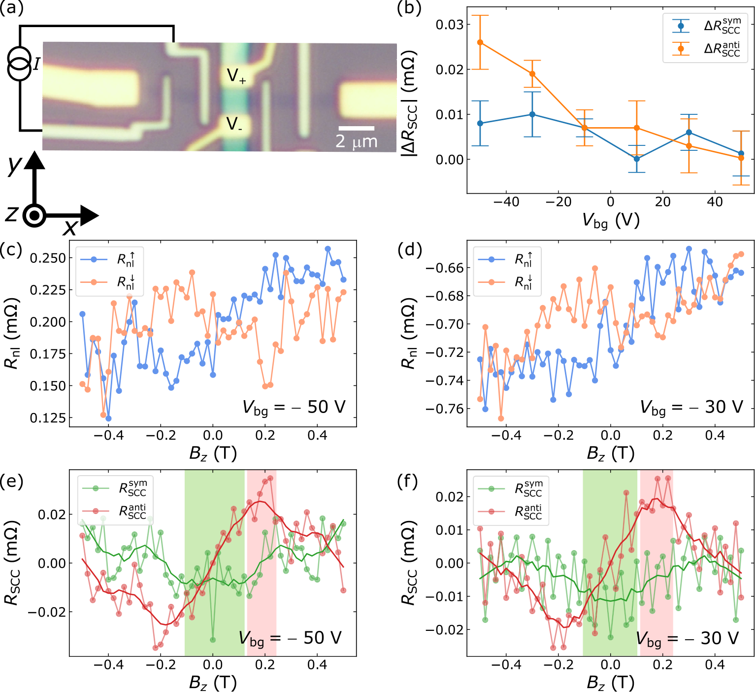
We have also performed SCC experiments in sample 2. In this case, to demonstrate that the -SCC component is indeed due to spin transport, we have applied an out-of-plane magnetic field (). induces spin precession in the plane. As a consequence, -SCC appears as the antisymmetric component in and -SCC as the symmetric one. The results from sample 2 are summarized in Fig. S13. There, one can identify both a symmetric and antisymmetric component in , which show that both - and -SCC components are present in sample 2. This observation confirms that the -SCC component is due to SCC and that both in-plane SCC components are achieved in multiple samples. Another observation we make is that the SCC signal is one order of magnitude smaller than in sample 1, making its observation very challenging. As a consequence, we only observed SCC at 100 K in sample 2. Additionally, for sample 2, we only observed SCC at and V, in contrast with sample 1, where we observed it at positive . We attribute this observation, that is summarized in Fig. S13b, to a different doping of the BLG flake that gives rise to better spin transport for holes than electrons, in contrast with sample 1.
S16 Determination of the rotation angle between bilayer graphene and NbSe2

To determine the rotation angle between the BLG and NbSe2 crystal mirrors, we have assumed that the flakes cleave along a crystallographic axes You et al. 2008. In this case, the alignment between the mirrors can be found by analyzing the optical microscope images of sample 1 and finding the rotation angle between the straight edges. To obtain the edge of the NbSe2 flake in the most accurate way, we have taken the derivative of the image obtained from averaging the red, green and blue channels of the image (Figs. S14a and S14b) and traced its maximum for each value of . Next, we have fit the extracted data to a line (Fig. S14c, where is the horizontal and the vertical coordinate in the image) to obtain its rotation angle with respect to the image using . The confidence interval of has been obtained from the confidence interval of the slope obtained from the fit and assuming that the uncertainty in the determination of the data is its standard deviation from the average value (note that this should lead to a small overestimation due to the small slope of the line). The result from such analysis is .
To determine the rotation angle of the graphene flake with respect to the image, because its contrast is too small and taking the derivative results in a noisy image, we have determined the edges by visual inspection selecting 7 points that we have plotted as a dashed line in Fig. S14a. From the slope of this line, we have determined the angle of the graphene flake (), that is . The confidence interval has been obtained assuming that the uncertainty in is 0.05 m and mm), where 6.8 m is the length of the dashed line. The factor comes from the assumption that the uncertainty in the determination of the different points along the edge is not correlated. The value obtained from a linear fit to all the points coincides with the result extracted from the two extreme values.
Finally, the rotation angle between both flakes has been obtained as .
Similar analysis performed for sample 2 yields a twist angle of .
Note that these values are just an estimate and are only valid if the selected edges correspond to crystal mirrors.
S17 Symmetry considerations
Bulk NbSe2 has space group P63/mmc (194) with corresponding point group 6/mmm (D6h) Lide 2004. Hence, the spin Hall effect (SHE) has only the conventional components, that are given by
| (S16) |
with , where is the spin current density propagating along direction and polarized along Culcer and Winkler 2007; Wimmer et al. 2015; Seemann et al. 2015. is the spin Hall conductivity that relates the charge current density along with the spin current density via SHE.
In bulk NbSe2 there is no Edelstein effect (EE) due to inversion symmetry.
Freestanding monolayer NbSe2 has point group . In this case the SHE still has only conventional components, and the EE is still zero, even though it does not have inversion symmetry.
The surface of bulk NbSe2 (or monolayer NbSe2 on a substrate) has point group . The SHE has an extra component which is not Hall-like (is symmetric in ) Culcer and Winkler 2007; Wimmer et al. 2015; Seemann et al. 2015; Roy et al. 2021. The EE has one term with and the other components are zero. Here, is the induced magnetization, the applied electric field, and the EE tensor converting the electric field into an induced magnetization. For these components, the mirror in is .
The unconventional -SCC component that we want to characterize has and . This means that the unexpected SCC component can be due to an unconventional EE component () or from the SHE component . There is an additional component which is allowed, that is . However, because the signal does not change sign upon reversing the spin diffusion direction along , the latter is not allowed. None of the two possible sources would be allowed even in the less restrictive scenario, that is the surface of bulk NbSe2, thus, we have to break extra symmetries in our device to explain the measured signal.
Bulk NbSe2 with shear strain would have broken , and but preserved and inversion. is allowed in this case, but not because of inversion symmetry Seemann et al. 2015.
The surface of NbSe2 with shear strain has no symmetry left, hence, everything is allowed.
If the mirrors of graphene’s symmetry group and NbSe2 are not aligned, the interface between NbSe2 and graphene does not have any mirror and is allowed without the need for shear strain. Where a Nb or Se atom lies on top of a C atom or a hexagon centre this results in a C3 point group. As explained in the main manuscript, we believe this is the most likely scenario in our devices Li and Koshino 2019; David et al. 2019. In contrast, when the twist angle is 0 or a multiple of 30 degrees, the mirrors are aligned, is not allowed and, where a Nb or Se atom lies on top of a C atom or a hexagon centre, the heterostructure belongs to the C3v point group.