Fermi surface anisotropy in plasmonic metals increases
the potential for efficient hot carrier extraction
Abstract
Realizing the potential of plasmonic hot carrier harvesting for energy conversion and photodetection requires new materials that resolve the bottleneck of extracting carriers prior to energy relaxation within the metal. Using first-principles calculations of optical response and carrier transport properties, we show that directional conductors with Fermi velocities restricted predominantly to one or two directions present significant advantages for efficient hot carrier harvesting. We show that the optical response of film-like conductors, PtCoO2 and Cr2AlC, resemble that of 2D metals, while that of wire-like conductors, CoSn and YCo3B2, resemble that of 1D metals, which can lead to high mode confinement and efficient light collection in small dimensions, while still working with 3D materials with high carrier densities. Carrier lifetimes and transport distances in these materials, especially in PtCoO2 and CoSn, are competitive with noble metals. Most importantly, we predict that carrier injection efficiency from all of these materials into semiconductors can exceed 10% due to the small component of carrier momentum parallel to the metal surface, substantially improving upon the typical less than 0.1% injection efficiency from noble metals into semiconductors.
Keywords:
electron-phonon coupling, anisotropic transport, optical propertiesI Introduction
High-energy electrons and holes excited in metal nanostructures upon the decay of plasmons provide a pathway to leverage light collected efficiently at the nano scale for photochemistry,Linic et al. 2011 imaging,Schuck 2013 and photovoltaic energy conversion.Wang and Melosh 2011 A continuing challenge in plasmonic hot carrier applications is utilizing the excited carriers prior to energy relaxation in the metal,Moskovits 2015; Brongersma et al. 2015 requiring nanostructures smaller than the mean free paths of carriers and material interfaces that are capable of extracting a large fraction of carriers from the metal.Kumar et al. 2021
The field of plasmonic hot carriers has made great strides in expanding the space of materials from noble metals to include refractory plasmonic materialsGuler et al. 2014 such as transition metal nitrides,Patsalas et al. 2018; Ishii et al. 2016; Habib et al. 2018 and low-dimensional materials such as MXenes.Hantanasirisakul and Gogotsi 2018; Velusamy et al. 2019; Jeon et al. 2019 These materials remain stable at smaller dimensions than noble metals, making it possible to minimize energy losses during the transport of carriers across the nanostructure.Habib et al. 2018 Additionally, lower-dimensional plasmonic materials can exhibit higher mode confinement than 3D metals, allowing efficient light capture at smaller length scales.Sundararaman et al. 2020 However, the overall efficiency of extracting hot carriers from plasmonic metals into semiconductors for photovoltaic and photodetection applications remains low, primarily due to the mismatch between carrier momenta near the Fermi energy in metals and the band edges in semiconductors,Chalabi et al. 2014; Tagliabue et al. 2018; Tagliabue et al. 2020a requiring further advances in materials for plasmonic hot carriers.Kumar et al. 2021
Here, we propose that directional conductors – 3D materials that behave like lower-dimensional metals due to Fermi velocities restricted to one or two dimensions – have the potential to simultaneously absorb light efficiently at nanoscale dimensions and inject carriers with high probability into semiconductors. These directional conductors typically have highly anisotropic crystal structures (e.g., layered-materials) which lead to highly anisotropic Fermi surfaces with directional properties. Using first-principles calculations of electronic structure, optical response, electron-phonon and electron-electron scattering, we show that the best directional conductors, including PtCoO2 and CoSn, are competitive with noble metals in their frequency range of plasmonic response and carrier transport distances. We show that their optical response resembles lower-dimensional metals, which may allow the design of plasmonic nanostructures with more efficient light collection at small dimensions than their 3D counterparts. Finally, we show that the lower magnitude of Fermi momenta and the strong directional distribution can be leveraged to greatly enhance the probability of carrier injection into the semiconductor: from below 0.1% typical for noble metals to over 10% for the directional conductors as predicted by a modified Fowler model.
II Methods
II.1 Computational details
We perform electronic structure calculations using the open-source JDFTx software for density-functional theory in the plane wave basis.Sundararaman et al. 2017 We use the Perdew-Burke-Ernzerhof generalized gradient approximation to the exchange correlation functional,Perdew et al. 1996 with non-relativistic ultrasoft Garrity-Bennett-Rabe-Vanderbilt (GBRV) pseudopotentials at kinetic energy cutoffs of 20 Hartrees for the wavefunctions and 100 Hartrees for the charge density.Garrity et al. 2014 We optimize lattice parameters and internal geometries self-consistently for each material, and calculate phonons and electron-phonon coupling from first-principles. The converged lattice parameters have been compared with the corresponding experimental measurements in Table 1. We use a -mesh of 12122 for PtCoO2 and 121212 for Cr2AlC, CoSn, and YCo3B2. For our phonon calculations, we use a -point sampling of 331 for PtCoO2, 332 for Cr2AlC and 333 for CoSn and YCo3B2.
| Material | [Å] | [Å] | |
|---|---|---|---|
| PtCoO2 | 12 | 2.85 (2.82) | 18.03 (17.81) |
| Cr2AlC | 8 | 2.85 (2.86) | 12.75 (12.82) |
| CoSn | 6 | 5.26 (5.28) | 4.26 (4.26) |
| YCo3B2 | 6 | 5.00 (5.04) | 3.04 (3.03) |
We construct maximally localized Wannier functions for each material to accurately reproduce the electronic band structure up to at least 40 eV above the Fermi level, and use them to transform electron and phonon properties using the Wannier module of JDFTx.Souza et al. 2001; Sundararaman et al. 2017 For each of these materials, we use a combination of atomic orbitals and Gaussian orbitals ( Bohr) as the initial guesses or trial orbitals. The Gaussian orbitals are centered at random positions inside the unit cell. We use 5 -orbitals per Pt and Co atom, 1 -orbital and 3 -orbitals per O atom, and 105 Gaussian orbitals for PtCoO2 (159 in total). For Cr2AlC, we use 103 Gaussian orbitals. We use 5 -orbitals per Co and 5 -orbitals and 3 -orbitals per Sn atom, and 100 Gaussian orbitals for the case of CoSn (139 in total). Lastly, for YCo3B2 we use 5 -orbitals per Co, 5 -orbitals and 3 -orbitals per Y atom, 1 -orbital and 3 -orbitals per B atom, and 90 Gaussian orbitals (121 in total). Fig. S3 in the supplemental informationSI shows that the real-space representations of the electronic Hamiltonian, dynamical matrix and electron-phonon matrix elements all decay rapidly with distance,Poncé et al. 2021 falling to of their maximum values by the edge of the corresponding supercells.
Using these, we interpolate electronic energies at wave vector and band , their band velocities and velocity matrix elements , phonon frequencies at wavevector and polarization , and the electron-phonon matrix elements to significantly finer and meshes for integrals over the Brillouin Zone (BZ) in the calculation of optical and carrier transport properties described next.Brown et al. 2016a
II.2 Dielectric functions
We calculate the complex dielectric tensor,
| (1) |
where and are the frequency-independent (static) conductivity tensor and Drude lifetime respectively, is the frequency-dependent momentum relaxation time. The second term captures the Drude response including the effect of phonon-assisted intraband transitions, while the final term captures the effect of direct optical transitions. We evaluate the final term directly using Fermi’s golden rule for the real part,Sundararaman et al. 2014
| (2) |
where is the spin degeneracy factor and are the Fermi occupations of each electronic state. We then evaluate from it using the Kramers-Kronig relation. The energy-conserving -function above is broadened to a Lorentzian due to electron-electron and electron-phonon scattering linewidths, which we also calculate from first principles as described below in Section II.3.Brown et al. 2016a
In the Drude term above (second term of (1)), we account for phonon-assisted transitions within the frequency-dependent momentum relaxation rate,
| (3) |
derived from the Eliashberg spectral function,Allen 1971 and generalized to non-zero temperature.Sundararaman et al. 2020 Here, is the density of electronic states at the Fermi level, and
| (4) |
is the weight of each phonon mode in the ‘transport Eliashberg spectral function’. Above, is the unit cell volume. (The final factor dependent on velocities above accounts for scattering angle compared to the conventional Eliashberg spectral function.Allen 1971) Finally, the numerator in the first term of (1) isSundararaman et al. 2020
| (5) |
which is essentially the generalization of from a spherical Fermi surface to the general anisotropic case.
We apply Monte Carlo sampling with a typical density of -values to fully converge the Brillouin zone integrals above, leveraging the Wannier interpolation of matrix elements. Histogramming the integrands in the above expressions with respect to , we also evaluate the energy distributions of carriers generated upon absorption. See Ref. 28 for further details and demonstration of the quantitative accuracy of this method for conventional plasmonic metals, as well as for low-dimensional and refractory plasmonic materials.Narang et al. 2017; Habib et al. 2018
II.3 Carrier lifetimes and mean free paths
The electron-phonon contribution to the inverse lifetime is given by Fermi’s golden rule as
| (6) |
where the factors in order correspond to energy conservation, occupation factors and the electron-phonon matrix elements. The sum over counts phonon absorption and emission processes. See Ref. 28 and 31 for further details.
The electron-electron contribution is calculated using
| (7) |
where are density matrices in the plane-wave basis with reciprocal lattice vectors , and is the inverse dielectric matrix calculated in the Random Phase Approximation. See Ref. 32 for a detailed introduction to this method and Ref. 28 for our specific implementation details. The only difference from Ref. 28 is the factor , where is the Bose function, which generalizes the approach from to the non-zero temperature formalism.Benedict et al. 2002; Kas and Rehr 2017 In particular, this extension ensures a finite near the Fermi energy as expected for metals,Brown et al. 2016b while the conventional formalism for diverges as .Brown et al. 2016a
The net carrier lifetime is . We use this to calculate the carrier linewidths for the broadening of the energy conservation factors above, as well as for the mean free path . Note that as in previous theoretical studies,Brown et al. 2017; Habib et al. 2018 the carrier lifetime calculated here is the time for individual electron-phonon scattering events. This is distinct from the electron-phonon fall/decay time often reported in pump-probe spectroscopy.Su et al. 2019; Tomko et al. 2021; Hattori et al. 2021 The electron-phonon relaxation time reported in experiments is the time constant for energy transfer from the electronic subsystem to the phononic subsystem.
II.4 Interfacial injection probability
We estimate probability of injecting carriers into semiconductors using a modified Fowler model that accounts for the electronic structure of the metal by directly employing band momenta computed from DFT (and interpolated using Wannier functions).Tagliabue et al. 2018; Tagliabue et al. 2020b; Tagliabue et al. 2020a Specifically, for each electronic state in the metal, we decompose the momentum into a component along the interface normal direction (assumed to be the preferred transport direction ), , and a component parallel to the interface, .
The modified Fowler model matches the parallel component, requiring . Assuming a parabolic band structure for the semiconductor, the corresponding interface-normal component of the momentum is
| (8) |
where is the Heaviside step function, and are the effective masses and Schottky barrier heights of electrons/holes in the semiconductor. Note that states that are not allowed to enter the semiconductor lead to .
Finally, the probability of injection in the modified Fowler model, accounting for a transmission matrix element due to momentum mismatch,Chalabi et al. 2014 is
| (9) |
In our analysis in section III.5, we report the average injection probability at each carrier energy,
| (10) |
where is the electronic density of states.
III Results and Discussion
III.1 Directional conductors
We recently identified several directional conductors that exhibit promise for conduction in nanoscale geometries using a high-throughput screening based on electronic structure calculations.Kumar et al. 2022 These materials fall into two broad classes, film-like and wire-like conductors, which exhibit excellent transport in two perpendicular directions and along a single axis respectively. To investigate the potential of directionality to additionally enhance harvesting of hot carriers far from equilibrium, we select two representative materials from each class. In particular, for the film-like conductors, we select the delsafossite oxide PtCoO2 with the lowest resistivity and the well-studied MAX phase Cr2AlC, while for the wire-like conductors, we select the two most conductive materials, CoSn and YCo3B2.

Figure 1 shows the unit cell structure and Fermi surfaces for all four materials. PtCoO2 exhibits an almost perfect hexagonal-prism-shaped Fermi surface, which leads to all the Fermi velocities directed in the hexagonal plane of the materialEyert et al. 2008. This leads to an in-plane resistivity, along the preferred transport direction , that is smaller than the out-of-plane resistivity along the preferred surface normal direction (Table 2). Such large anisotropies have been reported for transport properties of two-dimensional materials like graphene,Pop et al. 2012 attributed to the weak van der Waals coupling between layers. However, all directional materials we investigate here are 3D crystals with strong bonding in all directions (Fig. 1). Cr2AlC also has similar Fermi surface orientations and preferred transport directions, but a much weaker anisotropy in the resistivityBugnet et al. 2014.
| Type | Material | [cm] | |||
|---|---|---|---|---|---|
| Along | Along | ||||
| Film-like | PtCoO2 | 1.8 | 5960 | ||
| Cr2AlC | 14.5 | 47.8 | |||
| Wire-like | CoSn | 2.9 | 37.2 | ||
| YCo3B2 | 5.7 | 37.9 | |||
The remaining two materials, CoSn and YCo3B2, have Fermi surface sheets parallel to the hexagonal plane (Fig. 1(c-d)), leading to Fermi velocities and conduction predominantly along the axis (Table 2). These materials therefore have a single preferred transport direction, with two preferred surface normal directions, making them suitable for conduction in nanoscale wires.Kumar et al. 2022 To discuss these film-like and wire-like materials on a similar footing, we will henceforth refer to properties along preferred transport direction and along the preferred normal direction , but note that the crystallographic orientation of these directions is different for the two classes of materials as specified in Table 2.
Finally, note that the resistivity for all these conductors, except for the Cr2AlC max phase, is comparable to that for the most common plasmonic metals: 1.6, 1.7, 2.3 and 2.8 cm for silver, copper, gold and aluminium,Brown et al. 2016a while the resistivity is much larger. This difference for Cr2AlC can be understood by comparing the electronic structures of the four materials (see Fig. S1 in supplemental materialSI. In Cr2AlC, the states near the Fermi level are dominated by -bands Ito et al. 2017 which tend to be narrower and hence, have smaller velocities and larger density of states at the Fermi level. The other three materials studied here (PtCoO2, YCo3B2 and CoSn) have larger Fermi velocities and smaller density of states due to larger dispersion of the bands crossing the Fermi level. Consequently, Cr2AlC exhibits higher electron-phonon scattering rates with more states to scatter into, leading to overall worse transport properties including bulk resistivity, carrier lifetimes and mean free paths.
III.2 Optical response
To investigate the suitability of these materials for plasmonic applications, we first consider their Drude response. Figure 2 shows the calculated transport Eliashberg spectral functions (Section II.2) and corresponding frequency-dependent Drude momentum relaxation times due to electron-phonon scattering. The electron-phonon coupling at the Fermi level is weakest for PtCoO2, as indicated by the lowest spectral function magnitude in Fig. 2(a), followed by CoSn, YCo3B2 and finally Cr2AlC. Correspondingly, the Drude relaxation time at low frequencies drops from fs for PtCoO2 to fs for YCo3B2, in the same order.
With increasing frequency, Drude relaxation can access higher energy phonon modes that were inaccessible using thermal energy at room temperature alone, causing to decrease. For PtCoO2, decreases from 60 fs at low frequency to 54 fs at optical frequencies, remaining larger than the low-frequency relaxation time for most elemental metals! The largest proportional drop in is from 15.6 fs to 11 fs for Cr2AlC, which has the highest-energy phonon spectrum, while the smallest drop in is from 31 fs to 28 fs for CoSn with the lowest-energy phonon spectrum.
The decrease in with frequency accounts for phonon-assisted transitions along with the Drude term,Sundararaman et al. 2020 which we then combine with predictions of direct transitions (Section II.2) to compute the overall complex dielectric functions shown in Fig. 3. Note that the dielectric functions are highly anisotropic, with qualitative differences between the and directions for these directional conductors. In particular, the plasmonic window – the region with is much larger along the direction than the direction. The plasmonic window of PtCoO2, CoSn, and YCo3B2 each extend above 2.5 eV along , surpassing the plasmonic range of gold (2.6 eV) and approaching that of silver (3.4 eV).Brown et al. 2016b In contrast, the plasmonic window along is below 0.5 eV for all four materials, with that of PtCoO2 (the most anisotropic of the four) being virtually negligible.

Additionally, along the preferred transport directions are relatively low when Re crosses zero, indicating plasmonic response with quality factors comparable to noble metals, most notably for CoSn. In the plasmonic frequency range for , most of these materials exhibit dielectric-like behavior, , along the direction. Consequently, these materials essentially behave like lower-dimensional materials optically – the film-like conductors like 2D materials and the wire-like conductors like 1D materials, but we emphasize again that these materials are 3D crystals bonded strongly in all directions. This opens up the possibility to reap the advantages of low-D plasmonics, such as high confinement,Sundararaman et al. 2020 while working with easier-to-process 3D materials. See the supplemental material for tables of predicted dielectric functions to facilitate design of plasmonic structures using these materials;SI we focus here instead on material properties including hot carrier distributions and transport next.
III.3 Hot carrier generation
Plasmon decay is captured by the imaginary part of the dielectric functions, , and the energy lost by the plasmon is deposited in an electron-hole pair. Figure 4 shows the energy distribution of hot carriers excited upon plasmon decay, calculated by resolving contributions to by carrier energy (Section II.2).Brown et al. 2016a Unlike a clear separation between phonon-assisted transitions below an interband threshold and direct transition above it in typical plasmonic metals,Brown et al. 2016a; Habib et al. 2018 these complex conductors exhibit direct transitions at almost all plasmon frequencies. Only PtCoO2 and CoSn show a small frequency range ( eV) where indirect phonon-assisted transitions contribute significantly. Interestingly, the relative importance of phonon-assisted transitions in PtCoO2 is enhanced along the direction, indicating a selection rule that the lowest energy direct transitions are allowed only for in-plane electric fields in this material.
The predominance of direct transitions leads to relatively complex energy distributions of carriers, sensitive to details in the electronic structure. Consequently, Figure 5 shows moments of these carrier distributions, indicating the fraction of (indirect) intraband transitions and the distribution of energy between electrons and holes. Direct transitions dominate above 1 eV, with the intraband fraction dropping below 20%, in all four materials. Additionally, despite the complex and different structure in the electron and hole distributions in Fig. 4, the overall energy separation between electrons and holes is approximately even, with between 40 and 60% of the energy in the electrons, across the frequency range considered for all materials. The only notable deviation is that 80% of the energy is deposited in the electrons by intraband transitions in PtCoO2 for polarization, while the energy split is close to equal even in that energy range for the polarization. Overall, given the absence of systematic asymmetries in electron and hole distributions, such as those for noble metals,Brown et al. 2016a analyses of hot carriers in these directional conductors may safely assume a uniform electron and hole energy distribution extending from 0 to the plasmon energy, independent of polarization.
Note that the hot carrier properties presented here are calculated for bulk materials. Since surface sites (like edges, facets and corners) and shape and size of the nanoparticles can significantly enhance the rate and distribution of hot carrier generation,Rossi et al. 2020 future studies should focus on the effect of atomic structure on plasmonic properties of these directional conductors. Additionally, nanoparticle shapes and surface characteristics will vary dramatically depending on the synthesis approach, and present additional opportunities in targeting techniques such as self-organized nanodecompositionDietl et al. 2015 towards nanoparticles suitable for hot carrier extraction in future work.
III.4 Carrier transport

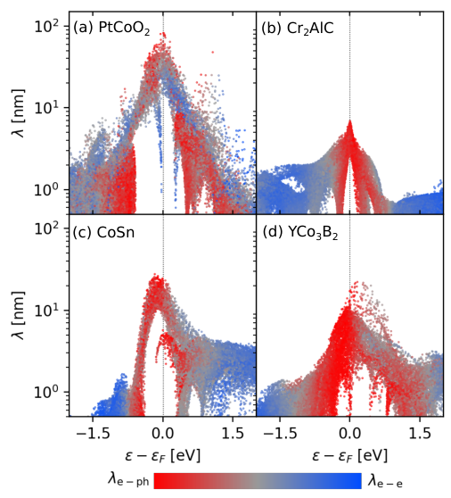
Efficient hot carrier harvesting requires extraction of the carriers from the metal prior to thermalization by electron-phonon and electron-electron scattering. Figures 6 and 7 respectively show the predicted lifetime and mean free path of hot carriers in the directional conductors, accounting for both these scattering mechanisms (Section II.3). Electron-phonon scattering dominates near the Fermi energy, while the phase-space for electron-electron scattering increases with increasing electron or hole energies and eventually dominates over electron-phonon scattering, exactly analogous to the case for other plasmonic metals including elemental metals and transition metal nitrides.Brown et al. 2016a; Habib et al. 2018 The mean free paths drop off with energy more quickly than the life times in most of the materials, especially for the holes, indicating a reduction in average carrier velocities for energies far from the Fermi level.
The peak carrier lifetimes and mean free paths in these materials are competitive with noble metals, especially in PtCoO2 and CoSn. However, the drop-off with energy is faster in these materials compared to noble metals, with mean-free paths dropping below 10 nm for carriers with 1 eV energies for all all four materials. This is partly because the directionality of electronic structure is a feature restricted to a narrow energy window surrounding the Fermi energy, with a marked increase in density of states away from the Fermi energy (Figure S1 in Supplemental MaterialSI), leading to a corresponding increase in pase space for scattering for higher energy carriers. This indicates the need to carefully design plasmonic geometries to minimize the average distance between the location of carrier generation and the interfaces where carriers can be collected to below 10 nm.
III.5 Carrier injection across interfaces
The final step in hot carrier harvesting is transferring the carriers across an interface, such as a metal-semiconductor interface, prior to energy relaxation in the metal. This step is typically the largest limiting factor in hot carrier collection efficiency because most carriers in the metal encounter total internal reflection at the interface with the semiconductor, as captured by the semi-classical Fowler model of carrier injection.Chalabi et al. 2014; Kumar et al. 2021 In particular, the injection from noble metals into semiconductors at energies just above the Schottky barriers is typically % or smaller due to the large mismatch between the Fermi velocity in the metal and velocities near the band edges of the semiconductor.Tagliabue et al. 2018 Injection from lower-velocity bands of the metal, such as -bands in copper, can slightly increase these probabilities, but they remain at that small order of magnitude.Tagliabue et al. 2020a
The directional conductors investigated here have the potential to remedy this issue in two ways. First, the Fermi velocity in these materials is lower than in noble metals, exhibiting a slightly better match to velocities near semiconductor band edges. Second, the directionality of the velocity makes it possible to substantially reduce the component parallel to the surface (that needs to match across the interface) by collecting in an interface whose normal is along .
Figure 8(a) shows that the component of carrier velocity direction along is close to 1 for wire-like conductors CoSn and YCo3B2, indicating that the remaining components must be much smaller. This projection is smaller for the film-like conductors, which have large velocity components along two orthogonal directions, and approaches the isotropic limit of 1/2 for a noble metal like gold. Figures 8(b-c) show that this directionality of the velocity indeed leads to a significantly larger injection probability than for the case of gold, as predicted using a modified Fowler model (Section II.4). Compared to in gold, all directional conductors have the potential to inject with probability into a model semiconductor (assuming a typical electron and hole mass of 0.3 for simplicity), presenting significant opportunities for efficient plasmonic hot carrier harvesting.
IV Conclusions
Using first-principles calculations of optical response, carrier generation, transport and injection, we show the significant promise of directional conductors for plasmonic hot carrier applications. The strong anisotropy of Fermi velocity in these materials to one or two directions introduces 1D wire-like or 2D film-like behavior in a 3D-crystalline material. These materials exhibit plasmonic response over a range of frequencies comparable to noble metals along the preferred transport direction(s) , while simultaneously exhibiting dielectric behavior in the preferred normal direction(s) at those frequencies, mimicking the optical response of a lower-dimensional metal. Hot carrier generation and transport are also similar to noble metals, but directionality in the momenta shows promise for orders of magnitude higher efficiency in extraction of hot carriers from these materials into semiconductors. The dielectric functions, carrier transport and injection models reported here can now be used to design plasmonic nanostructures with the potential for high-efficiency hot carrier harvesting.
Acknowledgements
The authors acknowledge funding from SRC under Task No. 2966.002. Calculations were carried out at the Center for Computational Innovations at Rensselaer Polytechnic Institute.
References
- Linic et al. (2011) S. Linic, P. Christopher, and D. B. Ingram, Nature Mater. 10, 911 (2011).
- Schuck (2013) P. J. Schuck, Nature Nanotech. 8, 799 (2013).
- Wang and Melosh (2011) F. Wang and N. A. Melosh, Nano Lett. 11, 5426 (2011).
- Moskovits (2015) M. Moskovits, Nature Nanotech. 10, 6 (2015).
- Brongersma et al. (2015) M. L. Brongersma, N. J. Halas, and P. Nordlander, Nature Nanotech. 10, 25 (2015).
- Kumar et al. (2021) S. Kumar, A. Habib, and R. Sundararaman, Trends Chem. 3, 902 (2021).
- Guler et al. (2014) U. Guler, A. Boltasseva, and V. M. Shalaev, Science 344, 263 (2014).
- Patsalas et al. (2018) P. Patsalas, N. Kalfagiannis, S. Kassavetis, G. Abadias, D. V. Bellas, C. Lekka, and E. Lidorikis, Mater. Sci. Eng. R Rep. 123, 1 (2018).
- Ishii et al. (2016) S. Ishii, S. L. Shinde, W. Jevasuwan, N. Fukata, and T. Nagao, ACS Photon. 3, 1552 (2016).
- Habib et al. (2018) A. Habib, F. Florio, and R. Sundararaman, J. Opt. 20, 064001 (2018).
- Hantanasirisakul and Gogotsi (2018) K. Hantanasirisakul and Y. Gogotsi, Adv. Mater. 30, 1804779 (2018).
- Velusamy et al. (2019) D. B. Velusamy, J. K. El-Demellawi, A. M. El-Zohry, A. Giugni, S. Lopatin, M. N. Hedhili, A. E. Mansour, E. D. Fabrizio, O. F. Mohammed, and H. N. Alshareef, Adv. Mater. 31, 1807658 (2019).
- Jeon et al. (2019) J. Jeon, H. Choi, S. Choi, J.-H. Park, B. H. Lee, E. Hwang, and S. Lee, Adv. Func. Mater. 29, 1905384 (2019).
- Sundararaman et al. (2020) R. Sundararaman, T. Christensen, Y. Ping, N. Rivera, J. D. Joannopoulos, M. Soljačić, and P. Narang, Phys. Rev. Mater. 4, 074011 (2020).
- Chalabi et al. (2014) H. Chalabi, D. Schoen, and M. L. Brongersma, Nano Lett. 14, 1374 (2014).
- Tagliabue et al. (2018) G. Tagliabue, A. Jermyn, R. Sundararaman, A. Welch, J. DuChene, R. Pala, A. Davoyan, P. Narang, and H. Atwater, Nature Commun. 9, 3394 (2018).
- Tagliabue et al. (2020a) G. Tagliabue, J. S. DuChene, A. Habib, R. Sundararaman, and H. A. Atwater, ACS Nano 14, 5788 (2020a).
- Sundararaman et al. (2017) R. Sundararaman, K. Letchworth-Weaver, K. Schwarz, D. Gunceler, Y. Ozhabes, and T. A. Arias, SoftwareX 6, 278 (2017).
- Perdew et al. (1996) J. P. Perdew, K. Burke, and M. Ernzerhof, Phys. Rev. Lett. 77, 3865 (1996).
- Garrity et al. (2014) K. F. Garrity, J. W. Bennett, K. M. Rabe, and D. Vanderbilt, Comput. Mater. Sci. 81, 446 (2014).
- Kushwaha et al. (2015) P. Kushwaha, V. Sunko, P. J. Moll, L. Bawden, J. M. Riley, N. Nandi, H. Rosner, M. P. Schmidt, F. Arnold, E. Hassinger, et al., Science Advances 1, e1500692 (2015).
- Lin et al. (2005) Z. Lin, Y. Zhou, M. Li, and J. Wang, International Journal of Materials Research 96, 291 (2005).
- Meier et al. (2020) W. R. Meier, M.-H. Du, S. Okamoto, N. Mohanta, A. F. May, M. A. McGuire, C. A. Bridges, G. D. Samolyuk, and B. C. Sales, Physical Review B 102, 075148 (2020).
- Kowalczyk (2000) A. Kowalczyk, physica status solidi (b) 218, 495 (2000).
- Souza et al. (2001) I. Souza, N. Marzari, and D. Vanderbilt, Phys. Rev. B 65, 035109 (2001).
- (26) See supplemental information at [URL will be inserted by publisher] for electron and phonon band structures, supercell convergence of real-space representations of matrix elements, tables of predicted dielectric functions, spectral functions and injection probabilities.
- Poncé et al. (2021) S. Poncé, F. Macheda, E. R. Margine, N. Marzari, N. Bonini, and F. Giustino, Physical Review Research 3, 043022 (2021).
- Brown et al. (2016a) A. M. Brown, R. Sundararaman, P. Narang, W. A. Goddard, and H. A. Atwater, ACS Nano 10, 957 (2016a).
- Sundararaman et al. (2014) R. Sundararaman, P. Narang, A. S. Jermyn, W. A. Goddard III, and H. A. Atwater, Nat. Commun. 5, 5788 (2014).
- Allen (1971) P. B. Allen, Phys. Rev. B. 3, 305 (1971).
- Narang et al. (2017) P. Narang, L. Zhao, S. Claybrook, and R. Sundararaman, Adv. Opt. Mater. 5, 1600914 (2017).
- Ladstädter et al. (2004) F. Ladstädter, U. Hohenester, P. Puschnig, and C. Ambrosch-Draxl, Phys. Rev. B 70, 235125 (2004).
- Benedict et al. (2002) L. X. Benedict, C. D. Spataru, and S. G. Louie, Phys. Rev. B 66, 085116 (2002).
- Kas and Rehr (2017) J. J. Kas and J. J. Rehr, Phys. Rev. Lett. 119, 176403 (2017).
- Brown et al. (2016b) A. M. Brown, R. Sundararaman, P. Narang, W. A. Goddard III, and H. A. Atwater, Phys. Rev. B 94, 075120 (2016b).
- Brown et al. (2017) A. M. Brown, R. Sundararaman, P. Narang, A. M. Schwartzberg, W. A. Goddard III, and H. A. Atwater, Physical review letters 118, 087401 (2017).
- Su et al. (2019) M.-N. Su, C. J. Ciccarino, S. Kumar, P. D. Dongare, S. A. Hosseini Jebeli, D. Renard, Y. Zhang, B. Ostovar, W.-S. Chang, P. Nordlander, et al., Nano Letters 19, 3091 (2019).
- Tomko et al. (2021) J. A. Tomko, S. Kumar, R. Sundararaman, and P. E. Hopkins, Journal of Applied Physics 129, 193104 (2021).
- Hattori et al. (2021) Y. Hattori, J. Meng, K. Zheng, A. Meier de Andrade, J. Kullgren, P. Broqvist, P. Nordlander, and J. Sá, Nano letters 21, 1083 (2021).
- Tagliabue et al. (2020b) G. Tagliabue, J. S. DuChene, M. Abdellah, A. Habib, D. J. Gosztola, Y. Hattori, W.-H. Cheng, K. Zheng, S. E. Canton, R. Sundararaman, J. Sá, and H. A. Atwater, Nature Mater. 19, 1312 (2020b).
- Kumar et al. (2022) S. Kumar, C. Multunas, B. Defay, D. Gall, and R. Sundararaman, Phys. Rev. Materials 6, 085002 (2022).
- Eyert et al. (2008) V. Eyert, R. Frésard, and A. Maignan, Chemistry of Materials 20, 2370 (2008).
- Pop et al. (2012) E. Pop, V. Varshney, and A. K. Roy, MRS bulletin 37, 1273 (2012).
- Bugnet et al. (2014) M. Bugnet, M. Jaouen, V. Mauchamp, T. Cabioc’h, and G. Hug, Physical Review B 90, 195116 (2014).
- Ito et al. (2017) T. Ito, D. Pinek, T. Fujita, M. Nakatake, S.-i. Ideta, K. Tanaka, and T. Ouisse, Physical Review B 96, 195168 (2017).
- Rossi et al. (2020) T. P. Rossi, P. Erhart, and M. Kuisma, ACS nano 14, 9963 (2020).
- Dietl et al. (2015) T. Dietl, K. Sato, T. Fukushima, A. Bonanni, M. Jamet, A. Barski, S. Kuroda, M. Tanaka, P. N. Hai, and H. Katayama-Yoshida, Rev. Mod. Phys. 87, 1311 (2015).