2021
Monte Carlo simulations have been performed for 855 MeV and 6.3 GeV electrons channeling in silicon single crystals at circular bent (111) planes. The aim was to identify critical experimental parameters which effect the volume-deflection and volume-capture characteristics. To these belongs the angular alignment of the crystal with respect to the nominal beam direction. The continuum potential picture has been utilized. The simulation results were compared with experiments. It turns out that the assumption of an anticlastic bending of the crystal, bent on the principle of the quasi-mosaic effect, is not required to reproduce the experimental observations.
Beam steering with quasi-mosaic bent silicon single crystals
keywords
PACS 61.85.+p, PACS 41.75.Ht, PACS 02.70.Uu1 Introduction
The understanding of the de-channeling process in bent single crystals is of utmost importance, not only for particle steering in high energy physics but also for the construction of compact radiation sources in the MeV range and beyond, for an overview see e.g. Korol et al. KorS14. In all cases bent crystals are required the production of which are based on different principles. The quasi-mosaic effect has been proven as beneficial to achieve a curvature of certain plains of single crystals which otherwise would be flat CamG15. A number of experiments utilized this effect to steer charged particles at (111) planes of silicon single crystals. For the current work the experimental publications MazB14; WieM15; WisU16 are of particular importance in which the results of deflection studies for 855 MeV and 6.3 GeV electrons have been described.
It is well known that at bending employing the quasi-mosaic effect a (parasitic) anticlastic bending is connected which must be minimized CamG15; GuiM09. If it is significant, the beam steering pattern may alter as function of the anticlastic bending radius, the beam divergence and spot size, as well as its lateral displacement with respect to the center of the spherical calotte. Such effects were recently investigated on the basis of simulation calculations with the MBN explorer software package by Sushko et al. SusK21 suggesting that the beam profiles measured in the SLAC experiment WieM15; WisU16 cannot be understood without the introduction of an anticlastic bending.
In this contribution some key experimental results obtained for silicon single crystals were reinvestigated by means of Monte Carlo simulations with a computer code utilizing the well known continuum potential picture of Lindhard Lin65. The latter has been exploited by a number of authors, for an overview see, e.g., Korol et al. (KorS21, Chapter 2). In particular the DYNECHARM++ code of Bagli and Guidi BagG13, and CRYSTALRAD of Sytov et al. SytT19 should be mentioned. The continuum potential picture has the advantage that channeling can be classically understood for ultra-relativistic particles in a rather intuitive manner. The current work is based on the paper of Backe Bac22 in which details of the underlying formalism are described on the example of channeling of 855 MeV electron in (110) planes of diamond.
The basic ingredients of the model are summarized in the following section 2. Section 3 is devoted to the Monte Carlo simulations of the beam profiles. The results are compared with the experimental observations of beam profile measurements MazB14; WieM15; WisU16, and discussed in section 4 with regard to a possible anticlastic bending. The paper closes in section 5 with conclusions. For the purpose of a check of the reliability of the code, in Appendix 7 simulation calculations are presented for the transition rate as function of the penetration depth and compared with experimental results.
2 Continuum potential and scattering distributions
For the calculation of the channeling potential, as well as the angular distribution of the scattered electrons, the Molière representation for the electronic scattering factors Mol47 was used, however, with the modified parameters for silicon
| (1) |
Here are the Thomas-Fermi screening factor with the Bohr radius, and =14 for silicon. This parameter set approximates the six-parameter Doyle-Turner representation quoted by Chouffani and Überall ChoU99, see Fig. 1, to better than 8% in the full range of . The quantity is related to the momentum transfer by , with the momentum of the particle, its velocity, the speed of light, and the scattering angle.
The potential has been calculated according to the textbook of Baier et al. (BaiK98, chapter 9.1). The result is shown in Fig. 2 together with the positive and negative charge densities and , respectively, across the channel. The latter has been derived from the plane potential with the aid of the one dimensional Poisson equation.
The normalized scattering distribution functions for electron-atom interactions at energies of 855 MeV and 6.3 GeV, respectively, are
| (2) | |||||
| (3) | |||||
with the projected scattering angle. The numerical parameters are related to the Molière parameters of Eq. (2) in a rather involved manner. The distribution functions are depicted in Figs. 3 and 4, full curves.
The scattering distributions for electron-electron collisions have also been calculated according to Bac22, for some details see Appendix 6. The results are included in Figs. 3 and 4 as dot-dashed lines. These distributions can be approximated by the heuristic function11 1 For electrons with an energy of 855 MeV the parameters are = 3.5 , , and , and for the energy of 6.3 GeV = 6.7 , , and . The approximations are better than about 10 % in the interval 0.1 rad 10 mrad and 0.1 rad 5 mrad for 855MeV and 6300 MeV, respectively. Below the lower and above the upper limits the approximations are significantly worse.
| (4) |
3 Simulation calculations
Based on the scattering distributions derived in the last section, simulation calculation have been performed for (111) planar channeling of 855 and 6.3 GeV electrons in silicon single crystals. Details of the simulation procedure are described in the paper Bac22. For the former energy the crystal had a thickness of 30.5 m and a bending radius of = 33.5 mm, for the latter 60 m and = 150 mm. In both cases experimental results are available MazB14; WisU16 with which the simulation calculations will be compared. The reliability of the formalism was checked with results for the rate distribution as function of the penetration depth from which de-channeling lengths were derived for a comparison with literature, see appendix 7.
3.1 Sensitive parameters for the shape of beam profiles
Of crucial importance for the shape of the beam profiles is the initial occupation probability as function of the transverse energy . As shown in Fig. 5 it strongly depends on the alignment of the crystal with respect to the beam direction, i.e., on the entrance angle into the crystal. A uniform distribution of the electron density across the transverse coordinate was assumed, and for the angular distribution a Gaussian with standard deviations = 8.0 rad, as conjectured from the information given by Wienands et al. WieM15.
In addition, sensitive parameters are the anticlastic bending radius, and a misalignment of the electron beam with respect to the spherical calotte representing the anticlastic deformation. Nearly no experimental information was provided in the publications except that the anticlastic bending was minimized at the production of the crystals. Significant effects on the beam profile for the SLAC experiment are expected for an anticlastic bending radius less than 10 m, assuming for spot size and divergence the upper limits of 150 m and 10 rad, respectively.
Initially, an anticlastic bending will be neglected in the analysis. If the experimental observations can not be reproduced, in a second step assumptions on the anticlastic bending radius, on the beam spot (size, divergence, displacement) can be made in order to improve the simulation results.
3.2 Beam profiles for the MAMI experiment at 855 MeV
The simulated beam profiles for 855 MeV electrons steered in (111) planes of the silicon single crystal are shown in Fig. 6, together with experimental results taken from Mazzolari et al. MazB14. A good overall agrement can be stated. In particular, the deflection peaks due to channeling, as well as the volume reflection shift in opposite direction for the tilted crystal are well reproduced. Merely, the intensity of the volume reflected peak seems slightly lower than the measurement, and the shift a little bit larger. It should be stressed that no change has been observed in the simulation calculations within the statistical errors if an anticlastic bending radius of 3.66 m GuiM09 was assumed.


3.3 Beam profiles for the SLAC experiment at 6.3 GeV
Fig. 7 depicts simulated beam profiles and experimental results for 6.3 GeV electrons steered with bent (111) planes of the silicon single crystal. Several interesting features can be recognized. For the spectrum shown in Fig. 7 (d) the crystal is de-tuned already by -60 rad towards the amorphous domain. The main peak is situated close at the deflection angle = 0 mrad, and the re-channeling peak appears shifted to 0.46 mrad, the geometrically expected angle. Its intensity is already rather weak. Increasing the de-tuning angle, the re-channeling peak shifts and reaches the nominal value of = 0.4 mrad at = 0 rad as expected. Thereby its intensity increases gradually since more and more electrons will be captured at the crystal entrance into the channel. In panels (f)-(h) simulation calculations for positive de-tuning angles are depicted. The main peak is shifted towards negative deflection angles . This is the well known volume reflection.
Let us compare the simulation calculations with the experimental result shown in panel (a) of Fig. 7. The measured beam profile agrees quite well with the simulation calculation shown in panel (c) for = -30 rad, and not for = 0 rad, see black curve which is the experimental result shown in panel (a). The simplest explanation for this finding is that the nominal angular directions in experiment and simulation are differently defined, or in other words, that the crystal is de-tuned with respect to the nominal beam direction. This conjecture is corroborated by means of Fig. 7, panel (g). The measurement agrees best with the simulation at 170 rad, and not at 200 rad, panel (f), indicating again the de-tuning angle of 30 rad. A fine-tuning of has not been done.
The intensity of the simulated structure for volume capture appears to be somewhat larger than the measurement indicate, see Fig. 7, panel (g). Also the volume deflection peak is not exactly reproduced by the simulation calculations. It is in comparison to the experiment, black curve, slightly shifted. The reason for these deviations is not quite clear. It may indicate a deficiency of the simulation model. If the particle trajectory approaches the tangent of a bending plane, the effects of the volume-deflection and volume-capture are particularly sensitive to the shape of the electric potential.
The probability density of the deflected particles in Fig. 7 (b) for the crystal in the channeling orientation at = 0 rad does not agree with the result obtained with the aid of the DYNECHARM++ simulation by Wienands et al. (WieM15, Fig. 3). The channeling peak appears at about 430 and not at 400 rad as expected. Apparently the calculations were performed with a de-tuning angle close to 30 rad which was defined as ”channeling orientation”. Indeed, good agreement is found with our simulation calculation under this assumption.
4 Discussion
For the MAMI experiment at 855 MeV Monte Carlo simulations results are depicted in Mazzolari et al. (MazB14, Fig. 3) which were made with a code of Baryshevski and Tikhomirov BarT13. Nearly perfect agreement with the experimental observation was found for both, alignments of the crystal into the channeling regime ( = 0), and for the volume capture situation ( = 450 rad). A detailed analysis of the same experiment was performed by Haurylavets et al. HaL22 an the basis of the MBN explorer software package under various sophisticated assumptions. Results are shown in Fig. 6 suggesting that scattering might be overestimated. The authors mention that a possible reason for the discrepancies can be associated with the Moliére parametrization which describe the electron–atom interaction. Indeed, Fig. 1 shows that the original Moliére parametrization overestimates for small momentum transfers the scattering factors obtained with the Doyle-Turner approach. This fact influences also the shape of the potential, at least in our continuum potential picture. However, simulation calculations with the original Moliére parameters revealed that this way the differences can not be explained.
For the SLAC experiment at 6.3 GeV WisU16 Sushko et al. SusK22 explained the beam profile with the aid of an anticlastic bending of the crystal. Parameter sets for the size of the beam spot, its displacement and the radius of the anticlastic curvature are presented at which the simulations are in accord with the experimental observation. Their Fig. 2 allows approximately a comparison with our results. The simulation is done for a relatively narrow beam with = 75 m in comparison with the displacement of = 675 m for which a good agreement with the experimental result is obtained. Utilizing their Eqns. (2) and (3) for = 400 rad and an anticlastic bending radius = 300 cm, the entrance angle is = 25 rad. The latter is in fair agreement with our finding without the assumption of an anticlastic bending, however, instead for a de-tuning angle of 30 rad of the crystal with respect to the beam direction.
5 Conclusions
In this contribution Monte Carlo simulation results for electron beam deflections in quasi-mosaic bent (111) planes of silicon single crystals were compared with experimental results. The continuum potential picture has been utilized. For the 855 MeV experiment at MAMI good agreement between simulation calculations and the experimental observation was found. For the SLAC experiment at 6.3 GeV the entrance angle into the planes turns out to be a rather sensitive parameter. Small de-tuning angles in the order of some tenth of rad’s perturb significantly the intensity ratio between transmitted and channeled particles with the consequence, that an anticlastic bending is not necessary to explain the gross properties of the experimental observation. However, it can not be excluded that in an second order approach the remaining small deviations visible in Fig. 7, panels (c) and (g), may require it.
Anyway, in the sense of Occam’s razor this simpler explanation should be preferred.
Acknowledgements
I would like to express my gratitude to José M. Fernández-Varea to provide me with numerical data of H. Bichsel Bic88 for the optical oscillator strength (OOS) of silicon.
Fruitful discussions with A. V. Korol, W. Lauth, A. V. Solov’yov, A. Mazzolari, and A. Sytov are gratefully acknowledged.
Declarations
This work has been financially supported by the European Union’s Horizon 2020 research and innovation programme – the N-LIGHT project (GA 872196) within the H2020-MSCA-RISE-2019 call.
6 Differential cross-sections for scattering at electrons
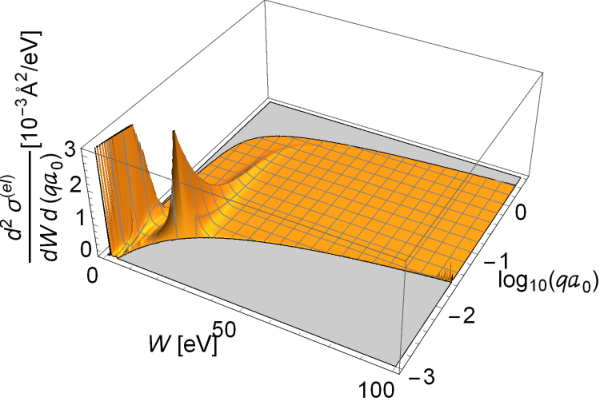
The low energy part of the double differential cross-section at scattering on atomic electrons is shown in Fig. 8.
The energy differential cross-sections as function of the energy loss and momentum transfer are obtained after proper integration over the kinematical allowed and the kinematical allowed , respectively. The results are shown in Fig. 9.
7 Simulation of de-channeling rates
For the purpose of a check with otherwise obtained results, simulation calculations for the transition rate as function of the penetration depth were performed for planar (111) channeling of electrons with an energy of 6.3 GeV from which the de-channeling length was derived. De-channeling is signaled if the electron leaves the potential boundaries, the crystal after 200 m, or if it reaches the maximum transverse energy for which 20 = 452 eV was chosen. Fig. 10 show results. In panels (b) and (d) instantaneous transition rates
| (5) |
are presented as derived from the simulated channel occupation numbers and the channel occupation depicted in panels (a) and (c). For less than about 14 m the instantaneous transition rates are larger than the constant mean value for 14 m.
For 855 MeV, see Fig. 10 left panel, the simulated de-channeling rate 1/ = (15.4 0.3) m is in fair agreement with the value 13.6 m quoted by Mazzolari et al. (MazB14, Table I). However, the latter is not based on pure experimental observations but relies also on simulation calculations. For 6.3 GeV, see Fig. 10 right panel, the simulated de-channeling length 1/ = (64.4 1.3) m agrees well with the value (65.3 1.9) m quoted by Wistinsen et al. (WisU16, Table IV). It should be mentioned that the value originally reported by Wienands et al. WieM15 is siginificantly lower. The simulated channeling efficiency of 68.5 %, also called surface transmission, is somewhat larger than the experimental result, however, in accord with DYNECHARM++ simulations (WisU16, Table V).
References
- (1) Korol, A.V., Solov’yov, A.V., Greiner, W.: Channeling and Radiation in Periodically Bent Crystals, 2nd Edn. Springer, Springer-Verlag Berlin Heidelberg 2014 (2014). Springer Series on Atomic, Optical and Plasma Physics 69, 2014
- (2) Camattari, R., Guidi, V., Bellucci, V., Mazzolari, A.: The ‘quasi-mosaic’ effect in crystals and its applications in modern physics. Journal of Applied Crystallography 48, 977–989 (2015). https://doi.org/0.1107/S1600576715009875.
- (3) Mazzolari, A., Bagli, E., Bandiera, L., Guidi, V., Backe, H., Lauth, W., Tikhomirov, V., Berra, A., Lietti, D., Prest, M., Vallazza, E., De Salvador, D.: Steering of a Sub-GeV Electron Beam through Planar Channeling Enhanced by Rechanneling. Physical Review Letters 112, 135503 (2014). https://doi.org/10.1103/PhysRevLett.112.135503
- (4) Wienands, U., Markiewicz, T.W., Nelson, J., Noble, R.J., Turner, J.L., Uggerhøj, U.I., Wistisen, T.N., Bagli, E., Bandiera, L., Germogli, G., Guidi, V., Mazzolari, A., Holtzapple, R., Miller, M.: Observation of Deflection of a Beam of Multi-GeV Electrons by a Thin Crystal. Physical Review Letters 114, 074801–6 (2015). https://doi.org/10.1103/PhysRevLett.114.074801
- (5) Wistisen, T.N., Uggerhøj, U.I., Wienands, U., Markiewicz, T.W., Noble, R.J., Benson, B.C., Smith, T., Bagli, E., Bandiera, L., Germogli, G., Guidi, V., Mazzolari, A., Holtzapple, R., Tucker, S.: Channeling, volume reflection, and volume capture study of electrons in a bent silicon crystal. Physical Review Accelerators and Beams 19, 071001–11 (2016). https://doi.org/10.1103/PhysRevAccelBeams.19.071001
- (6) Guidi, V., Mazzolari, A., Salvador, D.D., Carnera, A.: Silicon crystal for channelling of negatively charged particles. Journal of Physics D: Applied Physics 42, 182005 (2009)
- (7) Sushko, G.B., Korol, A.V., Solov’yov, A.V.: Ultra-relativistic electron beams deflection by quasi-mosaic crystals. arXiv:submit/3994928 [physics.acc-ph], 1–7 (2021)
- (8) Lindhard, J.: Influence of Crystal Lattice on Motion of Energetic Charged Particles. Mat. Fys. Medd. Dan. Vid. Selsk. 34 no.14, 1–64 (1965).
- (9) Korol, A.V., Sushko, G.B., Solov’yov, A.V.: All-atom relativistic molecular dynamics simulations of channeling and radiation processes in oriented crystals. The European Physical Journal D 75, 107 (2021). https://doi.org/10.1140/epjd/s10053-021-00111-w.
- (10) Bagli, E., Guidi, V.: DYNECHARM++: a toolkit to simulate coherent interactions of high-energy charged particles in complex structures. Nuclear Instruments and Methods in Physics Research B 309, 124–129 (2013). https://doi.org/10.1016/j.nimb.2013.01.073.
- (11) Sytov, A.I., Tikhomirov, V.V., Bandiera, L.: Simulation code for modeling of coherent effects of radiation generation in oriented crystals. Physical Review Accelerators and Beams 22, 064601–10 (2019). https://doi.org/10.1103/PhysRevAccelBeams.22.064601
- (12) Backe, H.: De-channeling in terms of instantaneous transition rates - Computer simulations for 855 MeV electrons at (110) planes of diamond. arXiv:submit/4273372 [physics.data-an], 1–14 (2022)
- (13) Molière, G.: Theorie der Streuung schneller geladener Teilchen I, Einzelstreuung am abgeschirmten Coulomb-Feld. Zeitschrift für Naturforschung 2 a, 133–145 (1947)
- (14) Chouffani, K., Überall, H.: Theory of Low Energy Channeling Radiation: Application to a Germanium Crystal. Physica Status Solidi (b) 213, 107–151 (1999).
- (15) Doyle, P.A., Turner, P.S.: Relativistic Hartree-Fock X-ray and Electron Scattering Factors. Acta Crystallographica A 24, 390–397 (1968).
- (16)
http://www.ioffe.ru/SVA/NSM/Semicond/Diamond/basic.html - (17) Baier, V.N., Katkov, V.M., Strakhovenko, V.M.: Electromagnetic Processes at High Energies in Oriented Single Crystals. World Scientific, Singapore, New Jersey, London, HongKong, World Scientific Publishing Co. Pte. Ltd, P O Box 128, Farrer Road, Singapore 912805 (1998).
- (18) Backe, H., Kunz, P., Lauth, W., Rueda, A.: Planar channeling experiments with electrons at the 855 MeV Mainz Microtron MAMI. Nuclear Instruments and Methods in Physics Research B 266(17), 3835–3851 (2008). https://doi.org/10.1016/j.nimb.2008.05.012. Radiation from Relativistic Electrons in Periodic Structures RREPS’07
- (19) Haurylavets, V.V., Leukovich, A., Sytov, A., Bandiera, L., Mazzolari, A., Romagnoni, M., Guidi, V., Sushko, G.B., Korol, A.V., Solov’yov, A.V.: MBN explorer atomistic simulations of 855 MeV electron propagation and radiation emission in oriented silicon bent crystal: theory versus experiment. The European Physical Journal Plus 137, 137–34 (2022). https://doi.org/10.1140/epjp/s13360-021-02268-0.
- (20) Baryshevsky, V.G., Tikhomirov, V.V.: Crystal undulators: from the prediction to the mature simulations. Nuclear Instruments and Methods in Physics Research B 309, 30–36 (2013).
- (21) Sushko, G.B., Korol, A.V., Solov’yov, A.V.: Ultra-relativistic electron beams deflection by quasi-mosaic crystals. arXiv:submit/2110.12959v2 [physics.acc-ph], 1–6 (2022)
- (22) Bichsel, H.: Straggling in thin silicon detectors. Reviews of Modern Physics 3, 663–699 (1988).