High-Performance All-Optical Modulator Based on Graphene-hBN Heterostructures
Abstract
Graphene has emerged as an ultrafast photonic material for on-chip all-optical modulation. However, its atomic thickness limits its interaction with guided optical modes, which results in a high switching energy per bit or low modulation efficiencies. Nonetheless, it is possible to enhance the interaction of guided light with graphene by nanophotonic means. Herein, we present a practical design of an all-optical modulator that is based on graphene and hexagonal boron nitride (hBN) heterostructures that are hybrid integrated into silicon slot waveguides. Using this device, a high extinction ratio (ER) of 7.3 dB, an ultra-low insertion loss (IL) of 0.6 dB, and energy-efficient switching (0.33 pJ/bit) are attainable for a 20 µm long modulator with double layer graphene. In addition, the device performs ultrafast switching with a recovery time of 600 fs, and could potentially be employed as a high-performance all-optical modulator with an ultra-high bandwidth in the hundreds of GHz. Moreover, the modulation efficiency of the device is further enhanced by stacking additional layers of graphene-hBN heterostructures, while theoretically maintaining an ultrafast response. The proposed device exhibits highly promising performance metrics, which are expected to serve the needs of next-generation photonic computing systems.
Index Terms:
silicon photonics, nanophotonics, optical modulators, all-optical, 2D materials, graphene, energyI Introduction
| Parameter | |||||||
|---|---|---|---|---|---|---|---|
| Value | 250 nm | 80 nm | 250 nm | 400 nm | 60 nm | 30 nm | 8 µm |
All-Optical modulators are devices that control the flow of light in a photonic link by applying a time-varying optical signal [1]. Unlike electro-optic modulators, these devices modulate light without performing optical-electrical-optical conversions that lead to additional radio-frequency time delays in the signal processing [2]. Moreover, they are characterized by ultrafast switching times (ps) [3], and are hence employed for applications in photonic computing, optical logic and optical information processing [4]. However, these modulators consume several picojoules of energy per bit [5, 6, 7], whereas next-generation photonic devices for telecom and datacom networks require energy-efficient devices with a switching energy that is pJ/bit [8]. Energy-efficient modulators with a sub-pJ switching energy have been demonstrated in refs. [9, 10, 11], but were limited by relatively high switching times (>1 ps). Recently, an all-optical device that is characterized by ultrafast (260 fs) and energy-efficient (35 fJ) switching has been demonstrated in [12]. This device is based on graphene-loaded deep-subwavelength plasmonic waveguides, where the use of plasmonic structures enhanced the interaction of the guided optical mode with graphene, leading to a significant reduction in the switching energy. Other plasmon-enhanced all-optical graphene modulators have been reported in refs. [13, 14]. Nonetheless, incorporating plasmonic metals into these devices introduces an excessive insertion loss (), mainly due to the inherent ohmic losses that are induced by these metals [15]. Consequently, a greater input optical power would be required to achieve a decent signal-to-noise ratio (SNR) at the receiver side, which might hinder the adoption of these devices in next-generation optical interconnects. Graphene is a promising candidate material for next-generation all-optical modulators because of its ultrafast electron heating and cooling dynamics [16, 17, 18], facile integration into silicon photonics [19, 20, 21], and compatibility with complementary metal oxide semiconductor (CMOS) processes [22, 23, 24]. Nevertheless, building energy-efficient all-optical graphene modulators is challenging because of graphene’s atomic thickness, which limits its interaction with guided optical modes. Therefore, alternative nanophotonic structures are needed to enhance the interaction of waveguide modes with graphene, while maintaining a low insertion loss in the photonic link. In this work, we propose an all-optical modulator that is based on heterostructures of graphene and hexagonal boron nitride (hBN) that are hybrid integrated into silicon slot waveguides. The use of graphene-hBN heterostructures accelerates the electron cooling dynamics in graphene [25, 26, 27, 28], and facilitates the stacking of multiple monolayers of high-quality graphene [29, 30, 31], while the use of slot waveguides boosts the interaction of the guided optical mode with graphene [32, 33, 34]. The proposed device performs energy-efficient switching (pJ/bit) with a high extinction ratio (ER) of 7.3 dB at an ultra-low IL of dB for a 20 µm long modulator with double layer graphene. Furthermore, its switching performance is ultrafast with a theoretical recovery time of fs, respectively, and could potentially be employed as a high-performance all-optical modulator with an ultra-high bandwidth in the hundreds of GHz.
In the next section, the device structure and its constituent materials are presented. Following that, the all-optical modulation mechanism is introduced and explained, and the device efficiency is characterized by calculating its switching energy and . Then, the same quantities are studied at other wavelengths to characterize the broadband response of the modulator. Subsequently, the device performance is investigated by calculating the rise and fall times of the modulator. Finally, the report is concluded by pointing out the major findings of this study.
II Device Structure


The structure of the on-chip modulator is illustrated in Fig. 1. It is composed of a graphene-hBN-graphene heterostructure that is placed on top of a silicon slot waveguide, which in turn sits atop a 3 µm thick buried oxide (BOX) layer. The dimensions of the device are given in Table I. An 8 µm long taper is introduced before and after the modulator slot waveguide, to achieve a very high coupling efficiency () of 97% at 1550 nm, which is in agreement with the experimental result that was reported in [35] for a similar structure with the same taper length. The presence of the 2D heterostructure on top of the slot waveguide did not impact the coupling efficiency, because the simulated power overlap between the optical mode of the slot waveguide with and without it is 99.8%. The slot width () was swept while the propagation loss of the waveguide () was recorded, as shown in Fig. 2a. Because graphene is the only absorbing medium, a higher propagation loss corresponds to a higher graphene absorption. The 10 nm hBN layer does not absorb light at telecom wavelengths, because hBN has an energy bandgap of eV [36]. As will be discussed in the next section, the modulation mechanism is based on the saturable absorption of graphene, so a higher graphene absorption is desirable. It is observed in Fig. 2a that the TE mode yields a higher absorption than the TM one, except at very small slot widths. The smaller the slot width, the more challenging it is to realize the device in practice because of limitations that are related to the minimum feature size in a fabrication process [32]. Therefore, the TE mode is taken as the optimal mode for an nm wide slot, because the absorption efficiency is very high at nm, and silicon slot waveguides with a similar width have been demonstrated in refs. [33, 37]. Fig. 2b shows the computed and as a function of wavelength, where it is observed that their variations in the studied wavelength range are minimal. These values are later used in section V to characterize the broadband response of the device.
Fig. 3a plots the percentage of power that is absorbed by graphene () as a function of , where is calculated from using the Beer-Lambert Law:
| (1) |
The double layer graphene absorbs more than 95% of the optical power when µm. Additional graphene-hBN layers may be stacked to boost the modulation efficiency of the device, because the absorption increases with the number of graphene layers (see Fig. 3b). For instance, the propagation loss exceeds 1 dB/µm for 10 graphene layers. However, each additional layer may require an additional step that involves exfoliation or chemical vapor deposition (CVD) [38], which might complicate the fabrication process. Therefore, the device operation is mainly studied for the case of double layer graphene, whereas the case of multiple graphene layers is briefly discussed. Alternatively, it is possible to scale the absorption by using multi-layered graphene, e.g. bilayer graphene [39]. Nevertheless, the saturable absorption and the heating and cooling dynamics of multi-layered graphene are generally less efficient than in monolayer graphene, as will be discussed in sections IV & VI. Thus, this design is based on stacks of monolayer graphene and hBN to achieve a high modulation efficiency and an ultrafast response while maintaining a low .
III Operating Principle
The absorption of graphene can be tuned based on the principle of Pauli-blocking [40, 41, 42], which occurs when photoexited electrons fill the conduction band states of graphene following a sufficiently intense pump excitation, thereby blocking the interband transition of other electrons [14]. Figure 4a illustrates the interband absorption of a pump photon with an energy , where is the chemical potential of graphene. Upon absorbing a sufficiently intense pump excitation, electrons fill up the conduction band states, leading to a greater chemical potential . As a consequence, incoming pump photons cannot induce an interband transition because [39], and are thus transmitted through graphene (see Fig. 4b). Similarly, a probe photon with an energy is also transmitted because . By utilizing this phenomenon, all-optical modulation is realized: the probe signal is transmitted when the pump signal is HIGH, or absorbed when the pump signal is LOW [14]. Hence, the modulation mechanism is based on the saturable absorption of graphene [40, 41, 42]. From Fig. 4b, it can be inferred that [12, 14]. Then, the increase in carrier density () that is needed to saturate the absorption of graphene is given by [14]:
| (2) |
where is the reduced Planck constant, is the Fermi velocity, and is the increase in chemical potential that is needed to induce Pauli-blocking. For a graphene sheet with an area , the number of carriers that are needed to reach is . For the modulator device that is presented in Fig. 2, is taken as , and is the effective absorbing width (see supplementary section S1). Because each absorbed photon generates an electron-hole pair, the energy that is required to saturate the absorption of graphene () is expressed as [12, 14]:
| (3) |
where is the switching energy, and is the pump photon energy. Fig. 5a presents the switching energy () for nm. It is observed that is higher at low chemical potentials and is maximized when the charge neutrality point coincides with the Dirac point (). That is because more electrons are required to fill the conduction band states up to when is low. Moreover, increases with because the larger the area, the higher is the switching energy according to and Eq. 3. In practice, graphene may not fully absorb the waveguide mode. In addition, part of the optical mode energy is lost because of the waveguide’s . To account for that, the effective switching energy () is calculated as [14]:
| (4) |
where is the coupling loss, is the non-saturable fraction of [43, 44, 45], and is taken as 5% for monolayer graphene [14, 44], and is the slot waveguide loss that is not related to graphene. A 7 dB/cm propagation loss has been reported in [37], for a silicon slot waveguide with an 80 nm wide slot. This propagation loss is 3 orders of magnitude lower than the propagation loss that is induced by double layer graphene (dB/µm). The calculated is presented in Fig. 5b for nm. It is observed that is higher than and shares a similar trend with respect to and . Graphene is unintentionally doped when placed on a substrate, yielding chemical potentials in the range of 0.1– 0.2 eV [46, 17, 47]. Within that range, is fJ at all modulator lengths, and for a 20 µm long modulator, it is fJ.


IV Modulation Efficiency
The modulation efficiency of the modulator is quantified by its extinction ratio () [12, 13], which is given by:
| (5) |
where and represent the transmitted power of the probe signal when the pump signal is turned on and off, respectively. The absorption of graphene is maximized when the pump signal is turned off, whereas the maximum transmission of the probe signal () is obtained when a pump signal with an energy is applied. and can be expressed as [14]:
| (6) |
| (7) |
The is quantified by the following relation [48]:
| (8) |
Figure 6a presents the maximum and the as a function of for the double layer device. It is observed that increases with and exceeds 20 dB for a 40 µm long modulator. For a 20 µm long modulator, the corresponding is 7.3 dB. It is noted that the is ultra-low (dB) at all modulator lengths. Figure 6b presents the and as a function of the number of graphene layers for a 10 µm long modulator. It is observed that the increases as the number of graphene layers increases, whereas decreases, which is consistent with Eqs. 1, 4, 5, 6 & 7, because graphene’s propagation loss increases with the number of graphene layers (see Fig. 3b). As explained in supplementary section S2, a portion of the optical mode propagates in the upper graphene and hBN layers, which increases the coupling loss and the overall propagation loss of the optical mode.
For monolayer graphene, the non-saturable absorption () can be as low as 5%, as was previously mentioned. For multilayer graphene, is higher, which results in a higher according to Eqs. 6, 7 & 8. For instance, for multi-layer graphene with layers, the reported is , and for graphene with layers, the reported is [44]. Therefore, even though multi-layer graphene exhibits a higher optical absorption than monolayer graphene, its saturable absorption is less efficient, which leads to a higher . Hence, in this design, multiple layers of monolayer graphene with sandwiched hBN layers are stacked to achieve efficient saturable absorption and a low .


V Broadband Response
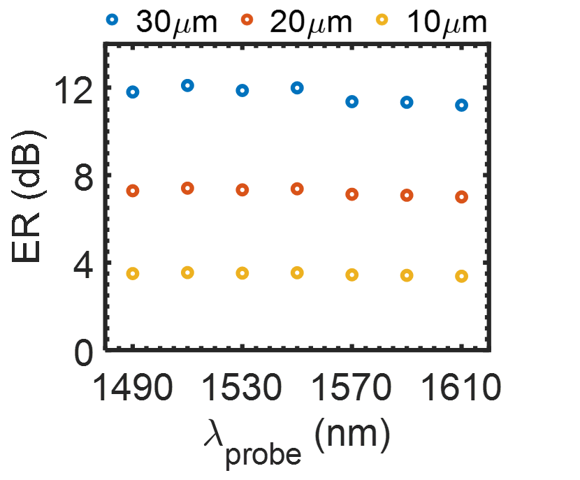
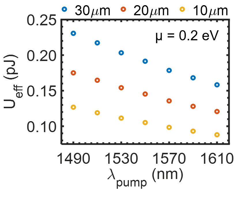
The broadband response of the device is studied by calculating the and at other wavelengths. Fig. 7a presents the as a function of the probe signal wavelength (), and Fig. 7b presents as a function of the pump signal wavelength () for eV. It is observed that the does not vary much in the studied wavelength range, which is expected because the variations of and in this range are minimal, as was shown in Fig. 2b. Unlike the , exhibits a relatively strong dependence on , where it is higher at shorter wavelengths. This agrees with experimental observations [45, 49], where it has been reported that a lower pump intensity is required to saturate graphene at longer pump wavelengths. This can be explained by the unique conical dispersion of graphene, which increases and widens at higher chemical potentials. Therefore, a pump signal with a higher energy would be required at short wavelengths to satisfy the Pauli-blocking condition, which is given by , as was explained in section III. values at other modulator lengths and chemical potentials are presented in supplementary section S3.
VI Modulation Performance
The device performance is determined by the electron heating and cooling dynamics in graphene [14, 40]. Graphene has a unique conical dispersion, where its density of states fades away at the Dirac point. Consequently, electrons in the vicinity of the Dirac point have a relatively low heat capacity. Upon photoexcitation, these electrons immediately scatter with one another, creating an ephemeral Fermi-Dirac distribution of hot thermalized electrons within a few tens to 150 femtoseconds [16, 17, 18]. Hence, photon energy is converted to electron heat. Eventually, hot electrons cool down in a few picoseconds by emitting optical and acoustic phonons, coupling with surface optical phonons, and most importantly through disorder-assisted scattering which dominates at room temperature [50, 51, 52, 53]. Thus, electrons first heat up through intraband electron-electron scattering, then they cool down through phonon- and disorder-assisted scattering. In addition, fewer layer graphene is characterized by faster electron heating and cooling dynamics [44, 14, 54].
In [32], a high-responsivity graphene-on-silicon slot waveguide photodetector has been demonstrated. Nonetheless, the performance of this device was limited by its µs rise time, which would correspond to a 7 KHz electrical bandwidth based on , where is the electrical bandwidth, and is the rise time [55]. In the literature, waveguide-integrated graphene photodetectors have been demonstrated with a bandwidth exceeding 110 GHz [56, 57, 58]. The relatively low bandwidth of the aforementioned graphene-on-silicon slot waveguide photodetector was attributed to the slow carrier heating and cooling dynamics in suspended graphene, where substrate-induced disorder-assisted scattering is absent. In another work [59], a graphene-on-silicon slot waveguide photodetector has been demonstrated, but with a 10 nm hBN layer placed beneath the graphene sheet. The reported bandwidth for this device was 65 GHz, even though its structure is not much different from the one reported in [32]. Graphene is not suspended when it forms a Van der Waals (vdW) heterostrcuture with hBN. The electron cooling dynamics in graphene–hBN vdW heterostructures are dominated by hot electron coupling to hyperbolic phonon polaritons (HPhPs), not disorder-assisted scattering [17, 25, 26, 27]. Experimentally, graphene on hBN demonstrated faster electron cooling dynamics than graphene on Si/SiO2 substrates [25, 28]. Therefore, the cooling pathway introduced by HPhPs is more efficient than disorder-assisted scattering, which could explain the enhanced bandwidth of the device reported in [59].

| Reference | /m | /m | |||||
|---|---|---|---|---|---|---|---|
| [12] | 19 dB | 3.5 dB | 4 µm | 0.875 dB/µm | 4.75 dB/µm | 260 fs | 35 fJ |
| [13] | n/a | 2.1 dB | 10 µm | 0.21 dB/µm | n/a | n/a | n/a a |
| [60] | negligible | 2.75 dB | 100 µm | 0.0275 dB/µm | negligible | n/a | n/a b |
| [61] | negligible | 1.1 dB c | 30 µm | 0.0367 dB/µm | negligible | 1.2 ps d | 1.38 pJ e |
| [62] | dB f | 11 dB | 288 µm g | 0.038 dB/µm | 0.0035 dB/µm | 1.29 µs | n/a h |
| This work | dB | 7.3 dB | 20 µm | 0.365 dB/µm | dB/µm | ¡600 fs | fJ |
a Maximum input light power is 46 mW; b Input light power is 60 mW; c Modulation depth is 22.7%; d Limited by the resolution time of the asynchronous pump–probe system; e Saturation threshold; f Waveguide loss before transferring graphene. g Length of the graphene coating on the waveguide. h 90– 109.6 mW switching power. n/a: not available (not reported).
An all-optical modulator that is based on graphene-on-silicon slot waveguides has not yet been demonstrated, to the best of our knowledge. As such, the electron heating and cooling dynamics and the corresponding response times of these devices are not reported in the literature. To ensure that our device performs ultrafast modulation and does not suffer from inefficient electron heating and cooling dynamics, hBN is sandwiched between the two graphene layers. In this heterostructure, the electron heat transfer channel is out-of-plane [25], which means that the sandwiched hBN layer provides a cooling pathway for both the upper and the lower graphene layers.
In order to calculate the recovery time of the switch, the electrical conductivity of graphene is first calculated using the following relation [63, 64]:
| (9) |
where is Planck’s constant. is the minimum conductivity taken from [63], and meV (K) is a typical width of the charge neutrality region for graphene on a BN substrate [65]. is a fitting parameter that accounts for disorder in graphene, and it determines the mobility and the slope of the conductivity curve. Higher disorder is manifested in the form of a wider charge neutrality region in the conductivity plot [52, 17]. By fitting the conductivity curve using Eq. 9, it is possible to model graphene with different carrier mobilities. The electron cooling time is taken as the electron relaxation time. For the case of graphene-on-hBN, it can be calculated from using the following relation [66]:
| (10) |
where is the electron charge, is the density of states of graphene, and is the total degeneracy due to the spin
degeneracy and the valley degeneracy [39]. Fig. 8 presents the calculated as a function of , which is found out to be fs within the range of 0.1– 0.2 eV, where is related to the carrier density () by [39]. This result is similar to the experimentally reported electron cooling times for graphene-on-hBN, which were in the range of 200– 400 fs in [28]. The switching time of the device is on the order of the electron heating time (fs) [16, 17, 18], because this is the time in which a sea of hot electrons is induced following a pump excitation; these electrons fill up the conduction band states leading to Pauli-blocking [67]. Then, the modulator reverts to its steady-state in a timescale of , which is fs in the case that is considered in Fig. 8. Based on these values, this device can theoretically operate as an all-optical modulator with a bandwidth in the hundreds of GHz [40]. The heating and cooling dynamics of additional graphene-hBN layers are expected to be similar to the case of double layer graphene, because each graphene layer forms a vdW heterostructure with hBN.
The pump fluence affects the carrier cooling time. In [28], pump-probe spectroscopy of graphene-hBN heterostructures was performed with pump fluences of 80, 60, and 50, for which the extracted carrier cooling times were 375 fs, 250 fs, and 200 fs (fs), respectively. These cooling times are similar to the electron cooling times that are presented in Fig. 8. Therefore, the energy of the pump signal does not need to be higher than , because the electron cooling time increases at higher pump fluences, which in turn decreases the switching performance of the device. The studied vdW heterostructure in [28], consisted of graphene on a hBN layer. In addition, it has been reported that the encapsulation of graphene in hBN induces ultrafast cooling pathways of hot electrons by HPhPs [26, 25]. It is possible to design high-performance all-optical modulators by building Gr/hBN heterostructures or by encapsulating graphene in hBN.
Table II presents the reported performance metrics of demonstrated on-chip all-optical graphene switches and modulators. The device that is presented in [12], is based on graphene-loaded plasmonic slot waveguides. It achieves the highest modulation efficiency (0.875 dB/µm) and the lowest switching energy (fJ), but is limited by an excessive . To meet the demands of next-generation telecom and datacom networks, photonic devices with an dB are required [8]. Nevertheless, this device has made a significant contribution in all-optical switching because it has demonstrated an unprecedented recovery time of 260 fs using graphene. The authors explained that this result could be because of the ultrafast carrier diffusion out of the 30 nm narrow slot region. To the best of our knowledge, a dedicated study of the influence of the graphene sheet area on the carrier relaxation time has not been reported in the literature. It is not inconceivable that the ultrafast recovery time of fs was brought about by the small graphene sheet area. In fact, pump-probe spectroscopy of waveguide-integrated germanium revealed that the lifetime of photoexcited carriers increases with the germanium length and width [68]. This could also be the case for waveguide-integrated graphene devices. Therefore, it might be possible to achieve ultrafast switching beyond a recovery time of fs, by building Gr/hBN all-optical modulators with a small device area; the smaller area enables faster carrier diffusion across the device, and the use of Gr/hBN heterostructures achieves ultrafast carrier cooling that is four times faster than that on a SiO2 substrate [28]. Therefore, further investigation of the influence of the graphene sheet area on the carrier cooling dynamics is required. In practice, however, the absorption of graphene is small, which necessitates the need for longer devices. The use of Gr/hBN heterostructures accelerates the carrier cooling dynamics of graphene, even for large area sheets. For instance, a 200 fs (fs) carrier cooling time at a pump fluence of J/cm2 was reported in [28], for a Gr/hBN heterostructure that is tens of micrometres long. The non-plasmonic devices that were reported in [60, 61, 62] have a much lower and can achieve high modulation efficiencies at large , but their switching energies may exceed pJ/bit at these lengths. Though this device is longer than other devices, it achieves a relatively high modulation efficiency (0.365 dB/µm), energy-efficient switching (fJ) and ultrafast recovery (fs) at an almost negligible of 0.45 dB.
The fabrication process of Si sot waveguides is presented in [32], where the waveguide pattern is defined on a commercial silicon-on-insulator (SOI) substrate using electron beam lithography (EBL). Optoelectronic devices with a Gr/hBN/Gr heterostructure were fabricated in [69]. This heterostructure is prepared by the dry transfer technique [70], where graphene and hBN layers are first separately exfoliated onto Si/SiO2 substrates, and each layer is then picked up by a polymer stamp. In [71], hBN was picked up by a single layer graphene that is attached to a PMMA membrane. By picking up an additional layer of graphene, a Gr/hBN/Gr heterostructure is formed. In [61], a waveguide-integrated all-optical graphene modulator with partially suspended graphene was demonstrated. There, a PMMA/Gr film was transferred onto the waveguides and patterned by EBL to control the modulation depth of the device. The redundant graphene layer was etched off by reactive ion etching (RIE) using oxygen. PMMA was removed by soaking the chip in acetone. By following a similar approach, a PMMA film with a Gr/hBN/Gr heterostructure could be transferred onto the Si slot waveguides, to build the double-graphene modulator that is shown in Fig. 1a.
The presence of surface defects in graphene, like wrinkles, induces a scattering loss, which increases the non-saturable fraction of the absorption () [44]. This in turn degrades the modulation efficiency, increases the switching energy, and contributes to a higher . Further advances in graphene transfer methods will contribute to the development of more efficient and reliable graphene-based devices.
VII Conclusion
We propose a novel design of a high-performance all-optical modulator that is based on graphene and hexagonal boron nitride (hBN) heterostructures, that are hybrid integrated into silicon slot waveguides. Simulations were performed to optimize the design, where an 8 µm long taper is introduced to achieve a 97% coupling efficiency between the slotted modulator waveguide and silicon strip waveguides. Moreover, the switching energy, modulation efficiency, broadband response, and modulation performance of the device were investigated. Using this device, a high extinction ratio (ER) of 7.3 dB, an ultra-low insertion loss (IL) of 0.6 dB, and energy-efficient switching (0.33 pJ/bit) are attainable for a 20 µm long modulator with double layer graphene. In addition, it performs ultrafast switching with a recovery time of fs, and could potentially be employed as a high-performance all-optical modulator with an ultra-high bandwidth in the hundreds of GHz. Furthermore, stacking additional layers of Gr/hBN heterostructures enhances the modulation efficiency of the device, while theoretically maintaining the same ultrafast response. The high-performance metrics of this device across a wide wavelength range are expected to serve the needs of next-generation optical computing systems.
Acknowledgment
Support from the NYUAD Center for Cyber Security research grant is gratefully acknowledged.
References
- [1] H. Chen, C. Wang, H. Ouyang, Y. Song, and T. Jiang, “All-optical modulation with 2D layered materials: status and prospects,” Nanophotonics, vol. 1, no. ahead-of-print, 2020.
- [2] V. Rutckaia and J. Schilling, “Ultrafast low-energy all-optical switching,” Nature Photonics, vol. 14, no. 1, pp. 4–6, 2020.
- [3] Z. Chai, X. Hu, F. Wang, X. Niu, J. Xie, and Q. Gong, “Ultrafast all-optical switching,” Advanced Optical Materials, vol. 5, no. 7, p. 1600665, 2017.
- [4] V. Sasikala and K. Chitra, “All optical switching and associated technologies: a review,” Journal of Optics, vol. 47, no. 3, pp. 307–317, 2018.
- [5] Neira, Andres D and Wurtz, Gregory A and Ginzburg, Pavel and Zayats, Anatoly V, “Ultrafast all-optical modulation with hyperbolic metamaterial integrated in Si photonic circuitry,” Optics express, vol. 22, no. 9, pp. 10 987–10 994, 2014.
- [6] B.-J. Huang, C.-T. Tsai, Y.-H. Lin, C.-H. Cheng, H.-Y. Wang, Y.-C. Chi, P.-H. Chang, C.-I. Wu, and G.-R. Lin, “Sigec waveguide for all-optical data switching,” ACS Photonics, vol. 5, no. 6, pp. 2251–2260, 2018.
- [7] Y. Li, A. Bhattacharyya, C. Thomidis, T. D. Moustakas, and R. Paiella, “Ultrafast all-optical switching with low saturation energy via intersubband transitions in gan/aln quantum-well waveguides,” Optics express, vol. 15, no. 26, pp. 17 922–17 927, 2007.
- [8] M. A. Giambra, V. Miseikis, S. Pezzini, S. Marconi, A. Montanaro, F. Fabbri, V. Sorianello, A. C. Ferrari, C. Coletti, and M. Romagnoli, “Wafer-scale integration of graphene-based photonic devices,” ACS nano, vol. 15, no. 2, pp. 3171–3187, 2021.
- [9] K. Nozaki, T. Tanabe, A. Shinya, S. Matsuo, T. Sato, H. Taniyama, and M. Notomi, “Sub-femtojoule all-optical switching using a photonic-crystal nanocavity,” Nature Photonics, vol. 4, no. 7, pp. 477–483, 2010.
- [10] C. Husko, A. De Rossi, S. Combrié, Q. V. Tran, F. Raineri, and C. W. Wong, “Ultrafast all-optical modulation in GaAs photonic crystal cavities,” Applied Physics Letters, vol. 94, no. 2, p. 021111, 2009.
- [11] M. Takiguchi, N. Takemura, K. Tateno, K. Nozaki, S. Sasaki, S. Sergent, E. Kuramochi, T. Wasawo, A. Yokoo, A. Shinya, et al., “All-Optical InAsP/InP Nanowire Switches Integrated in a Si Photonic Crystal,” ACS Photonics, vol. 7, no. 4, pp. 1016–1021, 2020.
- [12] M. Ono, M. Hata, M. Tsunekawa, K. Nozaki, H. Sumikura, H. Chiba, and M. Notomi, “Ultrafast and energy-efficient all-optical switching with graphene-loaded deep-subwavelength plasmonic waveguides,” Nature Photonics, vol. 14, no. 1, pp. 37–43, 2020.
- [13] F. Sun, L. Xia, C. Nie, C. Qiu, L. Tang, J. Shen, T. Sun, L. Yu, P. Wu, S. Yin, et al., “An all-optical modulator based on a graphene–plasmonic slot waveguide at 1550 nm,” Applied Physics Express, vol. 12, no. 4, p. 042009, 2019.
- [14] M. AlAloul and M. Rasras, “Low insertion loss plasmon-enhanced graphene all-optical modulator,” ACS Omega, 2021.
- [15] S. A. Maier, Plasmonics: fundamentals and applications. Springer Science & Business Media, 2007.
- [16] K.-J. Tielrooij, L. Piatkowski, M. Massicotte, A. Woessner, Q. Ma, Y. Lee, K. S. Myhro, C. N. Lau, P. Jarillo-Herrero, N. F. van Hulst, et al., “Generation of photovoltage in graphene on a femtosecond timescale through efficient carrier heating,” Nature nanotechnology, vol. 10, no. 5, pp. 437–443, 2015.
- [17] M. Alaloul and M. Rasras, “Plasmon-enhanced graphene photodetector with cmos-compatible titanium nitride,” JOSA B, vol. 38, no. 2, pp. 602–610, 2021.
- [18] Y. Chen, Y. Li, Y. Zhao, H. Zhou, and H. Zhu, “Highly efficient hot electron harvesting from graphene before electron-hole thermalization,” Science advances, vol. 5, no. 11, p. eaax9958, 2019.
- [19] X. Gan, R.-J. Shiue, Y. Gao, I. Meric, T. F. Heinz, K. Shepard, J. Hone, S. Assefa, and D. Englund, “Chip-integrated ultrafast graphene photodetector with high responsivity,” Nature photonics, vol. 7, no. 11, pp. 883–887, 2013.
- [20] N. Youngblood, Y. Anugrah, R. Ma, S. J. Koester, and M. Li, “Multifunctional graphene optical modulator and photodetector integrated on silicon waveguides,” Nano letters, vol. 14, no. 5, pp. 2741–2746, 2014.
- [21] C. T. Phare, Y.-H. D. Lee, J. Cardenas, and M. Lipson, “Graphene electro-optic modulator with 30 GHz bandwidth,” Nature Photonics, vol. 9, no. 8, pp. 511–514, 2015.
- [22] A. Pospischil, M. Humer, M. M. Furchi, D. Bachmann, R. Guider, T. Fromherz, and T. Mueller, “Cmos-compatible graphene photodetector covering all optical communication bands,” Nature Photonics, vol. 7, no. 11, pp. 892–896, 2013.
- [23] D. Akinwande, C. Huyghebaert, C.-H. Wang, M. I. Serna, S. Goossens, L.-J. Li, H.-S. P. Wong, and F. H. Koppens, “Graphene and two-dimensional materials for silicon technology,” Nature, vol. 573, no. 7775, pp. 507–518, 2019.
- [24] J. Jiang, J. H. Chu, and K. Banerjee, “Cmos-compatible doped-multilayer-graphene interconnects for next-generation vlsi,” in 2018 IEEE International Electron Devices Meeting (IEDM). IEEE, 2018, pp. 34–5.
- [25] K.-J. Tielrooij, N. C. Hesp, A. Principi, M. B. Lundeberg, E. A. Pogna, L. Banszerus, Z. Mics, M. Massicotte, P. Schmidt, D. Davydovskaya, et al., “Out-of-plane heat transfer in van der Waals stacks through electron–hyperbolic phonon coupling,” Nature nanotechnology, vol. 13, no. 1, pp. 41–46, 2018.
- [26] A. Principi, M. B. Lundeberg, N. C. Hesp, K.-J. Tielrooij, F. H. Koppens, and M. Polini, “Super-Planckian electron cooling in a van der Waals stack,” Physical review letters, vol. 118, no. 12, p. 126804, 2017.
- [27] P. Huang, E. Riccardi, S. Messelot, H. Graef, F. Valmorra, J. Tignon, T. Taniguchi, K. Watanabe, S. Dhillon, B. Placais, et al., “Ultra-long carrier lifetime in neutral graphene-hBN van der Waals heterostructures under mid-infrared illumination,” Nature communications, vol. 11, no. 1, pp. 1–9, 2020.
- [28] D. Golla, A. Brasington, B. J. LeRoy, and A. Sandhu, “Ultrafast relaxation of hot phonons in graphene-hBN heterostructures,” APL Materials, vol. 5, no. 5, p. 056101, 2017.
- [29] W. Gannett, W. Regan, K. Watanabe, T. Taniguchi, M. Crommie, and A. Zettl, “Boron nitride substrates for high mobility chemical vapor deposited graphene,” Applied Physics Letters, vol. 98, no. 24, p. 242105, 2011.
- [30] C. R. Dean, A. F. Young, I. Meric, C. Lee, L. Wang, S. Sorgenfrei, K. Watanabe, T. Taniguchi, P. Kim, K. L. Shepard, et al., “Boron nitride substrates for high-quality graphene electronics,” Nature nanotechnology, vol. 5, no. 10, pp. 722–726, 2010.
- [31] P. Zomer, S. Dash, N. Tombros, and B. Van Wees, “A transfer technique for high mobility graphene devices on commercially available hexagonal boron nitride,” Applied Physics Letters, vol. 99, no. 23, p. 232104, 2011.
- [32] J. Wang, Z. Cheng, Z. Chen, X. Wan, B. Zhu, H. K. Tsang, C. Shu, and J. Xu, “High-responsivity graphene-on-silicon slot waveguide photodetectors,” Nanoscale, vol. 8, no. 27, pp. 13 206–13 211, 2016.
- [33] Z. Cheng, J. Wang, B. Zhu, K. Xu, W. Zhou, H. K. Tsang, and C. Shu, “Graphene absorption enhancement using silicon slot waveguides,” in 2015 IEEE Photonics Conference (IPC). IEEE, 2015, pp. 186–187.
- [34] J. Wang, Z. Cheng, H. K. Tsang, and C. Shu, “In-plane saturable absorption of graphene on a silicon slot waveguide,” in 2016 21st OptoElectronics and Communications Conference (OECC) held jointly with 2016 International Conference on Photonics in Switching (PS). IEEE, 2016, pp. 1–3.
- [35] Z. Wang, N. Zhu, Y. Tang, L. Wosinski, D. Dai, and S. He, “Ultracompact low-loss coupler between strip and slot waveguides,” Optics letters, vol. 34, no. 10, pp. 1498–1500, 2009.
- [36] C. Elias, P. Valvin, T. Pelini, A. Summerfield, C. Mellor, T. Cheng, L. Eaves, C. Foxon, P. Beton, S. Novikov, et al., “Direct band-gap crossover in epitaxial monolayer boron nitride,” Nature communications, vol. 10, no. 1, pp. 1–7, 2019.
- [37] S. Serna, W. Zhang, X. Leroux, D. Gao, D. Zhang, L. Vivien, and E. Cassan, “Potential for large optical gain improvement of erbium-doped slot waveguide amplifiers in silicon photonics,” JOSA B, vol. 31, no. 9, pp. 2021–2028, 2014.
- [38] G. Deokar, J. Avila, I. Razado-Colambo, J.-L. Codron, C. Boyaval, E. Galopin, M.-C. Asensio, and D. Vignaud, “Towards high quality cvd graphene growth and transfer,” Carbon, vol. 89, pp. 82–92, 2015.
- [39] J.-M. Liu and I.-T. Lin, Graphene photonics. Cambridge University Press, 2018.
- [40] W. Li, B. Chen, C. Meng, W. Fang, Y. Xiao, X. Li, Z. Hu, Y. Xu, L. Tong, H. Wang, et al., “Ultrafast all-optical graphene modulator,” Nano letters, vol. 14, no. 2, pp. 955–959, 2014.
- [41] J.-H. Chen, B.-C. Zheng, G.-H. Shao, S.-J. Ge, F. Xu, and Y.-Q. Lu, “An all-optical modulator based on a stereo graphene–microfiber structure,” Light: Science & Applications, vol. 4, no. 12, pp. e360–e360, 2015.
- [42] Y. Liao, G. Feng, H. Zhou, J. Mo, H. Sun, and S. Zhou, “Ultra-broadband all-optical graphene modulator,” IEEE Photonics Technology Letters, vol. 30, no. 8, pp. 661–664, 2018.
- [43] Q. Bao, H. Zhang, Y. Wang, Z. Ni, Y. Yan, Z. X. Shen, K. P. Loh, and D. Y. Tang, “Atomic-layer graphene as a saturable absorber for ultrafast pulsed lasers,” Advanced Functional Materials, vol. 19, no. 19, pp. 3077–3083, 2009.
- [44] Q. Bao, H. Zhang, Z. Ni, Y. Wang, L. Polavarapu, Z. Shen, Q.-H. Xu, D. Tang, and K. P. Loh, “Monolayer graphene as a saturable absorber in a mode-locked laser,” Nano Research, vol. 4, no. 3, pp. 297–307, 2011.
- [45] F. Zhang, S. Han, Y. Liu, Z. Wang, and X. Xu, “Dependence of the saturable absorption of graphene upon excitation photon energy,” Applied Physics Letters, vol. 106, no. 9, p. 091102, 2015.
- [46] K. J. Ooi, P. C. Leong, L. K. Ang, and D. T. Tan, “All-optical control on a graphene-on-silicon waveguide modulator,” Scientific reports, vol. 7, no. 1, pp. 1–9, 2017.
- [47] H. E. Romero, N. Shen, P. Joshi, H. R. Gutierrez, S. A. Tadigadapa, J. O. Sofo, and P. C. Eklund, “n-type behavior of graphene supported on Si/SiO2 substrates,” Acs Nano, vol. 2, no. 10, pp. 2037–2044, 2008.
- [48] A. Fong, R. Coackley, J. J. Dupre, S. J. Greer, S. Linkwitz, J. R. Page, R. E. Pratt, D. K. Rytting, G. D. Sasaki, and G. D. Sasaki, “12 - measurements and analysis,” in Reference Data for Engineers (Ninth Edition), W. M. Middleton and M. E. Van Valkenburg, Eds. Woburn: Newnes, 2002, pp. 12–1 – 12–39. [Online]. Available: http://www.sciencedirect.com/science/article/pii/B9780750672917500145
- [49] G. Demetriou, H. T. Bookey, F. Biancalana, E. Abraham, Y. Wang, W. Ji, and A. K. Kar, “Nonlinear optical properties of multilayer graphene in the infrared,” Optics express, vol. 24, no. 12, pp. 13 033–13 043, 2016.
- [50] J. C. Song, M. Y. Reizer, and L. S. Levitov, “Disorder-assisted electron-phonon scattering and cooling pathways in graphene,” Physical review letters, vol. 109, no. 10, p. 106602, 2012.
- [51] Q. Ma, N. M. Gabor, T. I. Andersen, N. L. Nair, K. Watanabe, T. Taniguchi, and P. Jarillo-Herrero, “Competing channels for hot-electron cooling in graphene,” Physical review letters, vol. 112, no. 24, p. 247401, 2014.
- [52] J.-H. Chen, C. Jang, S. Adam, M. Fuhrer, E. D. Williams, and M. Ishigami, “Charged-impurity scattering in graphene,” Nature physics, vol. 4, no. 5, pp. 377–381, 2008.
- [53] M. W. Graham, S.-F. Shi, D. C. Ralph, J. Park, and P. L. McEuen, “Photocurrent measurements of supercollision cooling in graphene,” Nature Physics, vol. 9, no. 2, pp. 103–108, 2013.
- [54] R. W. Newson, J. Dean, B. Schmidt, and H. M. van Driel, “Ultrafast carrier kinetics in exfoliated graphene and thin graphite films,” Optics Express, vol. 17, no. 4, pp. 2326–2333, 2009.
- [55] G. D. Brown, “Bandwidth and rise time calculations for digital multimode fiber-optic data links,” Journal of Lightwave Technology, vol. 10, no. 5, pp. 672–678, 1992.
- [56] Y. Ding, Z. Cheng, X. Zhu, K. Yvind, J. Dong, M. Galili, H. Hu, N. A. Mortensen, S. Xiao, and L. K. Oxenløwe, “Ultra-compact integrated graphene plasmonic photodetector with bandwidth above 110 ghz,” Nanophotonics, vol. 9, no. 2, pp. 317–325, 2020.
- [57] D. Schall, E. Pallecchi, G. Ducournau, V. Avramovic, M. Otto, and D. Neumaier, “Record high bandwidth integrated graphene photodetectors for communication beyond 180 gb/s,” in Optical Fiber Communication Conference. Optical Society of America, 2018, pp. M2I–4.
- [58] P. Ma, Y. Salamin, B. Baeuerle, A. Josten, W. Heni, A. Emboras, and J. Leuthold, “Plasmonically enhanced graphene photodetector featuring 100 gbit/s data reception, high responsivity, and compact size,” ACS Photonics, vol. 6, no. 1, pp. 154–161, 2018.
- [59] S. Schuler, D. Schall, D. Neumaier, L. Dobusch, O. Bethge, B. Schwarz, M. Krall, and T. Mueller, “Controlled generation of ap–n junction in a waveguide integrated graphene photodetector,” Nano letters, vol. 16, no. 11, pp. 7107–7112, 2016.
- [60] F. Sun, L. Xia, C. Nie, J. Shen, Y. Zou, G. Cheng, H. Wu, Y. Zhang, D. Wei, S. Yin, et al., “The all-optical modulator in dielectric-loaded waveguide with graphene-silicon heterojunction structure,” Nanotechnology, vol. 29, no. 13, p. 135201, 2018.
- [61] H. Wang, N. Yang, L. Chang, C. Zhou, S. Li, M. Deng, Z. Li, Q. Liu, C. Zhang, Z. Li, et al., “CMOS-compatible all-optical modulator based on the saturable absorption of graphene,” Photonics Research, vol. 8, no. 4, pp. 468–474, 2020.
- [62] C. Qiu, C. Zhang, H. Zeng, and T. Guo, “High-performance graphene-on-silicon nitride all-optical switch based on a mach–zehnder interferometer,” Journal of Lightwave Technology, vol. 39, no. 7, pp. 2099–2105, 2021.
- [63] Y. Lin, Q. Ma, P.-C. Shen, B. Ilyas, Y. Bie, A. Liao, E. Ergeçen, B. Han, N. Mao, X. Zhang, et al., “Asymmetric hot-carrier thermalization and broadband photoresponse in graphene-2D semiconductor lateral heterojunctions,” Science advances, vol. 5, no. 6, p. eaav1493, 2019.
- [64] M. Alaloul and J. B. Khurgin, “Plasmonic photovoltaic double-graphene detector integrated into tin slot waveguides,” IEEE Photonics Journal, vol. 13, no. 6, pp. 1–8, 2021.
- [65] J. C. Song, M. S. Rudner, C. M. Marcus, and L. S. Levitov, “Hot carrier transport and photocurrent response in graphene,” Nano letters, vol. 11, no. 11, pp. 4688–4692, 2011.
- [66] L. Hamidouche, A. Montanaro, M. Rosticher, E. Grimaldi, B. Poupet, T. Taniguchi, K. Watanabe, B. Placais, E. Baudin, and P. Legagneux, “Optoelectronic mixing in high-mobility graphene,” ACS Photonics, 2020.
- [67] M. Alaloul and J. B. Khurgin, “Electrical control of all-optical graphene switches,” Optics Express, vol. 30, no. 2, pp. 1950–1966, 2022.
- [68] S. A. Srinivasan, M. Pantouvaki, P. Verheyen, G. Lepage, P. Absil, J. Van Campenhout, and D. Van Thourhout, “Extraction of carrier lifetime in ge waveguides using pump probe spectroscopy,” Applied Physics Letters, vol. 108, no. 21, p. 211101, 2016.
- [69] S.-B. Song, S. Yoon, S. Y. Kim, S. Yang, S.-Y. Seo, S. Cha, H.-W. Jeong, K. Watanabe, T. Taniguchi, G.-H. Lee, et al., “Deep-ultraviolet electroluminescence and photocurrent generation in graphene/hbn/graphene heterostructures,” Nature communications, vol. 12, no. 1, pp. 1–9, 2021.
- [70] L. Wang, I. Meric, P. Huang, Q. Gao, Y. Gao, H. Tran, T. Taniguchi, K. Watanabe, L. Campos, D. Muller, et al., “One-dimensional electrical contact to a two-dimensional material,” Science, vol. 342, no. 6158, pp. 614–617, 2013.
- [71] G. Argentero, A. Mittelberger, M. Reza Ahmadpour Monazam, Y. Cao, T. J. Pennycook, C. Mangler, C. Kramberger, J. Kotakoski, A. Geim, and J. C. Meyer, “Unraveling the 3d atomic structure of a suspended graphene/hbn van der waals heterostructure,” Nano letters, vol. 17, no. 3, pp. 1409–1416, 2017.