Casimir-Polder interactions of Rydberg atoms
with graphene-based van der Waals heterostructures
Abstract
We investigate the thermal Casimir-Polder (CP) potential of 87Rb atoms in Rydberg S-states near single- and double-layer graphene. The dependence of the CP potential on parameters such as atom-surface distance, temperature, principal quantum number and graphene Fermi energy are explored. Through large scale numerical simulations, we show that, in the non-retarded regime, the CP potential is dominated by the non-resonant and evanescent-wave terms which are monotonic, and that, in the retarded regime, the CP potential exhibits spatial oscillations. We identify that the most important contributions to the resonant component of the CP potential come from the S-P and S-P transitions. Scaling of the CP potential as a function of the principal quantum number and temperature is obtained. A heterostructure comprising hexagonal boron nitride layers sandwiched between two graphene layers is also studied. When the boron nitride layer is sufficiently thin, the CP potential can be weakened by changing the Fermi energy of the top graphene layer. Our study provides insights for understanding and controlling CP potentials experienced by Rydberg atoms near single and multi-layer graphene-based van der Waals heterostructures.
I Introduction
The development of ultracold-atom physics as platforms for chip-based matter wave manipulation Chen and Fan 2020, high-accuracy time keeping systems Liu et al. 2018; Ren et al. 2020, quantum computing and simulation Knight and Walmsley 2019; Acín et al. 2018; Meinert et al. 2020; Geier et al. 2021 is an active research field. Understanding atom-surface interactions is essential for achieving near-surface atom trapping, as required for the operation of micro-fabricated atom chips. There is a substantial body of research on trapping ground-state atoms in metallic-wire-based atom chips Haug et al. 2019; Scheel et al. 2005; Rekdal et al. 2004; Folman et al. 2002; Henkel et al. 1999; Hinds and Hughes 1999; Jones et al. 2003 as well as on the interactions of ground-state atoms with various structures of metallic and perfect conductors Messina and Passante 2007; Vasile and Passante 2008; Ferreri et al. 2019.
A conclusive review of atom-surface physics can be found in Laliotis et al. 2021a.
It is known that metallic-wire-based atom chips generate spatially rough trapping potential due to imperfections in the wires Sinuco-León et al. 2011; Sinuco-León et al. 2018; Aigner et al. 2008; Japha et al. 2008; Schumm et al. 2005, high Johnson-noise currents and strong Casimir-Polder (CP) attractive interactions between the atoms and the chip, causing, for example, tunnelling losses Henkel et al. 2003; Lin et al. 2004; Laliotis et al. 2021b. In order to enhance the functionality of such atom chips, different materials are needed for the current-carrying wires. Recent studies have shown that two-dimensional (2D) materials could offer desirable properties for overcoming the limitations of using metallic conductors as current-carrying wires Sinuco-León et al. 2018; Wongcharoenbhorn et al. 2021.
There is also enduring interest in the technological applications of two-dimensional (2D) materials, including graphene, for display devices Ergoktas et al. 2021, flexible sensors Liu et al. 2020a; Kim et al. 2020; Carvalho et al. 2021, photo detectors Mišeikis et al. 2020; Gosciniak et al. 2020; Gosciniak and Khurgin 2020; Zhu et al. 2021; AlAloul and Rasras 2021, vertical field-effect transistors Britnell et al. 2013; Liu et al. 2020b, and atom chips Wongcharoenbhorn et al. 2021. New properties and methods of cooling or patterning 2D materials have been studied Ribeiro and Terças 2016; Candussio et al. 2021; Tripathi et al. 2021; Ta et al. 2020; Wei et al. 2021; Cui et al. 2021a; Liu et al. 2021a; Slizovskiy et al. 2021; Greenaway et al. 2021. As current-carrying wires in atom chips, graphene has desirable electronic properties: it has a very low density of electronic states, high carrier mobility and a linear band structure with zero band gap in the vicinity of the Dirac points McCann 2012, which leads to Johnson noise and CP attraction far below those typically found for metallic conductors on bulk substrates Sinuco-León et al. 2011; Fermani et al. 2007; Sinuco-León et al. 2018; Wongcharoenbhorn et al. 2021.
Importantly, smooth trapping potentials can be obtained using graphene. For example,
graphene made from a helium-ion beam lithography technique
has edge roughness of order Aigner et al. 2008, while the surface roughness of graphene encapsulated in hexagonal boron nitride (hBN) is on the order of Thomsen et al. 2017.
The coupling of atoms with graphene’s surface plasmons might be tuneable via changing the Fermi energy of graphene as the plasmon frequency is proportional to the fourth root of its electronic density Ju et al. 2011; Yan et al. 2013; Cui et al. 2021b; Haakh et al. 2014; Zeng and Zubairy 2021. Previous studies have shown that this could be used to tailor the CP interactions of atoms trapped near graphene Cysne et al. 2014; Liu et al. 2021b; Henkel et al. 2018; Chaichian et al. 2012; Churkin et al. 2010; Bordag et al. 2006; Cysne et al. 2016; Nichols et al. 2016; Klimchitskaya and Mostepanenko 2020; Kaur et al. 2014; Khusnutdinov et al. 2018.

In recent years, the study of interactions between Rydberg atoms and surfaces has attracted much attention. Such studies could help us understand the atom-surface interaction for highly excited atomic states, and open new quantum technological applications Šibalić and Adams 2018, for example by integrating Rydberg atoms with condensed matter quantum materials like graphene. Rydberg atoms are highly excited atoms with large principal quantum number, i.e. . The size of Rydberg atoms is proportional to , and can be a micron when , resulting in weakly bound valence electrons and high electric polarizability, which in turn causes strong interactions with nearby surfaces Kohlhoff 2016. The lifetime associated with spontaneous emission, i.e. at , is proportional to . The long lifetime of Rydberg states allows us to exploit Rydberg atoms for quantum computing and simulation Hermann-Avigliano et al. 2014; Wu et al. 2021. Atomic transition frequencies between adjacent Rydberg states are typically in the microwave-terahertz regions, which are in the same window as thermal energies at room temperature; Rydberg atoms interact resonantly with thermal photons, leading to enhanced CP interactions compared to ground-state atoms Ellingsen et al. 2010. Strong coupling between Rydberg atoms and surface plasmon polaritons or surface phonon polaritons have also been studied both experimentally and theoretically Törmä and Barnes 2014; Kübler et al. 2013; Ribeiro et al. 2013; Sheng et al. 2016.
There have been previous studies of the CP interactions of excited two-level or realistic Rydberg atoms near mirrors, metallic and dielectric surfaces, and metamaterials Barton 1974; Power and Thirunamachandran 1982; Barton 1988; Meschede et al. 1990; Hinds and Sandoghdar 1991; Bambini and Robinson 1992; Fichet et al. 1995; Gorza et al. 2001; Bushev et al. 2004; Buhmann et al. 2004; Gorza and Ducloy 2006; Buhmann and Welsch 2008; Schiefele and Henkel 2010; Crosse et al. 2010; Antezza et al. 2014; Ribeiro et al. 2015; Armata et al. 2016; Carvalho et al. 2018; Yang et al. 2019; Fang et al. 2019; Buhmann et al. 2021, as well as investigations of the CP interactions of a laser-driven atom and a surface Fuchs et al. 2018. The CP interactions between excited molecules or ions and metallic or dielectric bodies have also been studied Wilson et al. 2003; Bushev et al. 2004; Barcellona et al. 2016. However, CP interactions between Rydberg atoms and 2D nano-structures such as graphene have not been fully explored. To the best of our knowledge, the Rydberg atom-graphene interaction has only been studied in Ref. Ribeiro and Scheel 2013, which focuses on the zero-temperature limit and shows that graphene can shield the CP force emanating from a metallic substrate when graphene-substrate distances are larger than m.
Integrating Rydberg atoms with graphene could lead to promising and novel quantum devices M. et al. 2011; Wade et al. 2016; Saffman 2016.
In this work, we focus on investigating the CP interactions of a 87Rb atom in Rydberg S states with graphene. Two notable features, which are not found in ground-state atoms in the zero-temperature limit, emerge: stimulated atomic transitions due to thermal photons give rise to resonant interactions, which can be further distinguished into attractive and repulsive potentials, and the large sizes of Rydberg atoms give rise to quadrupole interactions at short atom-surface distances.
The paper is organized as follows. In Sec. II, we provide the quantum field theoretical description of the CP potential for atoms in Rydberg states and a brief description of Rydberg atoms. In Sec. III, we first compare the CP potential of a 87Rb atom in Rydberg states near a suspended single layer of graphene whose conductivity is described by the Kubo model, and a -m-thick gold sheet whose optical properties are described by the Drude model. We also consider another model of graphene, with the results presented, which includes non-local effects such as lattice defects. In Sec. IV, we present detailed calculations of the CP potential of single-layer graphene, which allow us to see various characteristics of Rydberg atoms near graphene that are different from those of ground-state atoms, especially effects arising from resonant interactions. In Sec. V, we find simple fitted empirical functions, which capture the scaling of the CP potential with principal quantum number and the temperature dependence of the interaction. Finally, in Sec. VI, we extend our study into graphene-based van der Waals heterostructures comprising two layers of graphene separated by air or hexagonal boron-nitride (hBN). This allows us to change the spacing between the graphene layers and change their chemical potentials in order to tune the interactions between the trapped atoms and the heterostructures. We conclude in Sec. VII.
II Casimir-Polder Potential near Planar Structures
In this section, we will present a theoretical description of the CP energy shift of highly excited Rydberg atoms near planar layered structures. Considering only ultracold atoms in Bose-Einstein condensates allows us to disregard the velocity-dependent CP potential since the atoms are not moving at a relativistic speed Scheel and Buhmann 2009. Further details of the formalism used can be found in, for example, Refs. Crosse et al. 2010; Scheel and Buhmann 2008; Buhmann 2012; Buhmann and Scheel 2008. The CP potential arises from the coupling between an atom and the surrounding body-modified electromagnetic radiation, described by the coupling Hamiltonian . The interaction Hamiltonian in the case of a Rydberg atom can be split into dipole interactions (first term) and quadrupole interactions (second term):
| (1) |
where and are the atomic dipole moment and quadrupole moment operators, respectively, with being the electromagnetic field at the position of the atom, , denotes the Frobenius inner product and tensor product. The energy-level shift up to the second order, for an atom in state and the body-modified electromagnetic field in state , is Crosse et al. 2010
| (2) |
where are the unperturbed energy eigenvalues of the atom-field system: and are the quantum numbers of the Rydberg state and the photon field, respectively. This energy shift can be expressed in terms of the Green’s tensor, which can be decomposed into bulk and scattering parts. It follows that the energy shift can be split into two components: the position-independent self-energy (associated with the bulk part of the Green’s tensor) similar to the Lamb shift and the position-dependent component (associated with the scattering part of the Green’s tensor), which is, namely, the CP potential.
For an atom, at position in the planar system shown in Fig. 1, in an incoherent superposition of internal-energy eigenstates (specified by the principal quantum number , the orbital angular momentum quantum number , the total angular momentum quantum number , and the -component of the total angular momentum quantum number ) with probabilities as described by a density matrix
| (3) |
the total thermal CP potential at environment temperature can be written as Scheel and Buhmann 2008; Buhmann and Scheel 2008
| (4) |
Here, is the position-dependent part of , is the non-resonant potential due to virtual photons and is the resonant potential due to real thermal photons.
For the potentials due to dipole interactions, the non-resonant term is given by Buhmann 2012
| (5) |
whereas, the resonant term is given by
| (6) |
where is the permeability of free space, the Boltzmann constant, is the scattering Green’s tensor (see Appendix A for details), and is the dipole matrix element. The atomic dipole polarizability as a function of radiation frequency, , is defined as
| (7) |
with denoting the atomic transition angular frequencies. The purely imaginary frequencies , are the Matsubara frequencies and is the average thermal photon number in accordance with Bose-Einstein statistics. Following the separation of the scattering Green’s tensor into propagating-wave and evanescent-wave components, the resonant term of the CP potential can also be split into two components as well.
In our calculations, the binding energy of the Rydberg series is given by Gallagher 1988, where is the Rydberg energy and . Here, is the quantum defect Seaton 1983 whose values for 87Rb are tabulated in Table 1.
The electron wavefunction at position with respect to the ion core, , for the valence electron is described by the Schrödinger equation
| (8) |
where is the electronic charge, is the reduced mass with being the mass of the atom, is the electronic mass, and is a model potential as given in Ref. Robertson et al. 2021, which accounts for the finite size of the core at short range. Eq. (8) can be separated into angular and radial equations which yield, in standard notation, spherical harmonics and radial wavefunctions as solutions, respectively. In this work, the radial wavefunctions are calculated numerically using the tool provided in Ref. Robertson et al. 2021 through Numerov’s method Numerov 1927.
| State | ||
|---|---|---|
| 3.1311804 | 0.1784 | |
| 2.6548849 | 0.2900 | |
| 2.6416737 | 0.2950 | |
| 1.34809171 | -0.60286 | |
| 1.34646572 | -0.59600 |
III Comparisons between material models
In this section, we will investigate how different conductivity models affect the CP potential. For graphene, we take the Fermi energy and electron relaxation rate of graphene to be and , respectively, corresponding to typical values found both theoretically Gric 2019; Andryieuski and Lavrinenko 2013; Gonçalves and Peres 2016; Amorim et al. 2017 and in experiments Ju et al. 2011, unless otherwise explicitly stated.
III.1 Graphene vs Gold

We first consider a free-standing graphene monolayer, which, from Fig. 1, can be modeled as a two-layer system, in which the monolayer graphene is located at the interface between layer 1 and layer 2. Its conductivity is modeled by the Kubo formula and is not a function of wavevector of impinging radiations (see Appendix B for the description of the model). Note that throughout this paper, we will refer to the distance between an atomic core and a surface as the atom-surface distance. In Fig. 2, we consider the CP potential in the non-retarded regime by choosing the atom-surface distance to be of the wavelength of the corresponding - transition for each individual principal quantum number between and . The atom-surface distances therefore range from for to for . For comparison, we also show the CP potential for an atom near a -m-thick free-standing gold sheet in the same figure. Generally, the CP potential of ground-state atoms near graphene is weaker than for those near a thick metallic sheet Wongcharoenbhorn et al. 2021. However, this is not always the case for Rydberg atoms. We can see that when , the CP potential for graphene is weaker than that for gold. The situation changes for : the CP potential for graphene becomes stronger than that for gold.
III.2 Two models for monolayer graphene conductivity
Another conductivity model is the full non-local model, which includes non-local effects such as lattice defects. In this model, the conductivity is a function of both frequency and wavevector of impinging radiations; more details can be found in Appendix B and in, for example, Ref. Gonçalves and Peres 2016. The comparison of the CP potentials for multiple Rydberg states in the linear-log scale between the Kubo conductivity and the full non-local conductivity is shown in panels (a) and (b) of Fig. 3, and the CP potential for the 30S state is shown in (c). We can see that the potentials from the full non-local model are slightly weaker than those from the local conductivity model. The two models give consistent results in terms of magnitudes and spatial dependence. Due to the excellent agreement between the two models, we will utilize the Kubo model for shorter computational times in the following sections, unless otherwise explicitly stated.

IV Characteristics of the CP potential
In this section, we will explore the dependence of the CP potential on atom-surface distances, temperature and Rydberg states. Since the resonant part of the CP potential in Rydberg atoms is enhanced by thermal photons and is significantly larger than in ground-state atoms, we will also investigate in detail the contributions from individual atomic transitions. This will provide insights into the characteristics of the CP potential for Rydberg atoms.
IV.1 Characteristic quantities
| Limit | Condition | ||
|---|---|---|---|
| Retarded | |||
| Non-retarded | |||
| Spectroscopic low-T | |||
| Spectroscopic high-T | |||
| Geometric low-T | |||
| Geometric high-T |
There are three pairs of characteristic quantities, of which three are related to distances and the others to temperatures. The first pair is the geometric distance and the geometric temperature, , which is the temperature of radiation whose wavelength is of the order . The second pair of parameters is the spectroscopic length, , which is the measure of the wavelength of the maximum or minimum of the relevant atomic transition frequencies, , and the spectroscopic temperature . The last pair is the thermal length and the environment temperature . Comparing the geometric quantities with the spectroscopic quantities allows us to determine the retarded and non-retarded limits, and comparing the spectroscopic quantities with the thermal quantities allows us to determine the spectroscopic high- and low-temperature limits. Finally, comparing the geometric quantities with the thermal quantities allows us to determine the geometric high- and low-temperature limits as listed in Table 2. It is impossible to simultaneously realize the retarded, spectroscopic high-temperature and geometric low-temperature limit; the same is true for the non-retarded, spectroscopic low-temperature, and geometric high-temperature limit.
IV.2 Scaling Relations
Since the main focus of this work is on Rydberg atoms, we will evaluate the scaling of the CP potential with respect to the principal quantum number (without showing graphical results). As shown in Table 3, the non-resonant term (as shown in Eq. (5)) scales with since the polarizability scales with . Note that the Green’s tensor as a function of Matsubara frequencies does not scale with the principal quantum number. The resonant term has four quantities that scale with and their combined contribution leads to an overall , similar to the non-resonant term. Surprisingly, the total CP potential, , follows an power law due to their opposite signs.
| Quantity | Power |
|---|---|
| Polarizability | |
| Atomic transition frequencies | |
| Thermal photon number | |
| Dipole moment | |
| Green’s tensor | |
| CP potential due to dipole interactions |
IV.3 CP variations with atom-surface distances

Since the CP potential arises from the interaction between atoms and electromagnetic waves, we can expect that the behaviour of the CP potential in space can be split into the retarded and non-retarded regimes. Mathematically, the spatial variation of the CP potential is determined by the Green’s function. At small atom-surface distances, the interactions with the evanescent waves will dominate and, at large atom-surface distances, the interactions with propagating waves will dominate. The Green’s function scales with a power law in the non-retarded regime, and hence the same scaling is found in the CP potential.
As an example, Fig. 4 shows the variation of the CP potential of the 15S state calculated versus and plotted on (a) a linear scale and (b) a log-log scale. Note that the wavelength of the 15S-14P transition, which is the dominant transition in this case, is m, and that the two characteristic lengths are m and m. The spatial variation of the non-resonant contribution is monotonic, similar to that of ground-state atoms. The figure reveals the dominance of the non-resonant contribution together with the resonant contribution due to evanescent waves at the distances much smaller than (below m). For higher atom-surface separations, up to about , the positive contribution from the resonant term (evanescent wave) dominates. From onward, the resonant term due to the propagating-wave interactions comes into play and the CP potential oscillates around zero. The log-log plot in panel (b) also shows a clear distinction of the non-retarded regime, in which .
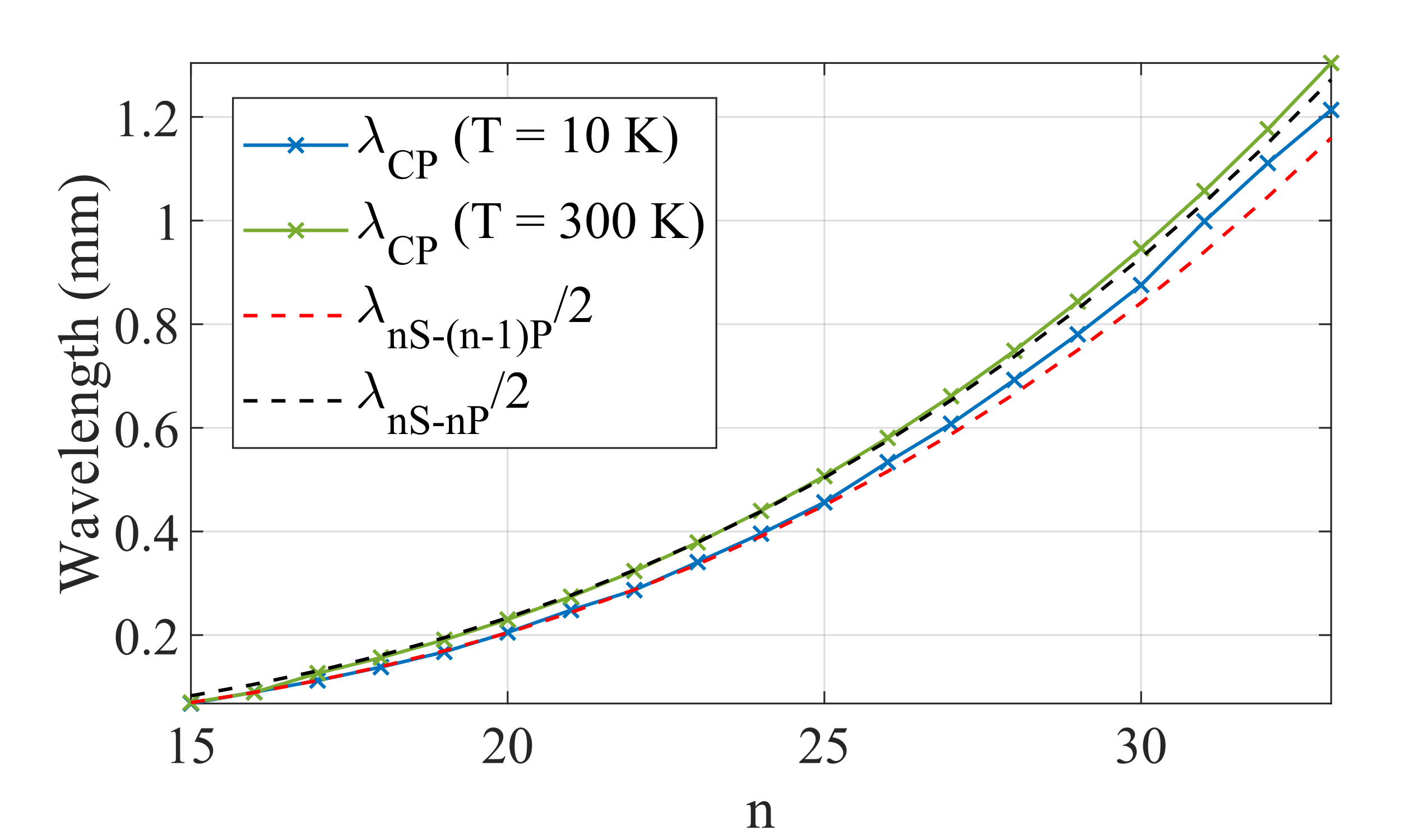
In the retarded regime, the CP potential exhibits oscillatory behavior determined by the dominant atomic transition frequencies: the wavelength of the spatial oscillation of the CP potential, , is roughly half the wavelength of the dominant transition frequencies, and (see Fig. 5). The oscillation starts when the atom-surface distance is approximately half the corresponding atomic transition wavelength, which can be seen, for example, at the distance indicated by the purple vertical line in Fig. 4. For low- states, the dominant transition frequencies are high, the CP potential starts to oscillate at short atom-surface distances around m; for high- states, the dominant transition frequencies are low with corresponding wavelengths of a few mm.
In order to quantify how each intermediate state in Eq. (6) contributes to the total resonant CP potential, we consider a relative contribution, , which is defined as the absolute value of each term (specified by ) divided by the summation of the absolute value of all terms in Eq. (6). The relative contributions of the four adjacent energy-states for 87Rb atom in the 15S state (m) at m, and m together with for the 13P and 14P states are shown versus atom-surface distances in Fig. 6. Since we know that the non-resonant potential is monotonic, the underlying mechanics of the oscillations of the CP potential must originate from the resonant term. The signs of the individual contributions alter with distances and at some points the positive and negative contributions cancel out each other, resulting in a negligible potential. We can also see that , indicating that this is the spectroscopic low-temperature regime. As a result, the contributions from all upward atomic transitions are negligible due to the lack of thermal photons.

IV.4 Temperature and Rydberg state dependence
Thermal effects on the CP potential of ground-state atoms and molecules depend on the dominant atomic transition frequencies, which determine the non-retarded and retarded types: the near-surface (order of m) CP potentials of molecules are likely to be non-retarded and hence insensitive to temperature as the dominant transition frequencies are low (), while the CP potentials for ground-state atoms are strongly retarded and thus greatly affected by temperature since the dominant transition frequencies are high () Ellingsen et al. 2009; Ellingsen et al. 2010; Klimchitskaya and Mostepanenko 2018.
First, we consider how the conductivity of graphene depends on temperature. There is an explicit linear temperature dependence in the non-resonant potential–see Eq. (5). The temperature dependence for the resonant term, Eq. (6), is embedded in the thermal photon distribution function, where as long as , i.e. the spectroscopic high-temperature limit. On the other hand, there are five quantities that depend on the principal quantum number as mentioned in Section IV.2.

Fig. 7 shows the variations of the CP potential with (a) principal quantum number, calculated at m and (b) temperature, calculated for the 40S state at m ( and ).
Even though, the non-resonant and resonant potential, each scales with , the total CP potential obeys an power law. The CP potential changes linearly with temperature. The reason is that the dominant transition energies of Rydberg atoms between two nearest energy-states, P and P, are small compared to thermal energy, , which makes the condition so the average photon number is reduced to , confirming a linear relation with as shown in panel (b).

We now consider how the resonant contributions change with the principal quantum number. In Fig. 8, we plot the contributions of the intermediate states to the resonant parts of the CP potential in the 25S, 30S, 35S, 40S and 45S states for the environment temperature . Note that the systems are in the non-retarded limit, and the spectroscopic temperature for the 25S state is approximately , slightly higher than the environment temperature, whereas for the 45S state, indicating the spectroscopic high-temperature limit. We can see that the contributions from the intermediate states to the resonant parts also change when the principal quantum number of the target state changes.
As shown in Fig. 8, the (downward-transition) contributions from the intermediate states with energy levels below the target states (below and including P state) get smaller as increases and vice versa for the intermediate states with higher energies (i.e. upward-transition contributions), which is captured in panel (f). In other words, the system approaches the spectroscopic high-temperature limit as increases, resulting in an increase in the repulsive resonant potential. This behaviour of the resonant parts will affect the scaling of the CP potential with and also enhances the temperature dependence of the upward-transition contributions as we shall see in more detail in Sec. V.
We now proceed to look into detail at how the resonant contributions from the two nearest energy states change with temperature. For the 20S state, there is a slight increase in the positive contribution from the 20P state as increases, while the opposite happens to the 19P state, as shown in Fig. 9(a), resulting in the evanescent-wave potential being more positive as increases. Fig. 9(b) shows the non-resonant and resonant contributions due to evanescent and propagating waves. The attractive contribution from the non-resonant part is stronger than the repulsive resonant potential.

IV.5 Effects of changing Fermi energy
In this section, we will investigate how the CP potential of single-layer graphene depends on its Fermi energy, which influences the conductivity of the graphene sheet and, hence, its reflection coefficients and underlying Green’s tensor. We expect stronger non-resonant contributions to the CP potential as we increase the Fermi energy since we are adding more conduction electrons. Regarding the resonant part, the dominant atomic transition frequencies of the atomic states usually considered are in the microwave-terahertz spectral regions, which are small compared to the typical Fermi energy. Consequently, as discussed in Appendix B, we expect that graphene’s optical conductivity will be dominated by the intraband-process term, which is almost linear in and is a few orders of magnitude higher than the universal AC conductivity of graphene , as shown in Fig. 10. However, the CP potential does not vary linearly with the Fermi energy as we can see in Fig. 11, where we show the CP potential calculated at (a) m and (b) m in the 30S state. In (a), at , the potential peaks at then decreases and rises again as the Fermi energy deviates from eV. This is not the case for and : the potential then gets more attractive as the doping level increases. In (b), all three curves exhibit similar behaviors: the potential is the most attractive at .


V Fitted empirical functions
In this section, we will try to find fitted empirical functions that follow the power laws discussed in the preceding sections. Let us begin by writing the CP potential in the form:
| (9) |
where is a positive dispersion coefficient and is a scaling power to be evaluated.
V.1 Low-temperature limit
We first consider the non-retarded, spectroscopic low-temperature limit in order to determine the scaling relation of the CP potential that largely depends on the atom-surface separation and on the principal quantum number. Figure 12 shows the CP potential at for (a) a m-thick gold sheet, (b) graphene modeled by the Kubo conductivity and (c) graphene modeled by the full non-local conductivity. Panel (d) shows the dispersion coefficients, , versus the principal quantum numbers. From the slopes of the CP potential in panels (a)-(c), is determined to be and it follows from the slopes of in panel (d) that approximately. To be more precise, assuming ( and are coefficients), we find, for the gold sheet,
| (10) |
for graphene modeled by the Kubo conductivity,
| (11) |
and for graphene modeled by the full non-local model,
| (12) |
Alternatively, if we assume that is proportional to a single power of , we find, for the gold sheet,
| (13) |
for graphene modeled by the Kubo conductivity,
| (14) |
and for graphene modeled by the full non-local model,
| (15) |
We can see from the above equations that both the Kubo and full non-local models give quantitatively similar results.

V.2 Including temperature-dependent effects

In this subsection, we try to include the scaling law of the CP potential with temperature in an attempt to find a more complete fitted empirical formula which can describe the CP potential of a 87Rb atom near a single graphene sheet in the non-retarded regime and for various . This is done by calculating the CP potential versus temperature to obtain the dispersion coefficient, , as a function of temperature, , and principal quantum number, , in the form of a linear equation . Figs. 13(a) and (b) show the CP potential near graphene vs for the 20S, 25S, 30S, 35S and 40S states and its associated dispersion coefficient, . The curves show a linear relationship between the potential and temperature. However, the slopes of the and curves become steeper as increases since the positive resonant contributions increase as increases, as shown in Fig. 8. The non-linear relations between the coefficients, and , and are shown in Figs. 13(c) and (d). We can fit them with polynomial equations of degree and as follows (see Sec. IV.2):
| (16) |
| (17) |
We may write the fitted empirical function for the CP potential for graphene-monolayer in the spectroscopic high-temperature and non-retarded regime as
| (18) |
V.3 Accuracy of the fitted empirical functions
We now check the accuracy of our fitted empirical formula, Eq.(18), compared with the general formula, Eq. (4), by plotting the CP potential for atom-surface distances in the range m to m and calculating the absolute values of the energy differences.
Fig. 14 shows the CP potential calculated by the general formula (blue solid curves) and the empirical formula (orange dashed curves), together with their corresponding energy differences, , at (a, c) and (b, d) . We can see that the empirical formula gives results that are off by at m. Beyond this point, the differences are of order smaller than Megahertz. The empirical formula provides the least accurate results for the 20S state with a relative error as high as . As for the other two states, the relative error is far below .

VI Heterostructures containing two graphene layers
In this section, we study the CP potential of heterostructures containing two separated layers of graphene, which provide a wider range of tuneable optical properties than single-layer graphene (SLG) Rodrigo et al. 2017; Woessner et al. 2014; Brar et al. 2014.
Hexagonal boron nitride (hBN) is commonly used to integrate with graphene to form complex structures; we can use it, for example, as a substrate, a tunnel barrier Geim and Grigorieva 2013, or an encapsulating layer Thomsen et al. 2017; Han et al. 2019. We can grow hBN on graphene vertically Yankowitz et al. 2014 or laterally Wrigley et al. 2021.
Let us consider a simple van der Waals (vdW) heterostructure comprising an hBN layer with permittivity Laturia et al. 2018 sandwiched between two graphene monolayers with spacing between them. Bare graphene layers (i.e. without an hBN spacer) in vacuum will also be considered as a comparison. Figure 15 shows the CP potential of the said structures at and m for a 87Rb atom in the 30S state. In (a), the spacing is varied between nm and m; the potential becomes more negative when we increase the spacing between two graphene layers until for the graphene-vacuum-graphene structure and for the graphene-hBN-graphene structure, when the potential gets less negative again. In (b), we show that the potential of the structure containing two layers of graphene approaches that of the single-layered one as is increased to m.

In order to show the relationship between and , in Fig. 16 we plot the color map of the differences (in kHz) between the CP potential of SLG and that of graphene-vacuum-graphene structure on a linear-log scale. We can see once again that the behavior of the two-graphene-layered structure approaches that of SLG as the spacing increases and that the atom effectively experiences the two-graphene-layered structure as SLG when the atom-surface distance is large enough.

Now let us consider how the CP potential changes when we simultaneously vary the Fermi levels of the top and bottom graphene layers. As a background, for a ground-state atom near two layers of graphene, the CP potential generally becomes more attractive as graphene sheets are electrically doped Ribeiro and Scheel 2013. Figure 17 shows the CP potential (in MHz) versus the Fermi energies of the top and bottom layer of the graphene-hBN-graphene structure for a 87Rb atom in the 30S state at T = , taking m and . We can see that in the middle of the colour map where the Fermi energies of both layers are zero, the potential is still stronger than in most regions of the parameter plane. Moreover, it is very surprising that the potential is the most attractive when of the top layer is zero. This cannot simply be explained by considering the conductivity alone; in addition the non-resonant and resonant terms are enhanced differently when the Fermi energies are varied.
Lastly, let us investigate how the CP potential depends on the spacing and on the Fermi energy of the top layer when the Fermi energy of the bottom layer is fixed. Figure 18 shows the CP potential (in MHz) of the graphene-vacuum-graphene structure calculated versus the spacing between the graphene layers (in a logarithmic scale) and the Fermi energy of the top layer when the Fermi energy of the bottom layer is set to at = and m. We may divide the behavior of the CP potential landscape into three regimes: the first is the SLG-like regime, in which the separation between the two graphene layers is large. In this regime, the potential becomes more negative when the Fermi energy is increased. The second regime is when -; the potential then barely changes with Fermi energy. The third regime is when . In this regime, the potential is the most attractive when .


VII Conclusions
In summary, we have calculated and analyzed the CP potential of a rubidium Rydberg atom positioned near single-layer and double-layer graphene. These calculations used a Green’s-function method in the framework of macroscopic quantum electrodynamics. The optical conductivity of the layer(s) was modeled by the local Kubo equation, including non-local effects. Together, the atomic electric polarizability, the dipole matrix elements of the atom, and the electromagnetic reflection coefficients of the surface layer(s), determine the CP potential. Since Rydberg atoms have higher electric polarizabilities than, and their dipole matrix elements between adjacent atomic states exceed, those of ground-state atoms, their CP potential interaction with graphene-based multilayers is complex.
We have shown that, at in the non-retarded regime, the CP potential of monolayer graphene is weaker than that for a -m-thick gold sheet for low- states, but the CP potential of graphene becomes increasingly attractive when . Regarding the different models of graphene’s conductivity, the near-surface potential calculated using the local conductivity is slightly more attractive than that calculated from the full non-local conductivity models for typical doping levels () and . In general, in the non-retarded limit, the CP potential is determined by both the monotonic attractive non-resonant potential and the evanescent-wave resonant potential. In the retarded limit, the CP potential is dominated by the resonant potential alone and spatially oscillates with a periodicity that approximately equals the half wavelength of the nearest downward transition at low temperature and the nearest upward transition at high temperature. The spatial oscillations in the CP potential start to occur when the atom-surface separation begins to exceed these wavelengths. Thermal effects come into play when the thermal energy is resonant with the atomic transition energies. In the non-retarded, spectroscopic low-temperature limit, the atomic transitions are dominated by downward transitions, which give rise to an attractive resonant potential. In contrast, in the spectroscopic high-temperature limit, there are enough thermal photons to stimulate upward transitions, resulting in a repulsive potential. The spectroscopic high-temperature limit can be easily realized by increasing the principal quantum number even below room temperature. Doping graphene generally results in a more attractive CP potential at high temperatures.
Finally, we have investigated heterostructures containing two graphene sheets with varying inter-layer separation and Fermi energies. We found that the effects of changing the spacing and Fermi energies are inter-related. When the spacing is small (m), doping the top layer either positively or negatively weakens the CP potential. By contrast, when the spacing is large the behavior approaches that of single-layer graphene.
Possible future work could be done on multiple-layer structures comprising graphene and other 2D materials. The complex interference of electromagnetic waves within and near such structures could greatly affect the resonant CP potential. Studying the many-body effects of Rydberg atoms near graphene-based heterostructures might also be interesting since parameters such as the layer chemical potentials, inter-layer spacing, and/or the number and type of 2D layers can be altered to manipulate the interaction with, and behavior of, nearby trapped atoms.
Acknowledgements: This work is supported by the EPSRC through Grant No. EP/R04340X/1 via the QuantERA project “ERyQSenS”.
Appendix A Green’s tensor
An electric field created by a radiating electric dipole can be described by a classical Green’s tensor whose form for planar multilayered systems is well-known. When analysing the resonant part of the CP potential, it is useful to split the equal-position scattering Green’s tensor into evanescent-wave and propagating-wave components as follows Buhmann 2012; Amorim et al. 2017:
| (19) |
The evanescent-wave component takes the form
| (20) |
and the propagating-wave component takes the form
| (21) |
where is the shortest distance between the surface and the center of the atom, and are the Fresnel reflection coefficients for the - and -polarized waves, respectively, and
| (22) |
| (23) | ||||
| (24) |
Appendix B Graphene’s Optical Properties
B.1 Conductivity models
In this section, we present two models for the optical conductivity of monolayer graphene: (i) based on local Kubo conductivity, , which depends only on the angular frequencies, , of the incident electromagnetic radiations and ignores spatial dispersion in the graphene surface Gonçalves and Peres 2016; Stauber et al. 2008; Hanson 2013 and (ii) using the full non-local conductivity, , which is derived from the Lindhard polarisation function in random-phase (RPA) and relaxation-time (RT) approximations Lindhard 1954; Wunsch et al. 2006; Hwang and Das Sarma 2007; Gonçalves and Peres 2016. The latter takes into account spatial dispersion by non-local causes when considering the interactions of incident photons, surface plasmons with wavenumbers, , and graphene’s electrons.
The Kubo conductivity can be expressed as the sum of two contributions: , which arises from intraband transition processes of the electrons and , which describes transitions between the conduction and valence bands; both terms may be written as follows:
| (25) |
| (26) |
in which
| (27) |
where is the universal alternating-current conductivity of graphene, is the electron relaxation rate in graphene, is the Fermi energy and is the temperature of the graphene layer.
As for the other model–the full non-local conductivity, we start by providing the 2D polarizability in the RPA, , in the limit, where and are the real and imaginary parts, respectively, in six regions of the -space as depicted in Fig. 19 as follows:

region 1A
| (28) | ||||
| (29) |
region 2A
| (30) | ||||
| (31) |
region 3A
| (32) | ||||
| (33) |
region 1B
| (34) | ||||
| (35) |
region 2B
| (36) | ||||
| (37) |
region 3B
| (38) | ||||
| (39) |
where , , , , , , , . Here and are Fermi velocity and wavenumbers, respectively. The auxiliary functions are defined as follows
| (40) | ||||
| (41) |
The 2D polarizability described above only takes into account intrinsic mechanisms for the decay of GSP into electron-hole pairs. To include extrinsic processes such as collisions with lattice defects or impurity scattering, we extend the previous model by also including scattering events within the relaxation-time approximation, which allows us to express the 2D polarizability in the RPA-RT approximation as follows:
| (42) |
The RPA-RT dielectric function can be written in terms of the 2D polarisation function as
| (43) |
where is the relative permittivity of the medium in which the graphene layer is embedded and is the Fourier transform of the Coulomb interaction. Additionally, the longitudinal conductivity can also be written in terms of the Lindhard polarizability:
| (44) |
Note that it is this quantity–the conductivity–that will be inserted into our transfer-matrix calculations of the reflection coefficients of graphene, when we calculate the CP potential.

Appendix C Permittivity of metals
The permittivity of gold at radiation frequency is described by the Drude model Ashcroft and Mermin 1976
| (45) |
where, for gold, is the plasma frequency and is the electron scattering rate Zeman and Schatz 1987.
References
- Chen and Fan [2020] X. Chen and B. Fan, Reports on Progress in Physics 83, 076401 (2020).
- Liu et al. [2018] L. Liu, D.-S. Lü, W.-B. Chen, T. Li, Q.-Z. Qu, B. Wang, L. Li, W. Ren, Z.-R. Dong, and J.-B. e. a. Zhao, Nature Communications 9, 2760 (2018).
- Ren et al. [2020] W. Ren, T. Li, Q. Qu, B. Wang, L. Li, D. Lü, W. Chen, and L. Liu, National Science Review 7, 1828 (2020).
- Knight and Walmsley [2019] P. Knight and I. Walmsley, Quantum Sci. Technol. 4, 040502 (2019).
- Acín et al. [2018] A. Acín, I. Bloch, H. Buhrman, T. Calarco, C. Eichler, J. Eisert, D. Esteve, N. Gisin, S. Glaser, F. Jelezko, S. Kuhr, M. Lewenstein, M. Riedel, P. Schmidt, R. Thew, A. Wallraff, I. Walmsley, and F. Wilhelm, New J. Phys. 20, 080201 (2018).
- Meinert et al. [2020] F. Meinert, C. Hölzl, M. A. Nebioglu, A. D’Arnese, P. Karl, M. Dressel, and M. Scheffler, Phys. Rev. Research 2, 023192 (2020).
- Geier et al. [2021] S. Geier, N. Thaicharoen, C. Hainaut, T. Franz, A. Salzinger, A. Tebben, D. Grimshandl, G. Zürn, and M. Weidemüller, Science 374, 1149 (2021).
- Haug et al. [2019] T. Haug, S. Y. Buhmann, and R. Bennett, Phys. Rev. A 99, 012508 (2019).
- Scheel et al. [2005] S. Scheel, P. K. Rekdal, P. L. Knight, and E. A. Hinds, Phys. Rev. A 72, 042901 (2005).
- Rekdal et al. [2004] P. K. Rekdal, S. Scheel, P. L. Knight, and E. A. Hinds, Phys. Rev. A 70, 013811 (2004).
- Folman et al. [2002] R. Folman, P. Krüger, J. Schmiedmayer, J. Denschlag, and C. Henkel, Advances In Atomic, Molecular, and Optical Physics , 263 (2002).
- Henkel et al. [1999] C. Henkel, S. Pötting, and M. Wilkens, Applied Physics B 69, 379 (1999).
- Hinds and Hughes [1999] E. A. Hinds and I. G. Hughes, Journal of Physics D: Applied Physics 32, R119 (1999).
- Jones et al. [2003] M. P. A. Jones, C. J. Vale, D. Sahagun, B. V. Hall, and E. A. Hinds, Phys. Rev. Lett. 91, 080401 (2003).
- Messina and Passante [2007] R. Messina and R. Passante, Phys. Rev. A 76, 032107 (2007).
- Vasile and Passante [2008] R. Vasile and R. Passante, Phys. Rev. A 78, 032108 (2008).
- Ferreri et al. [2019] A. Ferreri, M. Domina, L. Rizzuto, and R. Passante, Symmetry 11 (2019).
- Laliotis et al. [2021a] A. Laliotis, B.-S. Lu, M. Ducloy, and D. Wilkowski, AVS Quantum Science 3, 043501 (2021a).
- Sinuco-León et al. [2011] G. Sinuco-León, B. Kaczmarek, P. Krüger, and T. M. Fromhold, Phys. Rev. A 83, 021401 (2011).
- Sinuco-León et al. [2018] G. Sinuco-León, P. Krüger, and T. Fromhold, Journal of Modern Optics 65, 677 (2018).
- Aigner et al. [2008] S. Aigner, L. D. Pietra, Y. Japha, O. Entin-Wohlman, T. David, R. Salem, R. Folman, and J. Schmiedmayer, Science 319, 1226 (2008).
- Japha et al. [2008] Y. Japha, O. Entin-Wohlman, T. David, R. Salem, S. Aigner, J. Schmiedmayer, and R. Folman, Phys. Rev. B 77, 201407 (2008).
- Schumm et al. [2005] T. Schumm, J. Estève, C. Figl, J.-B. Trebbia, C. Aussibal, H. Nguyen, D. Mailly, I. Bouchoule, C. I. Westbrook, and A. Aspect, The European Physical Journal D 32, 171 (2005).
- Henkel et al. [2003] C. Henkel, P. Krüger, R. Folman, and J. Schmiedmayer, Applied Physics B: Lasers and Optics 76, 173 (2003).
- Lin et al. [2004] Y.-j. Lin, I. Teper, C. Chin, and V. Vuletić, Phys. Rev. Lett. 92, 050404 (2004).
- Laliotis et al. [2021b] A. Laliotis, B.-S. Lu, M. Ducloy, and D. Wilkowski, AVS Quantum Science 3, 043501 (2021b).
- Wongcharoenbhorn et al. [2021] K. Wongcharoenbhorn, R. Crawford, N. Welch, F. Wang, G. Sinuco-León, P. Krüger, F. Intravaia, C. Koller, and T. M. Fromhold, Phys. Rev. A 104, 053108 (2021).
- Ergoktas et al. [2021] M. Ergoktas, G. Bakan, E. Kovalska, L. Le Fevre, R. Fields, P. Steiner, X. Yu, O. Salihoglu, S. Balci, V. Fal’ko, K. Novoselov, R. Dryfe, and C. Kocabas, Nature Photonics 15, 493 (2021).
- Liu et al. [2020a] M. Liu, Z. Li, X. Zhao, R. Young, and I. Kinloch, Nano Letters 21, 833 (2020a).
- Kim et al. [2020] Y. Kim, T. Kim, J. Lee, Y. S. Choi, J. Moon, S. Y. Park, T. H. Lee, H. K. Park, S. A. Lee, and M. S. e. a. Kwon, Advanced Materials 33, 2004827 (2020).
- Carvalho et al. [2021] A. F. Carvalho, B. Kulyk, A. J. S. Fernandes, E. Fortunato, and F. M. Costa, Advanced Materials , 2101326 (2021).
- Mišeikis et al. [2020] V. Mišeikis, S. Marconi, M. A. Giambra, A. Montanaro, L. Martini, F. Fabbri, S. Pezzini, G. Piccinini, S. Forti, B. Terrés, I. Goykhman, L. Hamidouche, P. Legagneux, V. Sorianello, A. C. Ferrari, F. H. L. Koppens, M. Romagnoli, and C. Coletti, ACS Nano 14, 11190 (2020).
- Gosciniak et al. [2020] J. Gosciniak, M. Rasras, and J. B. Khurgin, ACS Photonics 7, 488 (2020).
- Gosciniak and Khurgin [2020] J. Gosciniak and J. B. Khurgin, ACS Omega 5, 14711 (2020).
- Zhu et al. [2021] Y. Zhu, H. Xu, P. Yu, and Z. Wang, Applied Physics Reviews 8, 021305 (2021).
- AlAloul and Rasras [2021] M. AlAloul and M. Rasras, J. Opt. Soc. Am. B 38, 602 (2021).
- Britnell et al. [2013] L. Britnell, R. V. Gorbachev, A. K. Geim, L. A. Ponomarenko, A. Mishchenko, M. T. Greenaway, T. M. Fromhold, K. S. Novoselov, and L. Eaves, Nature Communications 4, 1794 (2013).
- Liu et al. [2020b] L. Liu, Y. Liu, and X. Duan, Science China Information Sciences 63, 201401 (2020b).
- Ribeiro and Terças [2016] S. Ribeiro and H. Terças, Phys. Rev. A 94, 043420 (2016).
- Candussio et al. [2021] S. Candussio, M. V. Durnev, S. Slizovskiy, T. Jötten, J. Keil, V. V. Bel’kov, J. Yin, Y. Yang, S.-K. Son, A. Mishchenko, V. Fal’ko, and S. D. Ganichev, Phys. Rev. B 103, 125408 (2021).
- Tripathi et al. [2021] M. Tripathi, F. Lee, A. Michail, D. Anestopoulos, J. G. McHugh, S. P. Ogilvie, M. J. Large, A. A. Graf, P. J. Lynch, J. Parthenios, K. Papagelis, S. Roy, M. A. S. R. Saadi, M. M. Rahman, N. M. Pugno, A. A. K. King, P. M. Ajayan, and A. B. Dalton, ACS Nano 15, 2520 (2021).
- Ta et al. [2020] H. Q. Ta, A. Bachmatiuk, R. G. Mendes, D. J. Perello, L. Zhao, B. Trzebicka, T. Gemming, S. V. Rotkin, and M. H. Rümmeli, Advanced Materials 32, 2002755 (2020).
- Wei et al. [2021] T. Wei, F. Hauke, and A. Hirsch, Advanced Materials 33, 2104060 (2021).
- Cui et al. [2021a] L. Cui, J. Wang, and M. Sun, Reviews in Physics 6, 100054 (2021a).
- Liu et al. [2021a] M. Liu, Y. Zhang, G. L. Klimchitskaya, V. M. Mostepanenko, and U. Mohideen, Phys. Rev. B 104, 085436 (2021a).
- Slizovskiy et al. [2021] S. Slizovskiy, A. Garcia-Ruiz, A. I. Berdyugin, N. Xin, T. Taniguchi, K. Watanabe, A. K. Geim, N. D. Drummond, and V. I. Fal’ko, Nano Letters 21, 6678 (2021).
- Greenaway et al. [2021] M. T. Greenaway, P. Kumaravadivel, J. Wengraf, L. A. Ponomarenko, A. I. Berdyugin, J. Li, J. H. Edgar, R. K. Kumar, A. K. Geim, and L. Eaves, Nature Communications 12, 6392 (2021).
- McCann [2012] E. McCann, Electronic Properties of Monolayer and Bilayer Graphene (Springer Berlin Heidelberg, 2012) pp. 237–275.
- Fermani et al. [2007] R. Fermani, S. Scheel, and P. L. Knight, Phys. Rev. A 75, 062905 (2007).
- Thomsen et al. [2017] J. D. Thomsen, T. Gunst, S. S. Gregersen, L. Gammelgaard, B. S. Jessen, D. M. A. Mackenzie, K. Watanabe, T. Taniguchi, P. Bøggild, and T. J. Booth, Phys. Rev. B 96, 014101 (2017).
- Ju et al. [2011] L. Ju, B. Geng, J. Horng, C. Girit, M. Martin, Z. Hao, H. A. Bechtel, X. Liang, A. Zettl, Y. R. Shen, and F. Wang, Nature Nanotechnology 6, 630 (2011).
- Yan et al. [2013] H. Yan, T. Low, W. Zhu, Y. Wu, M. Freitag, X. Li, F. Guinea, P. Avouris, and F. Xia, Nature Photonics 7, 394 (2013).
- Cui et al. [2021b] L. Cui, J. Wang, and M. Sun, Reviews in Physics 6, 100054 (2021b).
- Haakh et al. [2014] H. R. Haakh, C. Henkel, S. Spagnolo, L. Rizzuto, and R. Passante, Phys. Rev. A 89, 022509 (2014).
- Zeng and Zubairy [2021] X. Zeng and M. S. Zubairy, Phys. Rev. Lett. 126, 117401 (2021).
- Cysne et al. [2014] T. Cysne, W. J. M. Kort-Kamp, D. Oliver, F. A. Pinheiro, F. S. S. Rosa, and C. Farina, Phys. Rev. A 90, 052511 (2014).
- Liu et al. [2021b] M. Liu, Y. Zhang, G. L. Klimchitskaya, V. M. Mostepanenko, and U. Mohideen, Phys. Rev. B 104, 085436 (2021b).
- Henkel et al. [2018] C. Henkel, G. L. Klimchitskaya, and V. M. Mostepanenko, Phys. Rev. A 97, 032504 (2018).
- Chaichian et al. [2012] M. Chaichian, G. L. Klimchitskaya, V. M. Mostepanenko, and A. Tureanu, Phys. Rev. A 86, 012515 (2012).
- Churkin et al. [2010] Y. V. Churkin, A. B. Fedortsov, G. L. Klimchitskaya, and V. A. Yurova, Phys. Rev. B 82, 165433 (2010).
- Bordag et al. [2006] M. Bordag, B. Geyer, G. L. Klimchitskaya, and V. M. Mostepanenko, Phys. Rev. B 74, 205431 (2006).
- Cysne et al. [2016] T. P. Cysne, T. G. Rappoport, A. Ferreira, J. M. V. P. Lopes, and N. M. R. Peres, Phys. Rev. B 94, 235405 (2016).
- Nichols et al. [2016] N. S. Nichols, A. Del Maestro, C. Wexler, and V. N. Kotov, Phys. Rev. B 93, 205412 (2016).
- Klimchitskaya and Mostepanenko [2020] G. L. Klimchitskaya and V. M. Mostepanenko, Universe 6, 150 (2020).
- Kaur et al. [2014] K. Kaur, J. Kaur, B. Arora, and B. K. Sahoo, Phys. Rev. B 90, 245405 (2014).
- Khusnutdinov et al. [2018] N. Khusnutdinov, R. Kashapov, and L. M. Woods, 2D Materials 5, 035032 (2018).
- Šibalić and Adams [2018] N. Šibalić and C. S. Adams, Rydberg Physics, 2399-2891 (IOP Publishing, 2018).
- Kohlhoff [2016] M. W. Kohlhoff, The European Physical Journal Special Topics 225, 3061 (2016).
- Hermann-Avigliano et al. [2014] C. Hermann-Avigliano, R. C. Teixeira, T. L. Nguyen, T. Cantat-Moltrecht, G. Nogues, I. Dotsenko, S. Gleyzes, J. M. Raimond, S. Haroche, and M. Brune, Phys. Rev. A 90, 040502 (2014).
- Wu et al. [2021] X. Wu, X. Liang, Y. Tian, F. Yang, C. Chen, Y.-C. Liu, M. K. Tey, and L. You, Chinese Physics B 30, 020305 (2021).
- Ellingsen et al. [2010] S. A. Ellingsen, S. Y. Buhmann, and S. Scheel, Phys. Rev. Lett. 104, 223003 (2010).
- Törmä and Barnes [2014] P. Törmä and W. L. Barnes, Reports on Progress in Physics 78, 013901 (2014).
- Kübler et al. [2013] H. Kübler, D. Booth, J. Sedlacek, P. Zabawa, and J. P. Shaffer, Phys. Rev. A 88, 043810 (2013).
- Ribeiro et al. [2013] S. Ribeiro, S. Y. Buhmann, and S. Scheel, Phys. Rev. A 87, 042508 (2013).
- Sheng et al. [2016] J. Sheng, Y. Chao, and J. P. Shaffer, Phys. Rev. Lett. 117, 103201 (2016).
- Barton [1974] G. Barton, Journal of Physics B: Atomic and Molecular Physics 7, 2134 (1974).
- Power and Thirunamachandran [1982] E. A. Power and T. Thirunamachandran, Phys. Rev. A 25, 2473 (1982).
- Barton [1988] G. Barton, Physica Scripta T21, 11 (1988).
- Meschede et al. [1990] D. Meschede, W. Jhe, and E. A. Hinds, Phys. Rev. A 41, 1587 (1990).
- Hinds and Sandoghdar [1991] E. A. Hinds and V. Sandoghdar, Phys. Rev. A 43, 398 (1991).
- Bambini and Robinson [1992] A. Bambini and E. J. Robinson, Phys. Rev. A 45, 4661 (1992).
- Fichet et al. [1995] M. Fichet, F. Schuller, D. Bloch, and M. Ducloy, Phys. Rev. A 51, 1553 (1995).
- Gorza et al. [2001] M.-P. Gorza, S. Saltiel, H. Failache, and M. Ducloy, The European Physical Journal D 15, 113 (2001).
- Bushev et al. [2004] P. Bushev, A. Wilson, J. Eschner, C. Raab, F. Schmidt-Kaler, C. Becher, and R. Blatt, Phys. Rev. Lett. 92, 223602 (2004).
- Buhmann et al. [2004] S. Y. Buhmann, L. Knöll, D.-G. Welsch, and H. T. Dung, Phys. Rev. A 70, 052117 (2004).
- Gorza and Ducloy [2006] M.-P. Gorza and M. Ducloy, The European Physical Journal D 40, 343 (2006).
- Buhmann and Welsch [2008] S. Y. Buhmann and D.-G. Welsch, Phys. Rev. A 77, 012110 (2008).
- Schiefele and Henkel [2010] J. Schiefele and C. Henkel, Phys. Rev. A 82, 023605 (2010).
- Crosse et al. [2010] J. A. Crosse, S. Å. Ellingsen, K. Clements, S. Y. Buhmann, and S. Scheel, Phys. Rev. A 82, 010901 (2010).
- Antezza et al. [2014] M. Antezza, C. Braggio, G. Carugno, A. Noto, R. Passante, L. Rizzuto, G. Ruoso, and S. Spagnolo, Phys. Rev. Lett. 113, 023601 (2014).
- Ribeiro et al. [2015] S. Ribeiro, S. Y. Buhmann, T. Stielow, and S. Scheel, EPL (Europhysics Letters) 110, 51003 (2015).
- Armata et al. [2016] F. Armata, R. Vasile, P. Barcellona, S. Y. Buhmann, L. Rizzuto, and R. Passante, Phys. Rev. A 94, 042511 (2016).
- Carvalho et al. [2018] J. C. d. A. Carvalho, P. Pedri, M. Ducloy, and A. Laliotis, Phys. Rev. A 97, 023806 (2018).
- Yang et al. [2019] B. Yang, B. Zhang, Z. Liu, and H. Yao, Journal of Physics B: Atomic, Molecular and Optical Physics 52, 095501 (2019).
- Fang et al. [2019] W. Fang, G.-X. Li, J. Xu, and Y. Yang, Opt. Express 27, 37753 (2019).
- Buhmann et al. [2021] S. Y. Buhmann, S. M. Giesen, M. Diekmann, R. Berger, S. Aull, P. Zahariev, M. Debatin, and K. Singer, New Journal of Physics 23, 083040 (2021).
- Fuchs et al. [2018] S. Fuchs, R. Bennett, and S. Y. Buhmann, Phys. Rev. A 98, 022514 (2018).
- Wilson et al. [2003] M. A. Wilson, P. Bushev, J. Eschner, F. Schmidt-Kaler, C. Becher, R. Blatt, and U. Dorner, Phys. Rev. Lett. 91, 213602 (2003).
- Barcellona et al. [2016] P. Barcellona, R. Passante, L. Rizzuto, and S. Y. Buhmann, Phys. Rev. A 93, 032508 (2016).
- Ribeiro and Scheel [2013] S. Ribeiro and S. Scheel, Phys. Rev. A 88, 042519 (2013).
- M. et al. [2011] M. M. M., H. R. Haakh, T. Calarco, C. P. Koch, and C. Henkel, Quantum Information Processing 10, 771 (2011).
- Wade et al. [2016] C. G. Wade, Šibalić N., N. R. de Melo, J. M. Kondo, C. S. Adams, and K. J. Weatherill, Nature Photonics 11, 40 (2016).
- Saffman [2016] M. Saffman, Journal of Physics B: Atomic, Molecular and Optical Physics 49, 202001 (2016).
- Scheel and Buhmann [2009] S. Scheel and S. Y. Buhmann, Phys. Rev. A 80, 042902 (2009).
- Scheel and Buhmann [2008] S. Scheel and S. Buhmann, Acta Physica Slovaca. 58, 675 (2008).
- Buhmann [2012] S. Y. Buhmann, Dispersion Forces II: Many-Body Effects, Excited Atoms, Finite Temperature and Quantum Friction (Springer, Berlin, 2012).
- Buhmann and Scheel [2008] S. Y. Buhmann and S. Scheel, Phys. Rev. Lett. 100, 253201 (2008).
- Gallagher [1988] T. F. Gallagher, Reports on Progress in Physics 51, 143 (1988).
- Seaton [1983] M. J. Seaton, Reports on Progress in Physics 46, 167 (1983).
- Robertson et al. [2021] E. Robertson, N. Šibalić, R. Potvliege, and M. Jones, Computer Physics Communications 261, 107814 (2021).
- Numerov [1927] B. Numerov, Astronomische Nachrichten 230, 359 (1927).
- Li et al. [2003] W. Li, I. Mourachko, M. W. Noel, and T. F. Gallagher, Phys. Rev. A 67, 052502 (2003).
- Gric [2019] T. Gric, Opt Quant Electron 51, 202 (2019).
- Andryieuski and Lavrinenko [2013] A. Andryieuski and A. V. Lavrinenko, Optics Express 21, 9144 (2013).
- Gonçalves and Peres [2016] P. A. D. Gonçalves and N. M. R. Peres, An Introduction to Graphene Plasmonics (World Scientific, Singapore, 2016).
- Amorim et al. [2017] B. Amorim, P. A. D. Gonçalves, M. I. Vasilevskiy, and N. M. R. Peres, Applied Sciences 7, 1158 (2017).
- Ellingsen et al. [2009] S. A. Ellingsen, S. Y. Buhmann, and S. Scheel, Phys. Rev. A 79, 052903 (2009).
- Klimchitskaya and Mostepanenko [2018] G. L. Klimchitskaya and V. M. Mostepanenko, Phys. Rev. A 98, 032506 (2018).
- Rodrigo et al. [2017] D. Rodrigo, A. Tittl, O. Limaj, F. J. G. d. Abajo, V. Pruneri, and H. Altug, Light: Science & Applications 6, 10.1038/lsa.2016.277 (2017).
- Woessner et al. [2014] A. Woessner, M. B. Lundeberg, Y. Gao, A. Principi, P. Alonso-González, M. Carrega, K. Watanabe, T. Taniguchi, G. Vignale, M. Polini, and et al., Nature Materials 14, 421 (2014).
- Brar et al. [2014] V. W. Brar, M. S. Jang, M. Sherrott, S. Kim, J. J. Lopez, L. B. Kim, M. Choi, and H. Atwater, Nano Letters 14, 3876 (2014), publisher: American Chemical Society.
- Geim and Grigorieva [2013] A. K. Geim and I. V. Grigorieva, Nature 499, 419 (2013).
- Han et al. [2019] X. Han, J. Lin, J. Liu, N. Wang, and D. Pan, The Journal of Physical Chemistry C 123, 14797 (2019).
- Yankowitz et al. [2014] M. Yankowitz, J. Xue, and B. J. LeRoy, Journal of Physics: Condensed Matter 26, 303201 (2014).
- Wrigley et al. [2021] J. Wrigley, J. Bradford, T. James, T. S. Cheng, J. Thomas, C. J. Mellor, A. N. Khlobystov, L. Eaves, C. T. Foxon, S. V. Novikov, and P. H. Beton, 2D Materials 8, 034001 (2021).
- Laturia et al. [2018] A. Laturia, M. L. Van de Put, and W. G. Vandenberghe, npj 2D Materials and Applications 2, 10.1038/s41699-018-0050-x (2018).
- Stauber et al. [2008] T. Stauber, N. M. R. Peres, and A. K. Geim, Phys. Rev. B 78, 085432 (2008).
- Hanson [2013] G. W. Hanson, Journal of Applied Physics 113, 029902 (2013).
- Lindhard [1954] J. Lindhard, Dan. Mat. Fys. Medd. 28, 1 (1954).
- Wunsch et al. [2006] B. Wunsch, T. Stauber, F. Sols, and F. Guinea, New Journal of Physics 8, 318 (2006).
- Hwang and Das Sarma [2007] E. H. Hwang and S. Das Sarma, Phys. Rev. B 75, 205418 (2007).
- Ashcroft and Mermin [1976] N. W. Ashcroft and N. D. Mermin, Solid State Physics (Saunders College Publishing, 1976).
- Zeman and Schatz [1987] E. J. Zeman and G. C. Schatz, The Journal of Physical Chemistry 91, 634 (1987).