Topological semimetal phases in a family of monolayer X3YZ6 (X=Nb,Ta, Y=Si,Ge,Sn, Z=S,Se,Te) with abundant nodal lines and nodes
Abstract
The electronic and topological properties of single-layer X3YZ6 (X=Nb,Ta, Y=Si,Ge,Sn, Z=S,Se,Te) materials have been studied with the aid of first principles calculations. This kind of materials belong to topological semimetals (TMs) with abundant nodal lines and nodes. Considering their similar properties, we focus on the analysis of Ta3SnTe6 and Ta3SiSe6. The present of spin-orbit coupling (SOC) leads to the transition from type-I nodal lines to Dirac points as well as the disappear of type-II Dirac points. The three-dimensional (3D) band diagrams reproduce vividly the characteristics of nodes and nodal lines. The appearance of the flat bands in (110) edge states further confirm their nontrivial topological properties. We also explore the relationship among different nodal lines (nodes), crystal symmetry and SOC. The type-I nodal lines are protected by Mz and symmetry in the absent of SOC. Symmetry breaking leads to band splitting even in the presence of SOC. The single-layer X3YZ6 can be used as candidates for two-dimensional (2D) TMs and provide a platform for further study of interesting physical phenomena.
pacs
61.46.-w,61.50.Ah,73.20.AtI. Introduction
With the development of topological materials, topological semimetals (TSMs) have become one of the hottest topics in condensed matter physicsgra1; gra2; d1; d2; d3; wl1; wl2; nl1; nl2; nl3; nl4; sm1; sm2; sm3; mp1; mp2, originating from the character of symmetrically or topologically protected band degeneracy near Fermi energy and potential applications. Based on the band crossing points near the Fermi energy, TSMs can be divided into Dirac semimetals (DSMs)d1; d2; d3, Weyl semimetals (WSMs)wl1; wl2, nodal line semimetals (NLSMs)nl1; nl2; nl3 and multiple degenerate points semimetalssm1; sm2; mp1; mp2. DSMs have fourfold degenerate band touching points with Dirac cones surface states. WSMs possess twofold degenerate band crosspoint with Fermi-arc surface states. NLSMs are the special cases of DSMs and WSMs with continuously distributed band intersections and drumhead surface states, forming closed ring, nodal links, nodal knots or nodal chainsnl4. Na3Bi, Cd3As2ex1; ex2 and TaAs familywl2; taas1; taas2; taas3 are the earlier experimentally discovered DSMs or WSMs materials. In addition, NLSMs have also been verified by experimentpbtase; comngaand host many unusual behavior, such as ultrahigh mobility1, possible high temperature superconductivity2 and the abnormal optical response3. Although more and more TSMs are theoretically predicted, most of them lack experimental validation, especially the two-dimensional (2D) NLSMs, whose experimental observation conditions are more demanding. Therefore, it is urgent to propose the TSMs candidate materials for experimental implementation.
Recently, Nb3GeTe6 and Nb3SiTe6 have attracted a great deal of attention because of their nontrivial topological propertiesta1; ta2; ta3; ta4; ta5; ta6; ta7. They belong to van der Waals (vdW) materials with two-layer ternary telluride compounds, so the single-layer materials may obtain easily by using mechanical exfoliation methodexf. In fact, the bulk single crystals and thin sheets have been synthesized successfully in the laboratoryta5; ta8. The bulk Nb3GeTe6 and Nb3SiTe6 are hourglass semimetals and their nontrivial topological states are guaranteed by nonsymmorphic symmetryta1; ta5; ta7. The present of spin-orbit coupling (SOC) make their monolayer structure become from NLSMs to DSMsta1; ta7. So far, there are few researches on the monolayer structures of same family or only focused these two materials. On the other hand, the analysis of single-layer topological states is not incomprehensive. Starting from the same family elements, we do more comprehensive researches of these single-layer system in order to find some interesting results.
In this work, we study systematically the electronic properties of single-layer X3YZ6 materials by using first principles calculations. They are all TSMs with rich nodes and nodal lines. X3YZ6 family have similar properties close to Ta3SiSe6 except Ta3SnTe6, so we take these two materials as examples. The ab initio molecular dynamics (MD) simulations and the phonon calculations suggest they are all thermally and dynamically stable. Without SOC, they have coexisting type-I nodal lines and type-II Dirac points. After considering SOC, the nodal lines transform to Dirac points and original Dirac points disappear. The local gap, Fermi surface, Fermi velocity, three-dimensional (3D) band structures and edge states further confirm their nontrivial topological properties. Finally, we prove the nodal line and some nodes are protected by crystal symmetry in the absence of SOC. These results may provide platforms to explore novel physical phenomena and topological states.
II. COMPUTATIONAL DETAILS
The electronic properties of X3YZ6 is studied by using the Vienna ab initio Simulation Package (VASP)38; 39. The generalized gradient approximation (GGA)40 of Perdew-Burke-Ernzerhof (PBE)41 is treated as the exchange correlation interaction. The monolayer materials extend along the x-y plane, vacuum slab above 15 Å along z-direction is applied to exclude interactions between neighboring images. The Brillouin zone (BZ) is sampled using -centered Monkhorst-Pack grid42, the plane-wave cutoff energy is set to 500 eV with the energy precision of 10-5 eV. The atomic coordinates are relaxed until the maximum force on each atom is smaller than 0.01 eV/Å. The hybrid functional HSE0643 is used to check the results and the resulting band gaps are very similar. The tight binding matrix elements are calculated by projecting the Bloch states onto maximally localized Wannier functions (MLWFs)47; 48 using the VASPWANNIER90 interface. The X-d, Y-p and Z-p orbitals are used to build the MLWFs by using the Wannier90 code47; 48. Topological properties are analysed by using the iterative Green’s function method as carried out in the WannierTools package49. The phonon spectra are calculated using density functional perturbation theory (DFPT) PHONOPY code interfaced with VASPphon.
III. RESULTS AND DISCUSSION

The X3YZ6 (X=Nb,Ta, Y=Si,Ge,Sn, Z=S,Se,Te) monolayer has the orthorhombic structure with Pmc21 () space group as shown in Fig. 1. The optimized lattice constants of X3YZ6 are nearly same to the reference valuesta1 [Table I]. While fixed X element, the lattice constants have increase trend with increasing atomic radius. While fixed Y and Z elements, the lattice constants of Nb3YZ6 are slightly bigger than Ta3YZ6, which are similar to the X3SiTe6’sta1. Monolayer crystals have nonsymmorphic symmetries with a mirror operation Mz ((x,y,z) (x,y,-z)) and a glide mirror ((x, y, z) (x+, -y, z)). These symmetries provide protection for the topological NLs and Dirac points as discussed latter.
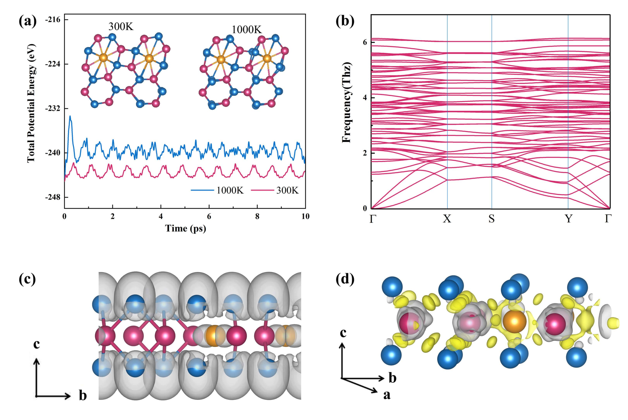
To estimate the feasibility of preparing these monolayers, the cleavage energies are calculated [Table I]. The calculated cleavage energy for X3YZ6 is between 0.44 and 0.63 J/m2, a little bigger than graphene (0.37 J/m2)graphite and much smaller than CaN2 (1.14 J/m2)can. The graphene have exfoliated successfully in experiment, monolayer X3YZ6 may expected to obtain in the same way. Moreover, we examine thermal stability of X3YZ6 by performing ab initio MD simulations. The average of the total potential energy stays the same after heating at 300 K for 10 ps [Fig. 2 (a) and supplementary material (SM) Fig. S1]. These results indicate clearly the materials remain thermal dynamically stable at room temperature. We also present the Ta3SnTe6 monolayer at 1000K and find the structure can still be maintained, so this monolayer has very high thermal stability and may be used to build nanoelectronic devices. The phonon spectra of Ta3SnTe6 and Ta3SiSe6 are plotted in Fig. 2 (b) and Fig. 6 (a) . The absence of imaginary mode in their spectra indicates dynamical stability. The single-layer X3YZ6 have very similar properties, so we mainly discuss Ta3SnTe6 and Ta3SiSe6 as examples.
We have plotted the electron localization function (ELF)elf with an isosurface of 0.78 in Fig. 2 (c). The ELF value is around 0.78 near Sn atoms and Te atoms, which means that electrons are more localized towards Sn and Te atoms. This type of electron localization indicates the ionic type of bonding between Ta and Sn (Te) atoms. To qualitatively analyze the charge transfer of Ta-Te (or Ta-Sn) bond, difference charge density map is plotted in Fig. 2 (d), the yellow/gray region represents charge accumulation/depletion, respectively. The difference pattern indicates the major charge transfer is from Ta atom to Te (or Sn) atom, which is consistent with the characteristics of an ionic bond. The similar results for Ta3SiSe6 and Ta3SiS6 are presented in Fig. S2.
| Structure | a(Å) | b(Å) | Ec(J/m2) | Structure | a(Å) | b(Å) | Ec(J/m2) |
|---|---|---|---|---|---|---|---|
| Ta3SiS6 | 5.825 | 10.851 | 0.53 | Nb3SiS6 | 5.835 | 10.961 | 0.46 |
| Ta3SiSe6 | 6.050 | 11.105 | 0.44 | Nb3SiSe6 | 6.069 | 11.210 | 0.44 |
| Ta3SiTe6 | 6.402 | 11.559 | 0.44 | Nb3SiTe6 | 6.410 | 11.634 | 0.63 |
| Ta3GeTe6 | 6.522 | 11.637 | 0.49 | Nb3GeTe6 | 6.536 | 11.706 | 0.50 |
| Ta3SnTe6 | 6.734 | 11.806 | 0.42 | Nb3SnTe6 | 6.745 | 11.880 | 0.50 |

Here, we have calculated the band structures and projected density of states (PDOS). In the absence of SOC, the Ta3SnTe6 displays a semimetal, the valence and conduction bands meet in the vicinity of the Fermi level and show a nodal line L1, as plotted in Fig. 3 (a). The energy of the nodal line L1 varies with 2 meV (flat) and it is not coexisting with other trivial bands (clean), making it an ideal NLSMs candidate materialshm. Moreover, there is a small band gap of 11 meV at high symmetry points Y labelled D2. The red line and point in the picture of the local gap near the Fermi level confirm the existence of L1 and D2, shown in Fig. 4 (a). Nodes and nodal lines are not confined to Fermi energy, but exist in a certain range near Fermi energy, which also appears in other topological semimetalsb1; b2. Additional band crossing are observed below the Fermi level in energy range of 0.5 eV, labelled two Dirac points D1, D3 and a nodal line L2b1; b2; b3. The obtained Fermi surfaces on the (001) cleaved surface are plotted in Fig. 4 (b), which is consistent with the previous analysis. In the middle, there are two long wavy lines around nodal line L1 and unsealed oval chain structure surrounding the D2. The band structures of the Ta3SiSe6 indicate it is also a semimetal in Fig. 3 (c), the nodal lines and nodes are similar to the case of Ta3SnTe6. The middle red line show the existing of nodal line L11 in Fig. 6 (b), but red point disappears because the band gap at point Y is larger, which leads to closed ellipse Fermi surface structure around it in Fig. 6 (c). The band structure diagrams of the remaining structures of X3YZ6 are shown in the Fig. S3, their electronic properties are more closer to case of Ta3SiSe6. To illustrate the unique electronic property, we have plotted the PDOS [Fig. 3 (a, c)], which agree well with the band structure distribution. The low-energy states around Fermi level are mainly from the Ta d orbitals, the contribution of Si (or Sn) and Se (or Te) p orbitals are very small.
To reveal the energy dispersion of the nodes and nodal lines, the 3D band structures of Ta3SnTe6 and Ta3SiSe6 are plotted in Fig. 5 (a, c, d) and Fig. 6 (d), respectively. The valence band maximum (VBM) and conduction band minimum (CBM) meet in the vicinity of Fermi level with opposite slopes, which shows type-Itype1; type2 nodal lines L1 and L11. The two bands form nodal line L2 with opposite slopes, so L2 is also a type-I nodal line. Although they are all type-I nodal lines, the shapes of the nodal lines are different. They are straight (L1), parabolic (L2) and curve (L11), respectively. The D1, D3 and D11 are type-II Dirac points, because the two bands are tilted in the same slope sign. The Berry phases around nodal line L1 and Dirac cone D1 are , further supporting the existence of the non-zero Berry phase and the existence of Dirac particles in Ta3SnTe6. The nodes and nodal lines near the Fermi surface has extremely high mobility, the Fermi velocity of D1 is anisotropic and about m/s in (010) surface, compared to HgTe quantum well ( m/s)vf.
The edge states are another manifestation of the nontrivial topological properties. The edge states of (010) and (110) surface for Ta3SnTe6 are showing in Fig. 4 (c, d). The corresponding positions of Dirac points and nodal line are found in the edge states. As an interesting feature of NLSMs is the appearance of flat band in the edge statesflat, we also find a flat band labelled with its band width being about 14 meV on the (110) surface edge state. Since the edges are electrically neutral, flat bands may be half-filled, providing an interesting platform for strongly correlated physicsflat. The edge states of Ta3SiSe6 are similar to the Ta3SnTe6’s, we also find the position of nodal line L11 and node D11 in the edge state, shown in Fig. 6 (e, f). The flat bands confirm the topological nontriviality of Ta3SnTe6 and Ta3SiSe6.


Then we discuss the stability of Dirac points and nodal lines under different cases. In the present of SOC, the X3YZ6 materials still display semimetal phases, the valence and conduction bands meet in the vicinity of the Fermi level [Fig. 3 (b, d) and Fig. S3]. For Ta3SnTe6, the nodal line L1 is gapped with a small band gap about 14 meV and form two Dirac points D4 and D5. The case of L2 is similar to L1, the nodal line becomes two Dirac points D6 and D7. The Fermi velocities are about m/s for D4 and m/s for D5 in X-S direction, which are close to case in Ta3SiTe6ta1. The band intersection P disappears, the band gap of D2 becomes small and forms a Dirac point. The 3D band structure around D2 shows the anisotropic Dirac cone [Fig. 5 (b)]. The Fermi velocity of D2 is about m/s in (010) surface. The zoom-in of the band structure around the X point and S point are plotted in Fig. 4 (e, f), the Dirac points become more obvious. The calculated edge states of the (010) and (110) surface are showing in Fig. 4 (g, h), which are another manifestation of the nontrivial topology of the Ta3SnTe6. One can see easily the emergence of topological nontrivial edge states and Dirac points. The changes of nodal lines for Ta3SiSe6 is similar to Ta3SnTe6’s, but the variation of band gap at the point Y is a little different. For Ta3SnTe6, the band gap at Y point becomes small and forms a Dirac point. But the band gap barely changes for Ta3SiSe6, there is no Dirac point. In fact, the X3YZ6 materials except Ta3SnTe6 have band gaps at point Y, only Ta3SnTe6 have an extra Dirac point D2.

To prove nodes and nodal lines are protected by symmetry, several tests are performed for Ta3SnTe6. First, we artificially shift the positions of the Ta atoms along the c axis to break the mirror symmetry Mz and maintain the . The node D1, nodal lines L1 and L2 are all fully gapped, while node D3 still exists, shown in Fig. 7 (c). These mean D1, L1 and L2 are protected by Mz symmetry in the absence of SOC. In the present SOC, the band of nodal line splits further to form two double degenerate points [Fig. 7 (e)]. Second, we shift the positions of the Ta atoms along the a axis to break the mirror symmetry and maintain the Mz symmetry. The nodes D1, D3, nodal lines L1 and L2 are all fully gapped in the absence of SOC, plotted in Fig. 7 (d), which means D1, L1 and L2 are protected by symmetry, while D3 and D2 are affected by . With considering SOC, the band splits further [Fig. 7 (f)]. To further clarify the relationship between D2 (or D3) and symmetry, we perform a third test. We use 10% uniaxial tensile strain along the a axis and b axis direction for single-layer Ta3SnTe6, but the crystal symmetry stays the same. The band structures are plotted in Fig. 7 (g) (h), we find the gaps of D1, L1 and L2 are not change, but the gap of D2 is changed and node D3 disappears under strain along the a axis, or the gap of D2 becomes zero and position of D3 has changed under strain along the b axis. These results show D1, L1 and L2 are protected by Mz and symmetry, D2 and D3 are affected by the two symmetries.

To test the effect of electron correlation on band structure, we perform GGA + U calculations with considering hubbard U correction of transition metal elements. Compared with GGA, there is little change in the results of single-layer Ta3SnTe6 and Ta3SiSe6, shown in Fig. S4 and S5. In addition, we use the hybrid functional HSE06 to check the electronic structure, similar nodes and nodal lines are found for single-layer Ta3SnTe6 and Ta3SiSe6 without considering the SOC in Fig. S6. We also have analyzed the electronic structure of the two-layer Ta3SnTe6 and found the nodes and nodal lines will still exist, as shown in Fig. S7.
IV. Conclusion
In summary, we find the monolayer X3YZ6 have similar properties and they are all TSMs materials based on the first principles calculations. The MD simulations indicate they are all thermal-dynamically stable. Taken Ta3SnTe6 and Ta3SiSe6 as examples, they have coexisting type-I nodal lines and type-II Dirac points in the absent of SOC. With the presence of SOC, the nodal lines become Dirac points and original Dirac points disappear. The characteristics of nodal lines and nodes can be clearly seen by using 3D band diagrams. Their nontrivial topological properties are confirmed by (010) and (110) surface edge states. The relationship among different nodal lines (nodes), crystal symmetry and SOC has been discussed. D1, L1 and L2 are protected by Mz and symmetry, D2 and D3 are affected by these two symmetries for Ta3SnTe6. The SOC cause the band to split further. X3YZ6 materials can be ideal candidates for the nodal line and node TSMs. These results can be used as a supplement to the research content of Ta3SiTe6 and provide theoretical basis for subsequent experimental research.
Acknowledgements.
This work was supported by National Natural Science Foundation of China (No. 11904312 and 11904313), the Project of Department of Education of Hebei Province, China(No. BJ2020015), and the Natural Science Foundation of Hebei Province (No. A2019203507 and A2020203027). The authors thank the High Performance Computing Center of Yanshan University.References
- (1) K. S. Novoselov, A. K. Geim, S. V. Morozov, D. Jiang, Y. Zhang, S. V. Dubonos, I. V. Grigorieva, and A. A. Firsov, Science 306, 666 (2004).
- (2) Y. Zhang, Y. W. Tan, H. L. Stormer, and P. Kim, Nature 438, 201 (2005).
- (3) Z. J. Wang, Y. Sun, X.Q. Chen, C. Franchini, G. Xu, H. Weng, X. Dai, and Z. Fang, Phys. Rev. B 85, 195320 (2012).
- (4) Z. Wang, H. Weng, Q. Wu, X. Dai, and Z. Fang, Phys. Rev. B 88, 125427 (2013).
- (5) S. M. Young, S. Zaheer, J. C. Y. Teo, C. L. Kane, E. J. Mele, and A. M. Rappe, Phys. Rev. Lett. 108, 140405 (2012).
- (6) H. M. Weng, C. Fang, Z. Fang, B. A. Bernevig, and X. Dai, Phys. Rev. X 5, 011029 (2015).
- (7) B.Q. Lv, H.M. Weng, B.B. Fu, X.P. Wang, H. Miao, J. Ma, P. Richard, X.C. Huang, L.X. Zhao, G.F. Chen, Z. Fang, X. Dai, T. Qian, and H. Ding, Phys. Rev. X 5, 031013 (2015).
- (8) A.A. Burkov, M.D. Hook, and L. Balents, Phys. Rev. B 84, 235126 (2011).
- (9) H. Weng, Y. Liang, Q. Xu, R. Yu, Z. Fang, X. Dai, and Y. Kawazoe, Phys. Rev. B 92, 045108 (2015).
- (10) K. Mullen, B. Uchoa, and D. T. Glatzhofer, Phys. Rev. Lett. 115, 026403 (2015).
- (11) C.J. Yi, B.Q. Lv, Q.S. Wu, B.B. Fu, X. Gao, and M. Yang, X.L. Peng, M. Li, Y.B. Huang, P. Richard, M. Shi, G. Li, O.V. Yazyev, Y.G. Shi, T. Qian, and H. Ding, Phys. Rev. B 97, 201107(R) (2018).
- (12) B. Bradlyn, J. Cano, Z. Wang, M. G. Vergniory, C. Felser, and R. J. Cava, Science 353, 6299 (2016).
- (13) Z. Zhu, G. W. Winkler, Q. S. Wu, J. Li, and A. A. Soluyanov, Phys. Rev. X 6, 031003 (2016).
- (14) H. M. Weng, C. Fang, Z. Fang, and X. Dai, Phys. Rev. B 94, 165201 (2016).
- (15) T. T. Heikkil and G. E. Volovik, New J. Phys. 17, 093019 (2015).
- (16) B. Q. Lv, Z. L. Feng, Q. N. Xu, X. Gao, and J. Z. Ma, Nature 546, 627 (2017).
- (17) Z. K. Liu, B. Zhou, Y. Zhang, Z. J. Wang, H. M. Weng, D. Prabhakaran, S. K. Mo, Z. X. Shen, Z. Fang, and X. Dai, Science 343, 864 (2014).
- (18) Z. K. Liu, J. Jiang, B. Zhou, Z. J. Wang, Y. Zhang, and H. M. Weng, Nat. Matter. 13, 677 (2014).
- (19) B. Lv, N. Xu, H. M. Weng, and J. Z. Ma, Nat. Phys. 11, 724 (2015).
- (20) X. Huang, L. Zhao, Y. Long, P. Wang, D. Chen, Z. Yang, H. Liang, M. Xue, H. Weng, Z. Fang, X. Dai, and G. Chen, Phys. Rev. X 5, 031023(2015).
- (21) S. Y. Xu, B. Ilya, A. Nasser, N. Madhab, B. Guang, and C. L. Zhang, Science 349, 613 (2015).
- (22) G. Bian, T. R. Chang, R. Sankar, S. Y. Xu, H. Zheng, T. Neupert, C. K. Chiu, and S. M. Huang, Nat. Commun. 7, 10556 (2016).
- (23) I. Belopolski, K. Manna, D. S. Sanchez, G. Q. Chang, and M. Z. Hasan, Science 365, 1278 (2019).
- (24) J. Hu, Z. J. Tang, J. Y. Liu, Y. L. Zhu, J. Wei, and Z. Q. Mao, Phys. Rev. B 96, 045127 (2017).
- (25) S. Y. Guan, P. J. Chen, M. W. Chu, R. Sankar, F. Chou, H. T. Jeng, C. S. Chang, and T. M. Chuang, Sci. Adv. 2, e1600894 (2016).
- (26) S. Ahn, E. J. Mele, and H. Min, Phys. Rev. Lett. 119, 147402 (2017).
- (27) S. Li, Y. Liu, S. S. Wang, Z. M. Yu, S. Guan, X. L. Sheng, Y. G. Yao, and S. Y. Yang, Phys. Rev. B 97, 045131 (2018).
- (28) T. Sato, Z. Wang, K. Nakayama, S. Souma, D. Takane, Y. Nakata, H. Iwasawa, C. Cacho, T. Kim, T. Takahashi, and Y. Ando, Phys. Rev. B 98, 121111(R) (2018).
- (29) L. L. An, H. Zhang, J. Hu, X. D. Zhu, W. S. Gao, J. L. Zhang, C. Y. Xi, W. Ning, Z. Q. Mao, and M. L. Tian, Phys. Rev. B 97, 235133 (2018).
- (30) M. Naveed, F. C. Fei, H. J. Bu, X. Y. Bo, S. A. Shah, B. Chen, Y. Zhang, Q. Q. Liu, B. Y.Wei, S. Zhang, J. W. Guo, C. Y. Xi, A. Rahman, Z. M. Zhang, M. H. Zhang, X. G. Wan, and F. Q. Song, Appl. Phys. Lett. 116, 92402 (2020).
- (31) Q. Wan, T.Y. Yang, S. Li, M. Yang, Z. Zhu, C.L. Wu, C. Peng, S.K. Mo, W. Wu, Z.H. Chen, Y.B. Huang, L.L. Lev, V. N. Strocov, J. Hu, Z.Q. Mao, H. Zheng, J.F. Jia, Y.G. Shi, S.A. Yang, and N. Xu, Phys. Rev. B 103, 165107 (2021).
- (32) S. Roy, R. Singha, A. Ghosh, and P. Mandal, Phys. Rev. Mater. 5, 064203 (2021).
- (33) X. T. Wang, G. Q. Ding, S. Khandy, Z. Cheng, G. Zhang, X. L. Wang, and H. Chen, Nanoscale 12, 16910 (2020).
- (34) K. S. Novoselov, D. Jiang, F. Schedin, T. J. Booth, and V. V. Khotkevich, Proc. Natl. Acad. Sci. 102, 10451 (2005).
- (35) J. Hu, X. Liu, C. L. Yue, J. Y. Liu, H. W. Zhu, J. B. He, J. Wei, Z. Q. Mao, L. Y. Antipina, Z. I. Popov, P. B. Sorokin, T. J. Liu, P.W. Adams, S. M. A. Radmanesh, L. Spinu, H. Ji, and D. Natelson, Nat. Phys. 11, 471 (2015).
- (36) G. Kresse and J. Furthmuller, Phys. Rev. B 54, 11169 (1996).
- (37) G. Kresse and J. Furthmuller, Comput. Mater. Sci. 6, 15 (1996).
- (38) J.P. Perdew and J. A. Chevary, S.H. Vosko, K.A. Jackson, M.R. Pederson, D.J. Singh, and C. Fiolhais, Phys. Rev. B 46, 6671 (1992).
- (39) J.P. Perdew, K. Burke, and M. Ernzerhof, Phys. Rev. Lett. 77, 3865 (1996).
- (40) H. J. Monkhorst and J. D. Pack, Phys. Rev. B 13, 5188 (1976).
- (41) J. Heyd, G. E. Scuseria, and M. Ernzerhof, J. Chem. Phys. 118, 8207 (2006).
- (42) N. Marzari and D. Vanderbilt, Phys. Rev. B 56, 12847 (1997).
- (43) I. Souza, N. Marzari, D. Vanderbilt, Phys. Rev. B 65, 035109 (2001).
- (44) Q. Wu, S. Zhang, and H. F. Song, Comput. Phys. Commun. 224, 405 (2018).
- (45) S. Baroni, S. D. Gironcoli, A. D. Corso, and P. Giannozzi, Rev. Mod. Phys. 73, 515 (2001).
- (46) R. Zacharia, H. Ulbricht, and T. Hertel, Phys. Rev. B 69, 155406 (2004).
- (47) S. Zhao, Z. Li, and J. Yang, J. Am. Chem. Soc. 136, 13313 (2014).
- (48) A. Savin, R. Nesper, S. Wengert, and T. F. Fassler, Angew. Chem. Int. Ed. Engl. 36, 1808 (1997).
- (49) R.W. Zhang, X. D. Zhou, Z. Y. Zhang, D. S. Ma, Z. M. Yu, W. X. Feng, and Y. G. Yao, Nano Lett. 21, 8749 (2021).
- (50) B.S. Wang, H. Gao, Q. Lu, W. H. Xie, Y. F. Ge, Y. H. Zhao, K. C. Zhang, and Y. Liu, Phys. Rev. B 98, 115164 (2018).
- (51) Y.L. Jiao, F. X. Ma, C. M. Zhang, J. Bell, S. Sanvito, and A. J. Du, Phys. Rev. Lett. 119, 016403 (2017).
- (52) P. Zhou, Z. Ma, and L. Sun, J. Mater. Chem. C 6, 1206 (2018).
- (53) S. Li, Z.M. Yu, Y. Liu, S. Guan, S.S. Wang, X. Zhang, Y. Yao, and S.A. Yang, Phys. Rev. B 96, 081106(R) (2017).
- (54) X. Zhang, L. Jin, X. Dai, and G. Liu, J. Phys. Chem. Lett. 8, 4814 (2017).
- (55) Y. Xu, B. Yan, H.J. Zhang, J.Wang, G. Xu, P. Tang, W. Duan, and S.C. Zhang, Phys. Rev. Lett. 111, 136804 (2013).
- (56) B. Yang, X. M. Zhang, and M. W. Zhao, Nanoscale 9, 8740 (2017).