跳到论文正文
W Papers独立论文阅读器 arXiv:2201.11649 论文正文 计算阅读时间 · 0%
引用这篇论文根据当前论文元数据生成,正式投稿前建议核对。


License: arXiv.org perpetual non-exclusive license
arXiv:2201.11649v1 [math.OC] 26 Jan 2022
\addtokomafont

captionlabel \titleheadMaster Thesis 35 \publishers Prüfer: Prof. Dr. Frank Allgöwer Betreuer: Msc. Catalin Arghir Prof. Dr. Florian Dörfler
Institut für Systemtheorie und Regelungstechnik
Universität Stuttgart
Prof. Dr.-Ing. Frank Allgöwer \KOMAoptionstwoside=false \recalctypearea

Grid-friendly Matching Control of Synchronous Machines by DC/AC Converters in Bulk Power Networks

Taouba Jouini
June 7, 2016
\KOMAoptions

twoside=true \recalctypearea

An islanded inverter-based microgrid is a collection of heterogeneous DC energy resources, e.g., photovoltaic arrays, fuel cells, and energy-storage devices, interfaced to an AC distribution network and operated independently from the bulk power system. Energy conversion is typically managed by power-electronics in voltage source inverters. Drawing from the control of synchronous machines in bulk power systems, different control schemes have been recently adopted in order to achieve a stable network operation. The vast majority of academic and industrial efforts opt for these strategies during real-time operation.

Starting with a dynamical averaged DC/AC converter model, we review different controllers by presenting its main scope analytically and through simulations. Next, we explore a new alternative of controlling DC/AC converters in bulk power systems by matching traditional synchronous machines with emphasis on the role that DC-circuit can play in control architecture, usually neglected in conventional strategies. Compared to standard emulation methods, our controller relies solely on readily available DC-side measurements and takes into account the natural DC and AC storage elements. As a result, our controller is generally faster and less vulnerable to delays and measurement inaccuracies. We additionally provide insightful interpretations of the suggested control, various plug-and-play properties of the closed loop, such as steady-state power flow analysis, passivity with respect to the DC and AC ports, stability proof as well as high-level control architectures contributing to enhancing the controller performance and attaining further control goals, which we illustrate in both analysis and simulation.

Ein Inselnetz fähiges Microgrid ist eine Sammlung von heterogenen DC- Energiequellen, beispielsweise Photovoltaik Anlagen, Brennstoffzellen und Energiespeicher, die mit einem AC Verteilungsnetz angeschlossen und unabhängig vom Hauptstromsystem betrieben sind. Energieumwandlung wird in der Regel von Leistungselektronik in Spannungszwischenkreisumrichter verwaltet. Aufbauend auf die Konzepte der Regelung von Synchronmaschinen in Großstromanlagen sind letztlich unterschiedliche Schemata angenommen um einen stabilen Netzbetrieb zu erreichen. Die überwiegende Mehrheit der akademischen und industriellen Anstrengungen entscheiden sich für diese Strategien während der Echtzeit-Regelung von DC/AC Wandlern.

Beginnend mit einem dynamischen gemittelten DC/AC- Wandler Modell, führen wir die Grundgedanken verschiedener Regelungsstrategien ein und prüfen die Umsetzbarkeit ihrer Regelungsvorschriften analytisch und durch Simulationen. Als Nächstes erkunden wir eine neue Alternative zur Regelung von DC/AC- Wandler in Stromanlagen durch Anpassung an einem entsprechenden hochdimensionalen Synchronmaschinen Modell mit dem Schwerpunkt aufgesetzt auf die Rolle, die die Gleichstromschaltung in Regelungsarchitektur spielen kann, was in der Regel in konventionellen Strategien vernachlässigt wird. Im Vergleich zu den standardisierten Verfahren stützt sich unser Regler ausschließlich auf leicht verfügbaren Messungen von der DC-Seite und berücksichtigt dabei die natürliche Gleich- und Wechselspeicherelemente vorhanden in einem DC/AC Wandler. Als Ergebnis ist unser Regler im allgemeinen schneller und weniger anfällig zu Verzögerungen und Messungenauigkeiten. Wir bieten zusätzlich interessante Interpretationen der vorgeschlagenen Regelung, verschiedene Plug-und-Play Eigenschaften im geschlossenen Kreis durch stationäre Leistungsflussanalyse, Passivität gegenüber DC- und AC inputs, Stabilitätsbeweis sowie höhere Stufen für eine erweiterte Regelung, um die Leistung des DC/AC Wandlers zu verbessern und andere Ziele zu erreichen, die wir sowohl in Analyse als auch in Simulation darstellen.

Chapter 0 Introduction

[Uncaptioned image]

The history of electric power systems began with the inventors Nicola Tesla (1856−1943)(1856-1943) and Thomas Edison (1847−1931)(1847-1931) who contributed to the development of electric power systems that are widely used today. Tesla and Edison set the basis for most of AC and DC machinery.

In conventional bulk power plants, synchronous machines (SM) dominate. In fact, rotating generators are electro-mechanical converters. The interaction between the mechanical interface and the electrical port is described by the following equation

M​dd​t​ω​(t)=Pgeneration​(t)−Pdemand​(t);{M\,\frac{d}{dt}\,\omega(t)\;=\;{P}_{\textup{generation}}(t)-{P}_{\textup{demand}}(t)}\,\mathchar 59\relax

where M=ω​J\omega J, ω\omega is AC frequency and JJ is the moment of inertia. This implies that a change in the kinetic energy is the instantaneous power balance between the generation and the demand.

[Uncaptioned image]

In classical power system, SMs offer favorable features to support system operation. Indeed SMs contribute to the system damping through their inertia and participate in the primary frequency regulation as the frequency response, depicted in Figure 1 found in most of power systems literature. The rotor mass MM stabilizes the system by providing damping contributing to the enhancement of system performance. As a matter of fact, synchronous machine dynamics describe a natural differential controller for the frequency ω\omega with the D-gain MM.

Figure 1: Frequency response of a synchronous machine after a disturbance at t=5t=5s

The advantageous capabilities are not inherently offered by power electronics interfaces commonly adopted for the integration of renewable energy. In other words, the increase of small-scale dispersed power generation is likely to impact the structure and operation of power systems. As a matter of fact, power systems are increasingly based on non-rotational generation with power electronic converters interfacing renewable energy storage and batteries with the AC power grid. A major challenge in such low-inertia networks is the replacement of stabilizing rotational inertia of SMs and their ancillary services through control of converters [27]. The so-called grid-forming converter control strategies range from droop methods, emulation of synchronous machines to more general limit-cycle oscillator based strategies. This name is attributed to the power electronic converters since they have the capability to connect to a DC and AC grid sides. These control schemes are often brand-marked as grid-friendly since they are based on fully decentralized control, naturally backward compatible with SM, and ultimately increase system inertia.

For its correct operation, electric power systems must satisfy a large set of different regulation objectives, that are typically associated to multiple time-scale behaviors of the system. A hierarchal architecture usually serves as nested control loop in order to operate at different time scales as shown in Figure 2, where the curves describe an overlap of the frequency behavior in Mettlen, Switzerland and that of Athens according to control intervention after disturbances. Primary control is of fundamental importance, when perturbation occurs. Its main objective consists in adjusting promptly the reference to be provided to the inner-loop, consisting in the innermost cascaded control interfaced with the DC/AC converter model and aiming to track a given reference by the primary control. Primary control maintains stability according to a pre-specified power distribution called also power sharing. It operates in the time scale of m​sms. Secondary control calculates mainly current and voltage references or recalculates power references derived from higher-level control called tertiary control. The latter is the outermost level of control. It is usually based on optimization algorithms of power flow which generate nominal or perturbed reference associated with the appropriate operating conditions. The time required for intervention of tertiary control ranges from 2020 min to 11 h.

Refer to caption
Figure 2: Frequency response of synchronous machine following up a system disturbance according to a predefined hierarchical control architecture.

Bearing in mind all the difficulties imposed by conventional control architecture and the challenges arising after retirement of synchronous machines, we propose in this thesis a novel strategy of controlling converters compensating for the absence of SMs and assuring a stable network operation. Starting from a model showing attention to the DC-side available in a converter and a high-order model of SM taking into account both rotor and stator dynamics, we find a controller that matches the two models by comparing rotor dynamics to that of a DC circuit. Compared to virtual synchronous machine and emulation algorithms, we use matching rather than virtual emulation due to the involvement of the physical storage rather than the virtual storage element commonly used to replace the mechanical inertia of a SM and rooted in a structural similarity, i.e an equivalence between the two models up to a defined order (in per unit). Towards a generalization for a network consisting of multiple identical converters connected to a grid, our control scheme fulfills certain primary control goals. These promising properties range from inducing droop behavior serving as a typical control requirement and preserving passivity in closed-loop to assuring stability in closed loop fashion. High-order loops can be constructed and added to the matching control by taking into account different objectives in order to keep currents and voltages within limits and track a desired frequency. Our predictions for the network case are validated through simulations which establishes the basis towards assuring power sharing between multiple converters.

The remainder of this work is organized as follows, Section 1 presents an averaged three-phase DC/AC converter model. Based on it, we review in Section 2 conventional control schemes, described by the innermost control loops called inner-loop control as well as outer-loops ranging from droop, oscillation-based to virtual synchronous machine methods. Section 3 presents the main analogies between SM and DC/AC converter model and proposes an intuitive control strategy to match them based on a structural equivalence between the two models. Section 4 deals with the properties of the closed-loop DC/AC converter and highlights its plug-and-play characteristics at steady state including power flow analysis, synchronization for AC signals and passivity with respect to the DC and AC grid inputs. In Section 5, a proof of the global asymptotic stability of the desired equilibrium set is derived using Lyapunov theory. We provide further extensions of this novel control strategy in Section 6, where one may notice the flexibility of our control design, since it can be extended through its gains by outer loops measuring DC and AC sides and achieving further control goals. Finally, we provide simulations of the multiple DC/AC converters case once connected to the grid in Section 7. Our observations open up horizons of further investigating the proposed approach as a decentralized control in a grid network by enhancing its performance in terms of frequency regulation and power sharing from a networked viewpoint.

Chapter 1 Modeling of a three-phase inverter

In this chapter, we introduce the usual working frame of the three-phase alternating current (AC) signals in electric power as well as the background necessary to assimilate the transformations performed from one domain to the other and required for different analysis purposes in the remainder of this work. Next, we introduce the averaged model of a DC/AC converter serving as basis for our future investigations.

1 Background

1 Three-phase signals

A 33-phase AC signal represented in (abc) frame is a vector in za​b​c∈3z_{abc}\in\real^{3} defined by its amplitude z^\hat{z} and angles at each phase (a)(a), (b)(b) or (c)(c) with the phase angle difference of 2​π/3{2\pi}/{3} defined as follows

za​b​c=z^​[sin⁡(θ)sin⁡(θ−2​π3)sin⁡(θ+2​π3)]​;​z^>0z_{abc}=\hat{z}\begin{bmatrix}\sin(\theta)\\ \sin(\theta-\frac{2\pi}{3})\\ \sin(\theta+\frac{2\pi}{3})\end{bmatrix}\mathord{\mathchar 59\relax}\,\hat{z}>0 (1)

When the angle difference is exactly of 2​π/32\pi/3, the signal is considered to be balanced such that it holds

za+zb+zc=1⊤​za​b​c=0z_{a}+z_{b}+z_{c}=1^{\top}z_{abc}=0 (2)

as shown in the Figure 1.

Refer to caption
Figure 1: Representation of balanced three phase-signal in the phasor plane and in time-domain

If the condition (2) is violated, the three-phase AC signal is considered to be unbalanced

2 Clarke transformation to (α​β)(\alpha\beta) frame

Assuming a balanced three-phase signal za​b​c∈3z_{abc}\in\real^{3}, i.e 1⊤​za​b​c=01^{\top}z_{abc}=0, we can represent AC signals in (α​β)(\alpha\beta)- frame, where we can omit one component and take zα​β∈2z_{\alpha\beta}\in\real^{2}. We can perform a change of coordinates from (a​b​c)(abc) domain into (α​β)(\alpha\beta) domain using Tα​β:ℝ3→ℝ3T_{\alpha\beta}:\mathbb{R}^{3}\to\mathbb{R}^{3} defined as follows:

Tα​β=23​[1−12−12032−32121212]T_{\alpha\beta}=\sqrt{\frac{2}{3}}\begin{bmatrix}1&\frac{-1}{2}&\frac{-1}{2}\\ 0&\frac{\sqrt{3}}{2}&-\frac{\sqrt{3}}{2}\\ \frac{1}{\sqrt{2}}&\frac{1}{\sqrt{2}}&\frac{1}{\sqrt{2}}\end{bmatrix} (3)

with the inverse Tα​β−1=Tα​β⊤T_{\alpha\beta}^{-1}=T_{\alpha\beta}^{\top}. An advantage of the choice of the matrix Tα​βT_{\alpha\beta} is the easy inverse and invariance power calculation, where the power in (α​β)(\alpha\beta)- frame is the same as in (a​b​c)(abc)- frame, i.e power calculation does not require a scaling factor. After transformation into (α​β)(\alpha\beta)- frame

zα​β\displaystyle z_{\alpha\beta} =Tα​β​za​b​c=z^​32​[−sin⁡(θ)cos⁡((θ)CLOSE0]\displaystyle=T_{\alpha\beta}z_{abc}=\hat{z}\sqrt{\frac{3}{2}}\begin{bmatrix}-\sin(\theta)\\ \cos((\theta)\\ 0\end{bmatrix} (4a)
d​zα​βd​θ\displaystyle\,\frac{dz_{\alpha\beta}}{d\theta} =Tα​β​d​za​b​cd​θ=z^​32​[cos⁡(θ)sin⁡(θ)0]=J3​zα​β;\displaystyle=T_{\alpha\beta}\frac{dz_{abc}}{d\theta}=\hat{z}\sqrt{\frac{3}{2}}\begin{bmatrix}\cos(\theta)\\ \sin(\theta)\\ 0\end{bmatrix}=J_{3}z_{\alpha\beta}\,\mathchar 59\relax (4b)

with J3=[0−10100000]J_{3}=\begin{bmatrix}0&-1&0\\ 1&0&0\\ 0&0&0\end{bmatrix}.

Refer to caption
Figure 2: Three-phase and two-phase stationary reference frames[29]

This coordinate change can be interpreted as a projection from a sphere in 𝕊3\mathbb{S}^{3} of radius z^>0\hat{z}>0 into a circle of radius z^​3/2>0\hat{z}\sqrt{{3}/{2}}>0 in 2, where the derivative of a vector with respect to the angle θ\theta, is the same as a rotation with angle π/2{\pi}/{2} of the same vector in (α​β)(\alpha\beta)-frame.

In fact, (α​β)(\alpha\beta)- transformation can be understood as that of a natural polar coordinate representation of the three-phase AC signals za​b​c∈3z_{abc}\in\real^{3}, since it allows to represent a vector by its amplitude z^​3/2>0\hat{z}\sqrt{{3}/{2}}>0 and its angle θ∈𝕊\theta\in\mathbb{S} as zα​β∈2z_{\alpha\beta}\in\real^{2} such that

zα​β=z^​32​[−sin⁡(θ)cos⁡(θ)]=Tα​β​za​b​c.z_{\alpha\beta}=\hat{z}\sqrt{\frac{3}{2}}\begin{bmatrix}-\sin(\theta)\\ \cos(\theta)\end{bmatrix}=T_{\alpha\beta}z_{abc}\,.
Remark 1 (Complex form).

Any vector in (α​β)(\alpha\beta) coordinates can be represented by a complex number z→α​β∈ℂ\vec{z}_{\alpha\beta}\in\mathbb{C}

z→α​β=zα+j​zβ;\vec{z}_{\alpha\beta}=z_{\alpha}+jz_{\beta}\,\mathchar 59\relax (5)

where j=−1j=\sqrt{-1}.

3 Park transformation to rotating d​q​0dq0 domain

Steady state currents and voltages for the (a​b​c)(abc) phases of a single generator are sinusoidal waveforms. There exists a transformation of the (a​b​c)(abc) phases to the (d​q​0)(dq0) frame using Td​q​0:ℝ3→ℝ3T_{dq0}:\mathbb{R}^{3}\to\mathbb{R}^{3} defined as follows:

Td​q​0​(γ)=23​[cos⁡(γ)cos⁡(γ−2​π3)cos⁡(γ+2​π3)sin⁡(γ)sin⁡(γ−2​π3)sin⁡(γ+2​π3)121212]=R−γ​Tα​β;T_{dq0}(\gamma)=\sqrt{\frac{2}{3}}\begin{bmatrix}\cos(\gamma)&\cos(\gamma-\frac{2\pi}{3})&\cos(\gamma+\frac{2\pi}{3})\\ \sin(\gamma)&\sin(\gamma-\frac{2\pi}{3})&\sin(\gamma+\frac{2\pi}{3})\\ \frac{1}{\sqrt{2}}&\frac{1}{\sqrt{2}}&\frac{1}{\sqrt{2}}\end{bmatrix}=R_{-\gamma}\,T_{\alpha\beta}\,\mathchar 59\relax (6)

with the inverse Td​q​0−1=Td​q​0⊤T_{dq0}^{-1}=T_{dq0}^{\top} and Tα​βT_{\alpha\beta} corresponding to the transformation matrix to the power invariant formulation from (a​b​c)(abc) to (α​β)(\alpha\beta)- frame defined in (3) and RγR_{\gamma} is the rotation matrix defined as follows

R−γ=[cos⁡(γ)sin⁡(γ)0−sin⁡(γ)cos⁡(γ)0001].R_{-\gamma}=\begin{bmatrix}\cos(\gamma)&\sin(\gamma)&0\\ -\sin(\gamma)&\cos(\gamma)&0\\ 0&0&1\end{bmatrix}\,.

We can therefore map (a​b​c)(abc)- currents and voltages to (d​q​0)(dq0) domain using (6)

zd​q​0=(zd,zq,z0)=Td​q​0​(za,zb,zc).z_{dq0}=(z_{d}\mathchar 59\relax z_{q}\mathchar 59\relax z_{0})=T_{dq0}\,(z_{a}\mathchar 59\relax z_{b}\mathchar 59\relax z_{c})\,. (7)

It is noteworthy that a transformation from (d​q​0)(dq0) into (α​β)(\alpha\beta)- frame, is a rotation of angle γ\gamma, defined as follows

zα​β=Rγ​zd​q​0;z_{\alpha\beta}=R_{\gamma}z_{dq0}\,\mathchar 59\relax

with Rγ=R−γ⊤R_{\gamma}=R_{-\gamma}^{\top}.
We now consider the vector za​b​cz_{abc} as defined previously in (1)

zd​q​0=Td​q​0​(γ)​za​b​c​(θ)=z^​32​[sin⁡(θ−γ)cos⁡(θ−γ)0].z_{dq0}=T_{dq0}(\gamma)z_{abc}(\theta)=\hat{z}\sqrt{\frac{3}{2}}\begin{bmatrix}\sin(\theta-\gamma)\\ \cos(\theta-\gamma)\\ 0\end{bmatrix}\,.

A transformation of a balanced three-phase vector in (a​b​c)(abc) into (d​q​0)(dq0) frame defines a projection to a vector rotating with angle γ\gamma living on a circle with radius z^​3/2\hat{z}\sqrt{{3}/{2}}. If we additionally choose the angle of the transformation matrix Td​q​0T_{dq0} to be the angle of the balanced three-phase vector γ=θ\gamma=\theta, it yields

zd​q​0=Td​q​0​(θ)​za​b​c​(θ)=z^​32​[010];z_{dq0}=T_{dq0}(\theta)z_{abc}(\theta)=\hat{z}\sqrt{\frac{3}{2}}\begin{bmatrix}0\\ 1\\ 0\end{bmatrix}\,\mathchar 59\relax

which defines a projection from a point on a sphere in ℝ3\mathbb{R}^{3} into a point in ℝ\mathbb{R} as shown in Figure 3.

Refer to caption
Figure 3: Three-phase and two-phase rotating reference frame d​q​0dq0 with frequency ω\omega[29]

Assuming a balanced system, we ignore the zero component and take zd​q∈2z_{dq}\in\real^{2}.

Definition 1.1 (Equilibria in the (d​q​0)(dq0)- frame).

We assume that at steady state AC signals exhibit harmonics synchronous at ωs\omega_{s} in the (d​q​0)(dq0)- frame with θ˙=γ˙=ωs\dot{\theta}=\dot{\gamma}=\omega_{s} and we consider its dynamics in (d​q​0)(dq0)- frame, where we use the fact that J2​Td​q​(γ)=Td​q​(γ)​J2J_{2}T_{dq}(\gamma)=T_{dq}(\gamma)J_{2} to get

z˙d​q\displaystyle\dot{z}_{dq} =T˙d​q​(γ)​zα​β+Td​q​(γ)​z˙α​β\displaystyle=\dot{T}_{dq}(\gamma)z_{\alpha\beta}+T_{dq}(\gamma)\dot{z}_{\alpha\beta}
=−J2​ωs​Td​q​(γ)​zα​β+J2​ωs​Td​q​(γ)​zα​β\displaystyle=-J_{2}\omega_{s}T_{dq}(\gamma)z_{\alpha\beta}+J_{2}\omega_{s}T_{dq}(\gamma)z_{\alpha\beta}
=−ωs​J2​zd​q+ωs​J2​zd​q\displaystyle=-\omega_{s}J_{2}z_{dq}+\omega_{s}J_{2}z_{dq}
=0;\displaystyle=0\,\mathchar 59\relax

Therefore, an equilibrium in (d​q)(dq)- frame describes a point in 2.

4 Power calculation

Definition 1.2 (Instantaneous AC Power).

We define the active and reactive power flowing out of an AC voltage node uα​βu_{\alpha\beta} on an edge defined by an AC current yα​βy_{\alpha\beta} as

Pu\displaystyle P_{u} =uα​β⊤​yα​β\displaystyle=u_{\alpha\beta}^{\top}\,y_{\alpha\beta}
Qu\displaystyle Q_{u} =uα​β⊤​[0−110]​yα​β.\displaystyle=u_{\alpha\beta}^{\top}\begin{bmatrix}0&-1\\ 1&0\end{bmatrix}y_{\alpha\beta}\,.

This definition is in accordance with Akagi’s instantaneous power theory [18].

Instantaneous active and reactive power can be rewritten (α​β)(\alpha\beta) frame as follows:

[PQ]=[vαvβvβ−vα]​[iαiβ];\begin{bmatrix}P\\ Q\end{bmatrix}=\begin{bmatrix}v_{\alpha}&v_{\beta}\\ v_{\beta}&-v_{\alpha}\end{bmatrix}\begin{bmatrix}i_{\alpha}\\ i_{\beta}\end{bmatrix}\,\mathchar 59\relax (10)

where vv and ii are the voltage and current measured at the same node.

Complex form

Instantaneous power expressions can be derived from the complex power S→\vec{S} defined as follows:

S→=v→α​β​i→α​β∗=(vα​iα+vβ​iβ)⏟P+j​(−vα​iβ+vβ​iα)⏟Q;\vec{S}={\vec{v}_{\alpha\beta}}\vec{i}_{\alpha\beta}^{*}=\underbrace{(v_{\alpha}i_{\alpha}+v_{\beta}i_{\beta})}_{P}+j\underbrace{(-v_{\alpha}i_{\beta}+v_{\beta}i_{\alpha})}_{Q}\,\mathchar 59\relax

where j=−1j=\sqrt{-1} and * is the complex conjugate of a complex number.

5 Modeling principles in power systems

Any wire can be modeled as inductance. If it is lossy, a resistor is put in series connection to the inductance. Therefore, we model a wire as an RL circuit. The earth acts as a ground and justifies the usage of the capacitors. Since the transmission lines are usually very long, there exists a capacitance with respect to the earth. They are modeled as shunt capacitors. A shunt is in general an endpoint connected to an element which is extended in this context to the ground.

We design by terminals, the endpoint of an electrical component. In the case of a DC/AC converter model, its terminals correspond additionally to a connection point to the grid.

Averaging of DC/AC converter

An averaged value of an AC quantity x⁡(t)x(t) over a period TsT_{s} is defined by

x¯=1Ts​∫t−Tstx⁡(τ)​𝑑τ\bar{x}=\frac{1}{T_{s}}\int_{t-T_{s}}^{t}x(\tau)d\tau (11)

We extensively use, in the derivation of the dynamic controlled models of the several converters, the fundamental Kirchoff’s current and Kirchoff’s voltage laws. The methodology for the derivation of the models is therefore, quite straightforward. We fix the position of the switch, or switches, and derive the differential equations of the circuit model. We then combine the derived models into a single one parameterized by the switch position function whose value must coincide, for each possible case, with the numerical values of either “zero” or “one”. In other words, the numerical values ascribed to the switch position function is the binary set {0;1}\{0\mathchar 59\relax 1\}. The obtained switched model is then interpreted as an average model by letting the switch position function take values on the closed interval of the real line [0​;​1][0\mathord{\mathchar 59\relax}1]. This state averaging procedure has been extensively justified in the literature since the early days of power electronics and, therefore, we do not dwell into the theoretical justifications of such averaging procedure [30].

The request for a certain load voltage is translated into a corresponding requirement for the converter duty cycle. The duty cycle modulation is typically several orders of magnitude slower than the switching frequency. The net effect is attainment of an average voltage with relatively small ripples. See Figure 4 for a zoomed-in view of this dynamics.

Refer to caption
Figure 4: converter output voltage generation (source: internet)

2 The averaged converter model

Assumption 2.1 (AC Signals).

All 33-phase AC quantities, i.e. za​b​c∈3z_{abc}\in\real^{3}, are considered to be balanced in (a​b​c)(abc)- frame. We denote by zα​β∈2z_{\alpha\beta}\in\real^{2} the representation in (α​β)(\alpha\beta)- domain and omit the third component, denoted by zγ∈z_{\gamma}\in\real.

In this section, we consider an averaged model of a 33-phase converter composed of a linear DC circuit, a linear AC circuit and a nonlinear modulation block. The diagram in Figure 5 depicts the model of a three-phase inverter described in (a​b​c)(abc)- frame as follows [12]

il​o​a​di_{load}++−\vphantom{+}-vx{v}_{x}ia​b​ci_{abc}RRLLCC−\vphantom{+}-++va​b​cv_{abc}id​ci_{dc}Gd​cG_{dc}Cd​cC_{dc}ixi_{x}−\vphantom{+}-++vd​c{v}_{dc}
Figure 5: Circuit diagram of a three-phase DC/AC converter
  • •

    The DC circuit is represented by a constant current source id​c>0i_{dc}>0, in parallel to a capacitance Cd​c>0C_{dc}>0 and a conductance Gd​c>0G_{dc}>0. Furthermore ixi_{x} is the current at the output of the DC circuit and vd​cv_{dc}, the voltage across the DC capacitance. We can write the DC model equation as

    Cd​c​v˙d​c=−Gd​c​vd​c+id​c−ix.C_{dc}\dot{v}_{dc}=-G_{dc}v_{dc}+i_{dc}-i_{x}\,. (12)
  • •

    The AC circuit contains at each phase an inductance L>0L>0 in series with a resistance R>0R>0 connected to a shunt capacitance C>0C>0 to ground. Here va​b​cv_{abc} is the AC voltage across the capacitor, il​o​a​di_{load} is the AC current drawn by the external load, ia​b​ci_{abc} is the AC current in the inductance and vxv_{x} the average AC voltage at the output of the modulation block. The dynamic of the linear AC circuit can be captured in (a​b​c)(abc)- frame by the following equations:

    C​v˙a​b​c\displaystyle C\,\dot{v}_{abc} =−il​o​a​d+ia​b​c\displaystyle=-i_{load}+i_{abc} (13a)
    L​(ia​b​c)˙\displaystyle\,L\dot{(i_{abc})} =−R​ia​b​c+vx−va​b​c;\displaystyle=-Ri_{abc}+v_{x}-v_{abc}\,\mathchar 59\relax (13b)

    where va​b​cv_{abc} is the capacitor terminal voltage, il​o​a​di_{load} is the current drawn by the grid load, ia​b​ci_{abc} is the inductance current and vxv_{x} the terminal voltage at the modulation output block.

  • •

    The switching block represents an averaged model of a 66-switch, 22-level inverter which modulates DC voltage into AC voltage according to a complementary switching pattern and a modulation signal ma​b​cm_{abc}. For the time scale of interest, we assume a high enough switching frequency which allows us to discard all switching harmonics (no ripples). This block represents the main nonlinearity in our system and is defined using the following identities, as in [12]:

    ix=12​ma​b​c⊤​ia​b​c;vx=12​ma​b​c​vd​c;i_{x}=\frac{1}{2}m_{abc}^{\top}i_{abc}\,\mathchar 59\relax v_{x}=\frac{1}{2}m_{abc}v_{dc}\,\mathchar 59\relax

    with ma​b​c∈3m_{abc}\in\real^{3} as the modulation signal in (a​b​c)(abc)-frame, corresponding to the average of the converter duty cycle over one switching period and therefore its components take values in [−1​;​1][-1\mathord{\mathchar 59\relax}1]. The modulation signal will serve as our main control input later on.

By combining (13) and (13b), we can rewrite the three-phase inverter model equations in (a​b​c)(abc)- frame as:

Cd​c​v˙d​c\displaystyle C_{dc}\dot{v}_{dc} =−Gd​c​vd​c+id​c−12​ma​b​c⊤​ia​b​c\displaystyle=-G_{dc}v_{dc}+i_{dc}-\frac{1}{2}m_{abc}^{\top}i_{abc}
C​v˙a​b​c\displaystyle\,C\dot{v}_{abc} =−il​o​a​d+ia​b​c\displaystyle=-i_{load}+i_{abc}
L​(ia​b​c)˙\displaystyle\,L\dot{(i_{abc})} =−R​ia​b​c+12​ma​b​c​vd​c−va​b​c;\displaystyle=-Ri_{abc}+\frac{1}{2}m_{abc}v_{dc}-v_{abc}\,\mathchar 59\relax

where all quantities are averaged over one switching cycle.
We refer to all quantities in the AC circuit as vectors in ℝ3\mathbb{R}^{3} with three elements, each describing a phase in the (a​b​c)(abc)- frame, whereas DC quantities are considered to be real.

Representation of the DC/AC converter dynamics in α​β\alpha\beta- frame

We perform a transformation from (a​b​c)(abc)- into (α​β)(\alpha\beta)- frame using the transformation matrix Tα​β∈3×3T_{\alpha\beta}\in\real^{3\times 3} for a balanced three-phase system as described in (3). We assume that the dynamics of the third component is asymptotically stable and decoupled from the dynamics of the DC/AC converter and do not consider it further. AC signals represented in (α​β)(\alpha\beta)- frame are denoted with the index (α​β)(\alpha\beta).

Cd​c​v˙d​c\displaystyle C_{dc}\dot{v}_{dc} =−Gd​c​vd​c+id​c−12​mα​β⊤​iα​β\displaystyle=-G_{dc}v_{dc}+i_{dc}-\frac{1}{2}m_{\alpha\beta}^{\top}i_{\alpha\beta} (15a)
C​v˙α​β\displaystyle\,C\dot{v}_{\alpha\beta} =−il​o​a​d+iα​β\displaystyle=-i_{load}+i_{\alpha\beta} (15b)
L​(iα​β)˙\displaystyle\,L\dot{(i_{\alpha\beta})} =−R​iα​β+12​mα​β​vd​c−vα​β.\displaystyle=-Ri_{\alpha\beta}+\frac{1}{2}m_{\alpha\beta}v_{dc}-v_{\alpha\beta}\,. (15c)

We represent AC signals in (α​β)(\alpha\beta)- frame in the remainder of this work.

Chapter 2 Review of the DC/AC converter control schemes

We dedicate this section to review the main control strategies, adopted by conventional power system community in order to control the three- phase DC/AC converter using as main input the modulation signal mα​βm_{\alpha\beta} for tracking a given sinusoidal reference signal across the capacitor voltage vα​βv_{\alpha\beta} corresponding to the DC/AC converter terminal voltage.

1 Inner-loop control

Inner-loop accounts for the cascaded voltage and current control for a given reference for the voltage across the capacitor at the terminals of the DC/AC converter. It is the innermost level of control in traditional control architectures.

We present in this section a commonly-used control configuration, similar to that of [4]. Let vr​e​fv_{ref} be a given reference for the voltage across the capacitor at the output of the DC/AC converter as depicted in Figure 5. The DC/AC converter can be controlled via the modulation signal mα​βm_{\alpha\beta} in order to achieve fast and exact tracking of this voltage reference.

iα​βi_{\alpha\beta} controllerDC/AC convertervα​βv_{\alpha\beta} controllermα​βm_{\alpha\beta}Measurements ir​e​fi_{ref}vr​e​fv_{ref}eℓe_{\ell}ece_{c}−-iα​β;vd​ci_{\alpha\beta}\mathchar 59\relax v_{dc}−-vα​β;il​o​a​dv_{\alpha\beta}\mathchar 59\relax i_{load}
Figure 1: Control architecture using inner-loop control to track a given reference vr​e​fv_{ref}

Consider Figure 1 and suppose the given reference vr​e​fv_{ref} is defined by its amplitude v^\hat{v}, its angle θ\theta and its frequency θ˙=ωr​e​f\dot{\theta}=\omega_{ref} in (α​β)(\alpha\beta)- frame as follows

vr​e​f\displaystyle v_{ref} =v^​32​[−sin⁡(θ⁡(t))cos⁡(θ⁡(t))0]=Tα​β​(v^​[−sin⁡(θ⁡(t))sin⁡(θ⁡(t)−2​π3)sin⁡(θ⁡(t)+2​π3)])\displaystyle=\hat{v}\sqrt{\frac{3}{2}}\begin{bmatrix}-\sin(\theta(t))\\ \cos(\theta(t))\\ 0\end{bmatrix}=T_{\alpha\beta}\left(\hat{v}\begin{bmatrix}-\sin(\theta(t))\\ \sin(\theta(t)-\frac{2\pi}{3})\\ \sin(\theta(t)+\frac{2\pi}{3})\end{bmatrix}\right)
θ˙​(t)\displaystyle\dot{\theta}(t) =ωr​e​f;t>0;\displaystyle=\omega_{ref}\,\mathchar 59\relax t>0\,\mathchar 59\relax

where Tα​βT_{\alpha\beta} as defined in (3).

We omit the third component for a balanced three-phase signal and take vr​e​f∈2v_{ref}\in\real^{2} as

vr​e​f=v^​32​[−sin⁡(θ⁡(t))cos⁡(θ⁡(t))].v_{ref}=\hat{v}\sqrt{\frac{3}{2}}\begin{bmatrix}-\sin(\theta(t))\\ \cos(\theta(t))\end{bmatrix}\,.

We regard the classical, cascaded loop approach as a feedback-linearization control design. Using the capacitor equation as defined in (15), we can write the voltage tracking problem as follows by expressing it in error coordinates with ec=vr​e​f−vα​βe_{c}=v_{ref}-v_{\alpha\beta}.

C​v˙α​β\displaystyle C\dot{v}_{\alpha\beta} =Kp​c​(vr​e​f−vα​β)+Ki​c​∫(vr​e​f−vα​β)\displaystyle=K_{pc}(v_{ref}-v_{\alpha\beta})+K_{ic}\int(v_{ref}-v_{\alpha\beta})
e˙c\displaystyle\dot{e}_{c} =−Kp​cC​ec+−Ki​cC​∫ec=−λp​ec−λi​∫ec;\displaystyle=\frac{-K_{pc}}{C}e_{c}+\frac{-K_{ic}}{C}\int e_{c}=-\lambda_{p}e_{c}-\lambda_{i}\int e_{c}\,\mathchar 59\relax

with Kp​c​;​Ki​c>0K_{pc}\mathord{\mathchar 59\relax}K_{ic}>0 and λp​;​λi>0\lambda_{p}\mathord{\mathchar 59\relax}\lambda_{i}>0.

Now, that the inductance current reference can be deduced from the feedback linearization, we have

ir​e​f=C​v˙α​β+il​o​a​d=−λp​ec−λi​∫ec+il​o​a​d.i_{ref}=C\dot{v}_{\alpha\beta}+i_{load}=-\lambda_{p}e_{c}-\lambda_{i}\int e_{c}+i_{load}\,.

In order to track the given current reference ir​e​fi_{ref}, we define the following error dynamics of the current eℓ=ir​e​f−iα​βe_{\ell}=i_{ref}-i_{\alpha\beta}, by

L⁡(i˙α​β)\displaystyle L(\dot{i}_{\alpha\beta}) =Kp​l​(ir​e​f−iα​β)\displaystyle=K_{pl}(i_{ref}-i_{\alpha\beta})
e˙ℓ\displaystyle\dot{e}_{\ell} =−Kp​lL​eℓ=λl​eℓ\displaystyle=-\frac{K_{pl}}{L}e_{\ell}=\lambda_{l}e_{\ell}
=−R​iα​β+12​mα​β​vd​c−vα​β.\displaystyle=-Ri_{\alpha\beta}+\frac{1}{2}m_{\alpha\beta}v_{dc}-v_{\alpha\beta}\,.

By applying (1) in the inductance equation as defined in (15), we have the following modulation signal as input to the DC/AC converter

mα​β=2vd​c​(vα​β−Kp​lL​eℓ+R​iα​β).m_{\alpha\beta}=\frac{2}{v_{dc}}(v_{\alpha\beta}-\frac{K_{pl}}{L}e_{\ell}+Ri_{\alpha\beta})\,.

We proceed as follows to select the parameters Kp​c​;​Ki​c​;​Kp​l>0K_{pc}\mathord{\mathchar 59\relax}\,K_{ic}\mathord{\mathchar 59\relax}\,K_{pl}>0

e¨c=−Kp​cC​e˙c+−Ki​cC​ec=−λp​e˙c−λi​ec.\ddot{e}_{c}=\frac{-K_{pc}}{C}\dot{e}_{c}+\frac{-K_{ic}}{C}e_{c}=-\lambda_{p}\dot{e}_{c}-\lambda_{i}e_{c}\,.

with λp​;​λi>0\lambda_{p}\mathord{\mathchar 59\relax}\lambda_{i}>0. We calculate the eigenvalues of the closed-loop system including the capacitor voltage controller with DC/AC converter. We choose λp​;​λi>0\lambda_{p}\mathord{\mathchar 59\relax}\,\lambda_{i}>0 to satisfy critical damping such that the closed loop system has a double eigenvalue at λ0<0\lambda_{0}<0 with

λ0=−λp±λp2−4​λi2<0.\lambda_{0}=\frac{-\lambda_{p}\pm\sqrt{\lambda_{p}^{2}-4\lambda_{i}}}{2}<0\,.

Using λp2=4​λi\lambda_{p}^{2}=4\lambda_{i}, we have

Kp​c=C​λp\displaystyle K_{pc}=C\lambda_{p} =−2​C​λ0\displaystyle=-2C\lambda_{0}
Ki​c=C​λi\displaystyle K_{ic}=C\lambda_{i} =C​λ02.\displaystyle=C\lambda_{0}^{2}\,.

In order to place the poles of the closed-loop system based on a time-scale separation between the inductance current controller and the voltage controller, we choose the inductance current controller to be at least 1010-times faster than vα​βv_{\alpha\beta} controller as follows

|λℓ|>10​|λ0|​;​Kp​l=−L​λℓ.|\lambda_{\ell}|>10|\lambda_{0}|\mathord{\mathchar 59\relax}\,\,K_{pl}=-L\lambda_{\ell}\,.
Simulation results

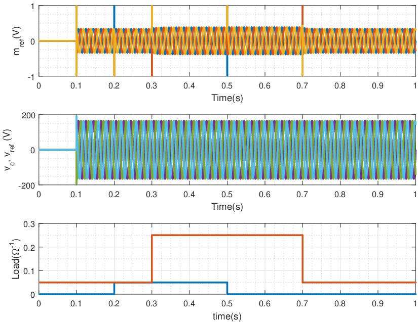
For the following simulation case study, we consider a converter rated in the 1010 KW range, with the choice of parameters as: id​c=100​A;Gd​c=0.1​Ω−1;Cd​c=0.001​F​;​R=0.1​Ω​;​L=5.10−4​H​;​C=10−5​Fi_{dc}=100A\mathchar 59\relax G_{dc}=0.1\Omega^{-1}\mathchar 59\relax C_{dc}=0.001F\mathord{\mathchar 59\relax}\,R=0.1\Omega\mathord{\mathchar 59\relax}\,L=5.10^{-4}H\mathord{\mathchar 59\relax}\,C=10^{-5}F yielding the reference signal defined by its amplitude v^=165​V\hat{v}=165V and frequency ωr​e​f=2​π​50​r​a​d/s\omega_{ref}=2\pi 50\,rad/s and nominal DC voltage of vd​c;r​e​f=1000​Vv_{dc\mathchar 59\relax ref}=1000V. This example of the reference vr​e​fv_{ref} could be interpreted as a three-phase Sinwave generator with an amplitude v^\hat{v} and ωr​e​f\omega_{ref} after transformation into (a​b​c)(abc)- frame.

In order to track the reference voltage vr​e​f{v}_{ref}, we choose the PI controller gains as

Kp​c=1;Ki​c=25000;Kp​l=250;λ0=−5⋅104s−1;λℓ=−5⋅105s−1.K_{pc}=1\,\mathchar 59\relax K_{ic}=25000\,\mathchar 59\relax K_{pl}=250\,\mathchar 59\relax\lambda_{0}=-5\cdot 10^{4}s^{-1}\,\mathchar 59\relax\lambda_{\ell}=-5\cdot 10^{5}s^{-1}\,.

Simulation results are depicted in Figure 2.
Refer to caption
Figure 2: Time-domain simulations of the modulation signal as control input of the DC/AC converter resulting from tracking a given reference signal across the capacitor vr​e​fv_{ref} while interfacing resistive and reactive load undergoing a step change.

The ongoing evolution of control strategies of DC/AC converters suggests that the reference signal vr​e​fv_{ref} can be itself generated from an upper controller called in the following as outer-loop control which takes into account other control purposes, related for instance to interfacing various inverters with a grid network. Next, we propose different forms of outer-loop controllers in order to generate a reference signal vr​e​fv_{ref} for the voltage across the capacitor, considered to be the converter terminal voltage, as shown in Figure 3, which can be tracked using the inner-loop controllers introduced above.

iα​βi_{\alpha\beta}- controllerDC/AC convertervα​βv_{\alpha\beta}-controllerouter-loop controllermα​βm_{\alpha\beta}Measurementsir​e​fi_{ref}vr​e​fv_{ref}exe_{x}eℓe_{\ell}−-iα​β;vd​ci_{\alpha\beta}\mathchar 59\relax v_{dc}−-vα​β;il​o​a​dv_{\alpha\beta}\mathchar 59\relax i_{load}
Figure 3: Control architecture for tracking a generated reference vr​e​fv_{ref} from an outer-loop controller forwarded to inner-loop control

2 Outer-loop: droop control

The vast majority of academic and industrial efforts approach real-time control challenges by means of droop control. Drawing from the control of synchronous generators in bulk power systems, droop control is a control approach which linearly trades off the active and reactive power injection with the inverter’s terminal-voltage amplitude and frequency [21]. This implies that there exists a relationship between the calculated power at the converter output and that of the voltage at its terminal.

We briefly review frequency droop control in resistive AC microgrids as described in [22]. The active power injection PP at each source is controlled to be proportional to its frequency deviation θ˙\dot{\theta} (from a nominal frequency θ˙0\dot{\theta}_{0}) as

θ˙=θ˙0+n⁡(P0−P);{\dot{\theta}=\dot{\theta}_{0}+n(P_{0}-P)}\,\mathchar 59\relax (5)

where θ˙0=ωr​e​f\dot{\theta}_{0}=\omega_{ref} is the nominal frequency, n>0n>0 refers to the frequency droop coefficient and P0∈[0;Pm​a​x]P_{0}\in[0\mathchar 59\relax P_{max}] is a nominal injection setpoint. Pm​a​xP_{max} is the maximal active power injection capacity of a source.

A key feature of AC frequency droop control in a network is that it synthesizes the synchronous frequency as a global variable indicating the load/generation imbalance in the microgrid [23].

We use the following amplitude droop controller, inducing a trade-off between the amplitude v^>0\hat{v}>0 to the reactive power at the terminals of the DC/AC converter denoted by QQ as follows

v^=v^0+d⁡(Q0−Q);{\hat{v}=\hat{v}_{0}+d\,(Q_{0}-Q)}\,\mathchar 59\relax (6)

where d>0d>0 represents the amplitude droop control coefficient, Q0∈[−Qm​a​x;Qm​a​x]Q_{0}\in[-Q_{max}\mathchar 59\relax Q_{max}] and v^0>0\hat{v}_{0}>0 refers to respectively the nominal setpoint of the reactive power and the amplitude at the converter output terminal voltage, corresponding to the voltage of the AC capacitor.

The reference voltage resulting from the implementation of the resistive droop control in (α​β)(\alpha\beta)- frame is given by

vr​e​f;d​r​o​o​p=v^​[−sin⁡(θ)cos⁡(θ)].v_{ref\mathchar 59\relax droop}=\hat{v}\begin{bmatrix}-\sin(\theta)\\ \cos(\theta)\end{bmatrix}\,. (7)

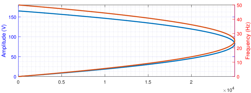
The curves in Figure 4 depict droop controller in amplitude as described in (6) and frequency as in (5).

Refer to caption
(a) Droop control in frequency for nominal setpoint (P0P_{0}, f0f_{0}) with f0=ωr​e​f/2​πf_{0}=\omega_{r}ef/2\pi
Refer to caption
(b) Droop control in amplitude for nominal setpoint (Q0Q_{0}, v0v_{0})
Figure 4: Curves of droop control method in amplitude v^>0\hat{v}>0 and frequency f=ϕ˙/2​πf=\dot{\phi}/2\pi

Summing up, the control scheme of this outer-loop controller can be described in (α​β)(\alpha\beta)- frame by the diagram 5.

iα​βi_{\alpha\beta}-controllerDC/AC convertervα​βv_{\alpha\beta}-controllerdroop-controllerReference Generatormα​βm_{\alpha\beta}Measurementsir​e​fi_{ref}P0​;​Q0P_{0}\mathord{\mathchar 59\relax}Q_{0}vr​e​f=v^​[−sin⁡(θ)cos⁡(θ)]⊤v_{ref}=\hat{v}\begin{bmatrix}-\sin(\theta)&\cos(\theta)\end{bmatrix}^{\top}−-iα​βi_{\alpha\beta}v0;ϕ0v_{0}\mathchar 59\relax\phi_{0}−-P​;​QP\mathord{\mathchar 59\relax}Q−-vα​βv_{\alpha\beta}
Figure 5: Control architecture for tracking a generated reference vr​e​fv_{ref} from an upper controller represented by droop control referenced by a generator setting nominal operating conditions.
Simulation results

We consider again the single inverter case as introduced previously. In order to design droop control in amplitude and frequency, we define the following nominal active and reactive power as well as the control gains

P0=104​W​;​Q0=2000​V​A​R​;​d=2⋅10−3​V/V​A​R​;​n=2⋅10−3​V/W.P_{0}=10^{4}W\mathord{\mathchar 59\relax}\,Q_{0}=2000VAR\mathord{\mathchar 59\relax}\,\,d=2\cdot 10^{-3}V/VAR\mathord{\mathchar 59\relax}\,\,n=2\cdot 10^{-3}V/W\,.

Simulation results in Figure 6 reflect droop control laws introduced in (6) and (5).

Refer to caption
Figure 6: Time-domain simulations of active and reactive power and its effect on the amplitude and frequency at the converter terminal voltage

Once the DC/AC converter operating in nominal conditions, is interfaced with active and reactive load, the reference in amplitude and frequency of the capacitor at the output of the DC/AC converter is reacting on an increase/decrease of the load by a decrease/increase in amplitude and frequency. This implies that the frequency and amplitude at the AC capacitor is adjusted to the load generation imbalance of single inverter case according to the resistive droop control law.

Remark 2.

Depending on the choice of the droop coefficients d;n>0d\mathchar 59\relax n>0 the droop in amplitude and frequency, one can define the trade-off to active and reactive power demand of the load. These gain coefficients have positive values in the droop control literature as in [21, 22].

Primary droop control achieves stable proportional load sharing in a fully decentralized way while respecting actuation constraints [22]. This strategy can be further extended via secondary control objectives comprising an optimal economic dispatch which defines a general optimization problem to be solved. This can be even more enhanced by means of tertiary control objectives aiming to correct the steady state and recover optimality via distributed averaging based control strategy [24], which requires the establishment of a communication, i.e local frequency sensing and neighborhood communication between the different decentralized controllers via modern techniques. Therefore, droop control lends itself useful to ensure stability of power networks and achieve economic dispatch between generators and controllable loads.

Despite its effectiveness in network regulation, droop control methods still presume the existence of a quasi-stationary sinusoidal steady state and operate mainly on phasor quantities [21]. In addition, it assumes the knowledge of given nominal active and reactive power references in advance, which are not always easy to obtain. Moreover, to the author’s knowledge inner control loops are always considered as "blackbox" and its dynamics are not explicitly included in the analysis of multiple inverters connected to a grid network, which makes relevant signals almost non-tractable.

3 Outer-loop: virtual oscillator controller

We study a recently approached control scheme that ensures network stability of power electronic inverters by emulating the dynamics of the Van der Pol oscillator. This compelling time-domain alternative presents a novel control strategy to generate nonlinear oscillations, known for their robustness and structural stability as well as the existence of an only one and unique isolated periodic orbit in comparison to a continuum of closed orbits for harmonic oscillators [1].

Virtual oscillator control (VOC) refers to a digital control strategy emulating the behavior of oscillators like that of Van der Pol, programmed on real micro-controllers and applied to H-bridge inverters.

1 Oscillator-based reference generation

Van der Pol oscillator in closed-loop fashion

The Van der Pol oscillator can be described by the following dynamics [1]

x˙1\displaystyle\dot{x}_{1} =x2\displaystyle=x_{2} (8a)
x˙2\displaystyle\dot{x}_{2} =−x1+μ⁡(1−x12)​x2;\displaystyle=-x_{1}+\mu(1-x_{1}^{2})x_{2}\,\mathchar 59\relax (8b)

with μ>0\mu>0 is a parameter to be specified.
This ordinary differential equation, which was used by Van der Pol to study oscillations in vacuum tube circuits, is a fundamental example in nonlinear oscillations theory. It is an equation describing self-sustaining oscillations, in which the net exchange of energy over one cycle is zero. It possesses a periodic solution that attracts every other solution except the zero [1]. Depending on the values of μ\mu, a small (0.2)(0.2), medium (1.0)(1.0) or large value (5.0)(5.0), we can get different forms of phase portrait of Van der Pol as depicted in Figure 7. If μ=0\mu=0, the equation reduces to that of a simple harmonic motion

x˙1\displaystyle\dot{x}_{1} =−x2\displaystyle=-x_{2}
x˙2\displaystyle\dot{x}_{2} =x1.\displaystyle=x_{1}\,.

The parameter μ>0\mu>0 determines as well how fast/slow the dynamics of Van der Pol oscillator are [1].

Refer to caption
Figure 7: Limit cycle oscillations for different values of the parameter μ>0\mu>0 with y=x1y=x_{1} and y′=x2y^{\prime}=x_{2} [26]

The emulation of Van der Pol goes usually by implementing an oscillator model as in [10] composed of a linear subsystem consisting of an RLC circuit, set in parallel with a nonlinear voltage-dependent current source. The special choice of this current source is based on emulating the nonlinearity of Van der Pol for a given μ>0\mu>0.

In comparison to the commonly used single-phase model, we design a nonlinear virtual oscillator for the three-phase DC/AC converter by implementing a virtual oscillator emulating Van der Pol for each phase in (α​β)(\alpha\beta)- frame. We design a feedback oscillator controller for the α\alpha- component as described in [21].

x˙1​;​α\displaystyle\dot{x}_{1\mathord{\mathchar 59\relax}\alpha} =ω0​x2​;​α\displaystyle=\omega_{0}x_{2\mathord{\mathchar 59\relax}\alpha}
x˙2​;​α\displaystyle\dot{x}_{2\mathord{\mathchar 59\relax}\alpha} =−ω0​x1​;​α+μ⁡(1−x1​;​α2)​x2​;​α+κ​il​o​a​d;α​(t);\displaystyle=-\omega_{0}x_{1\mathord{\mathchar 59\relax}\alpha}+\mu(1-x_{1\mathord{\mathchar 59\relax}\alpha}^{2})x_{2\mathord{\mathchar 59\relax}\alpha}+\kappa i_{load\mathchar 59\relax\alpha}(t)\,\mathchar 59\relax

and a second oscillator for the β\beta- component defined by

x˙1​;​β\displaystyle\dot{x}_{1\mathord{\mathchar 59\relax}\beta} =ω0​x2​;​β\displaystyle=\omega_{0}x_{2\mathord{\mathchar 59\relax}\beta}
x˙2​;​β\displaystyle\dot{x}_{2\mathord{\mathchar 59\relax}\beta} =−ω0​x1​;​β+μ⁡(1−x1​;​β2)​x2​;​β+κ​il​o​a​d​;​β​(t);\displaystyle=-\omega_{0}x_{1\mathord{\mathchar 59\relax}\beta}+\mu(1-x_{1\mathord{\mathchar 59\relax}\beta}^{2})x_{2\mathord{\mathchar 59\relax}\beta}+\kappa i_{load\mathord{\mathchar 59\relax}\beta}(t)\,\mathchar 59\relax

with κ>0\kappa>0 and the load current defined as

il​o​a​d=[iα​;​l​o​a​diβ​;​l​o​a​d].i_{load}=\begin{bmatrix}i_{\alpha\mathord{\mathchar 59\relax}load}\\ i_{\beta\mathord{\mathchar 59\relax}load}\end{bmatrix}\,.
Remark 3 (VOC and droop control [11]).

The virtual oscillator control stabilizes arbitrary initial conditions to a sinusoidal steady state, while droop control acts on the phasor quantities and is only well-defined in the sinusoidal steady state as depicted in the Figure 8, where the voltage vv is accounting for the α\alpha- component and the current ii for the β\beta- component for a circuit realization of Van der Pol oscillator. Hence, droop control and VOC can be implemented together to stabilize AC signals to waveforms with a predefined time-scale separation between the two controllers [11].

Refer to caption
Figure 8: Representation of Droop control laws as embedded within the nonlinear dynamics of Van der Pol Oscillators.
Choice of initial conditions

The Van der Pol oscillator is defined in (8) in Cartesian coordinates. For each phase, we redefine the oscillator dynamics in polar coordinates as follows for the α\alpha- component

v^α\displaystyle\hat{v}_{\alpha} =x1​;​α2+x2​;​α2\displaystyle=\sqrt{x_{1\mathord{\mathchar 59\relax}\alpha}^{2}+x_{2\mathord{\mathchar 59\relax}\alpha}^{2}}
ϕα\displaystyle\phi_{\alpha} =arctan⁡(x1​;​αx2​;​α);\displaystyle=\arctan\left(\frac{x_{1\mathord{\mathchar 59\relax}\alpha}}{x_{2\mathord{\mathchar 59\relax}\alpha}}\right)\,\mathchar 59\relax

and the β\beta- component as follows

v^β\displaystyle\hat{v}_{\beta} =x1​;​β2+x2​;​β2\displaystyle=\sqrt{x_{1\mathord{\mathchar 59\relax}\beta}^{2}+x_{2\mathord{\mathchar 59\relax}\beta}^{2}}
ϕβ\displaystyle\phi_{\beta} =arctan⁡(x1​;​βx2​;​β).\displaystyle=\arctan\left(\frac{x_{1\mathord{\mathchar 59\relax}\beta}}{x_{2\mathord{\mathchar 59\relax}\beta}}\right)\,.

Leveraging the fact that the angles of the virtual inductor current and capacitor voltage are orthogonal as introduced in [10] (corresponding here to angles of x1​;​αx_{1\mathord{\mathchar 59\relax}\alpha} and x1​;​βx_{1\mathord{\mathchar 59\relax}\beta} signals), we initialize the α\alpha- and β\beta- oscillators orthogonally such that the following holds

ϕα​(0)−ϕβ​(0)\displaystyle\phi_{\alpha}(0)-\phi_{\beta}(0) =π2+k​π​;​k∈Z\displaystyle=\frac{\pi}{2}+k\pi\mathord{\mathchar 59\relax}\,k\in Z
v^α​(0)\displaystyle\hat{v}_{\alpha}(0) =v^β​(0).\displaystyle=\hat{v}_{\beta}(0)\,.

That is both oscillators in α\alpha- and β\beta- components are initialized with the same initial amplitude. We then apply a transformation from (α​β)(\alpha\beta) to (a​b​c)(abc)- frame to yield three-phase signals.

We assume that, once we start with orthogonal α\alpha and β\beta components, this condition is not violated for all times t>0t>0, which turns out to be well-justified by our simulations.

In summary, we define the reference given by the outer-loop virtual oscillator controller for the AC capacitor voltage as

vr​e​f​;​v​o​c=v^v​o​c​[x1​;​αx1​;​β]=v^​32​[sin⁡(θ)cos⁡(θ)]​;​θ˙​(t)=ωr​e​f​;​t>0.v_{ref\mathord{\mathchar 59\relax}voc}=\hat{v}_{voc}\begin{bmatrix}x_{1\mathord{\mathchar 59\relax}\alpha}\\ x_{1\mathord{\mathchar 59\relax}\beta}\end{bmatrix}=\hat{v}\sqrt{\frac{3}{2}}\begin{bmatrix}\sin(\theta)\\ \cos(\theta)\end{bmatrix}\mathord{\mathchar 59\relax}\,\dot{\theta}(t)=\omega_{ref}\mathord{\mathchar 59\relax}\,t>0\,.

We design the amplitude v^v​o​c\hat{v}_{voc} such that

v^v​o​c=v^r​e​f​32x1​;​α2+x1​;​β2.\hat{v}_{voc}=\frac{\hat{v}_{ref}\sqrt{\frac{3}{2}}}{\sqrt{x_{1\mathord{\mathchar 59\relax}\alpha}^{2}+x_{1\mathord{\mathchar 59\relax}\beta}^{2}}}\,.
Simulation results

We simulate the DC/AC converter using the following VOC parameters

μ=0.2​s−1​;​κ=0.8​V/s​A;\mu=0.2s^{-1}\mathord{\mathchar 59\relax}\,\kappa=0.8V/sA\,\mathchar 59\relax

in order to obtain the reference signal for the voltage across the AC capacitor

ωr​e​f=2​π​50​r​a​d/s​;​v^=165​V;\omega_{ref}=2\pi 50\,rad/s\mathord{\mathchar 59\relax}\,\hat{v}=165V\,\mathchar 59\relax

with the initial conditions of the states x1​;​x2x_{1}\mathord{\mathchar 59\relax}\,x_{2}

x1​;​α​(0)=−x2​;​α​(0)=x1​;​β​(0)=x2​;​β​(0)=1​V;x_{1\mathord{\mathchar 59\relax}\alpha}(0)=-x_{2\mathord{\mathchar 59\relax}\alpha}(0)=x_{1\mathord{\mathchar 59\relax}\beta}(0)=x_{2\mathord{\mathchar 59\relax}\beta}(0)=1V\,\mathchar 59\relax

such that the following condition is satisfied

ϕα​(0)−ϕβ​(0)=π2;v^α​(0)=v^β​(0)=1.4142​V;\phi_{\alpha}(0)-\phi_{\beta}(0)=\frac{\pi}{2}\,\mathchar 59\relax\hat{v}_{\alpha}(0)=\hat{v}_{\beta}(0)=1.4142V\,\mathchar 59\relax

and initialized with a fully charged DC capacitor units vd​c​(0)=1000​Vv_{dc}(0)=1000V.

Simulation results are shown in Figure 9, when load/ no load is acting on the converter

(a) A zoomed version around t=0​st=0s of time domain simulations of the virtual oscillator control using Van der Pol oscillator
(b) Time domain simulations of the virtual oscillator control using van der Pol oscillator
(c) Time-domain simulations with resistve and reactive load
(d) Time-domain simulations with resistve and reactive load
Figure 9: Time-domain simulations of upper controller represented by Van der Pol oscillations for reference generation
Outer loop: Polar VOC in closed-loop fashion

We consider an alternative of implementing virtual oscillator controllers (VOC), which is the polar virtual oscillator considered to be an outer loop control generating a reference vr​e​f;p​o​l​a​rv_{ref\mathchar 59\relax polar} that is handed over to the inner-loop control as depicted in Figure 3. In other words, the voltage across the capacitor is referenced by a polar virtual oscillator controller. In fact, we use the features of droop methods mainly the trade-off between active and reactive power to frequency and amplitude of vr​e​f​;​p​o​l​a​rv_{ref\mathord{\mathchar 59\relax}polar}, for the implementation of the polar VOC dynamics in order to assure network regulation among many other properties inherited from the droop control method. We can write the control law as follows

vr​e​f​;​p​o​l​a​r\displaystyle v_{ref\mathord{\mathchar 59\relax}polar} =v^​32​[−sin⁡(θ)cos⁡(θ)]\displaystyle=\hat{v}\,\sqrt{\frac{3}{2}}\begin{bmatrix}-\sin(\theta)\\ \cos(\theta)\end{bmatrix}
θ˙\displaystyle\dot{\theta} =θ˙0+d⁡(P0−P)\displaystyle=\dot{\theta}_{0}+d\,(P_{0}-P)
v^˙\displaystyle\dot{\hat{v}} =λo​s​c​(v^0+n⁡(Q0−Q)−v^)​;​λo​s​c>0.\displaystyle=\lambda_{osc}(\hat{v}_{0}+n\,(Q_{0}-Q)-\hat{v})\mathord{\mathchar 59\relax}\,\lambda_{osc}>0\,.
Simulation results

We simulate the DC/AC converter using the following parameters

Q0\displaystyle Q_{0} =2000​V​A​R​;​P0=10000​W​;​d=0.002​V/W​;​n=0.001​V/V​A​R;\displaystyle=2000VAR\mathord{\mathchar 59\relax}\,P_{0}=10000W\mathord{\mathchar 59\relax}\,d=0.002V/W\mathord{\mathchar 59\relax}\,n=0.001V/VAR\mathchar 59\relax
ϕ˙0\displaystyle\dot{\phi}_{0} =2​π​50​r​a​d​;​v^0=165​V​;​λo​s​c=100​s−1;\displaystyle=2\pi 50\,rad\mathord{\mathchar 59\relax}\,\hat{v}_{0}=165V\mathord{\mathchar 59\relax}\,\lambda_{osc}=100s^{-1}\,\mathchar 59\relax

and the initial condition for the DC voltage vd​c​(0)=0v_{dc}(0)=0. Simulation results are depicted in Figure 10.

Figure 10: Time-domain simulations of polar VOC in closed-loop fashion, implementing resistive droop control as reference in amplitude and angle after a step change in the load conductance and suseptance

2 Oscillator-based modulation assignment

We aim to directly assign a sinusoid to the converter input, namely the modulation signal mα​βm_{\alpha\beta} without using inner-loop control architecture, thus an open-loop control. We introduce in the following the open-loop controller based on virtual oscillations in polar coordinates and defined in (α​β)(\alpha\beta)- frame. Indeed, we define the polar oscillator for the modulation signal by its amplitude and angle defined by

mo​p​e​n−l​o​o​p\displaystyle m_{open-loop} =v^m​32​[−sin⁡(θm)cos⁡(θm)]\displaystyle=\hat{v}_{m}\sqrt{\frac{3}{2}}\begin{bmatrix}-\sin(\theta_{m})\\ \cos(\theta_{m})\end{bmatrix}
v^˙m\displaystyle\dot{\hat{v}}_{m} =λm​(v^m​;​r​e​f−v^)\displaystyle=\lambda_{m}\,(\hat{v}_{m\mathord{\mathchar 59\relax}ref}-\hat{v})
θ˙m\displaystyle\dot{\theta}_{m} =ωr​e​f;\displaystyle=\omega_{ref}\,\mathchar 59\relax

with λm>0\lambda_{m}>0.

Simulation results

We now simulate the open-loop polar oscillator controller using the following parameters.

λm\displaystyle\lambda_{m} =100​s−1​;​v^=165​V​;​ωr​e​f=2​π​50​r​a​d/s​;​v^m;r​e​f=2​v^vd​c​;​r​e​f=0.33​V​;\displaystyle=100s^{-1}\mathord{\mathchar 59\relax}\,\hat{v}=165V\mathord{\mathchar 59\relax}\,\omega_{ref}=2\pi 50\,rad/s\mathord{\mathchar 59\relax}\,\hat{v}_{m\mathchar 59\relax ref}=\frac{2\hat{v}}{v_{dc\mathord{\mathchar 59\relax}ref}}=0.33V\mathord{\mathchar 59\relax}
vd​c​;​r​e​f\displaystyle v_{dc\mathord{\mathchar 59\relax}ref} =id​cGd​c​;;\displaystyle=\frac{i_{dc}}{G_{dc}}\mathord{\mathchar 59\relax}\,\,\mathchar 59\relax

where v^m;r​e​f\hat{v}_{m\mathchar 59\relax ref} is chosen accordingly in order to get a capacitor voltage of amplitude v^=165​V\hat{v}=165V and frequency ωr​e​f\omega_{ref}. Simulation results are depicted in Figure 11.

(a) Time domain simulation of modulation signal and capacitor voltage of polar VOC
Refer to caption
(b) Evolution of amplitude and frequency of the modulation signal
Figure 11: Simulation results of the virtual oscillator in polar coordinates

The polar virtual oscillator in open-loop is comparable to a sinwave generator with amplitude v^m\hat{v}_{m} and a frequency ωr​e​f\omega_{ref}. It has been extended to closed-loop fashion for oscillator-based reference generation by selecting a relevant feedback state corresponsing to the amplitude and frequency of the AC capacitor to accommodate our control objectives. Next, we review a further outer-loop control design using virtual synchronous machine (VSM) algorithms.

4 Outer-loop: virtual synchronous machines

Recent research centralizes in favor of new aggregation and control techniques, where synchronous machines (SM) are gradually replaced by power-electronics based devices, capable of emulating the rotational inertia of SM. These intelligent devices named in the following as virtual synchronous machines (VSM) promise an autonomous operation aiming to ultimately increase the inertia constant for a given power system [3].

If the goal of the VSM is to emulate the inertia and damping properties of the SM, then these two main aspects can be readily captured by the swing equation known as

J​ω˙=Tm−Te−D​ω;J\dot{\omega}=T_{m}-T_{e}-D\omega\,\mathchar 59\relax

where J>0J>0 is the rotor inertia, ω∈\omega\in\real the rotating speed of the machine relative to an absolute frequency ωr​e​f\omega_{ref}, Tm∈T_{m}\in\real the mechanical, whereas TeT_{e} is the electromagnetic torque, D>0D>0 is a damping coefficient accounting for the damping torque associated with the damping windings during transient conditions. It can be expressed in terms of power instead by multiplying all terms by the relative frequency ω\omega. For small oscillations around the synchronous conditions, the power balance can be expressed by the following

M​ω˙=Pm−Pe−D′​ω;M\dot{\omega}=P_{m}-P_{e}-D^{\prime}\omega\,\mathchar 59\relax (19)

with M=ω​J​;​D′=ω​DM=\omega J\mathord{\mathchar 59\relax}\,D^{\prime}=\omega D.

The widely-used approach to implement VSM is by providing a reference frequency ω\omega to inner-loop control. VSM is proved to be equivalent to conventional droop-based methods for standalone and micro-grid operation of converters according to the following scheme in Figure 12, where the block Virtual Inertia and Power Control implements the swing equation described previously in (19).

Refer to caption
Figure 12: VSM with cascaded voltage and current loops [4]

Most important topologies rely on interfacing mathematical SM models with power electronic converters arranged with a cascade of controllers which receive reference signals from the VSM and translate them into gate signals for the inverter [4], designed by inner-loop control. The implementation of the VSM implies an embedded controller computer calculating the references [5] or a digital signal processor (DSP) associated to a circuit running under special program to control the switches as in the so-called Synchroverters [6]. An abundant usage of Phase Locked Loops (PLL) ranges from locking the electric power system waveform [3] to generating a reference for the VSM [7] reveals a high dependency on real-time frequency measurements as depicted in an example of realization in Figure 12.

Indeed, frequency estimation and accurate tracking is critical for VSM algorithm and affects its performance [4]. Moreover, filter delays and measurement channels often degrade the simulation results [4].

On the other hand, a proper dynamic modeling is a key issue to tackle the inaccuracy in power system simulation by including a full description of its dynamics in transients and at steady state for different operating points. For instance, the swing equation corresponding to the reference model and serving as basis for VSM algorithms, gives only good approximation of frequency transient during the first couple of seconds directly after the power imbalance. Moreover, inner PI loops are non-tractable "blackbox", due to the cascaded control architecture which is difficult to analyze and to keep track of the relevant control signals. On longer terms, other control actions are needed besides the inertia to determine the frequency response [27]. New perspective of implementing virtual inertia has been proposed in [9], where a super-capacitor connected to the DC-link, responsible for mimicking the mass behavior, outperforms the virtual rotating mass by improving the system stability independently of the disturbance moment [9]. Nevertheless, it remains a conservative way of using the voltage at DC-link.

As a summary, by reviewing the traditional approach of controlling DC/AC converter, we presented the inner-loop as innermost control hierarchy responsible for tracking a given reference generated from higher-level control loop. Different studies investigate a proper choice of these outer-loops ranging from droop to oscillator-based and virtual synchronous machine methods. Nonetheless different challenges arise, while implementing these controllers due to merely hard-to-justify assumptions, for instance a quasi-stationary steady state (not valid e.g in the case of a blackout), operation on phasor or large-time delay which may deteriorate system performance. In these settings, inner loops (PI) are mostly non-tractable and considered as "blackbox" due to the complexity of the analysis of such hierarchical dynamics.

Chapter 3 Matching control of the synchronous machines

Taking into account all the difficulties imposed by conventional DC/AC control studies targeting to compensate for the retirement of SMs and their ancillary services, we aim to design a controller able to emulate a SM model by making use of the physical storage available in a DC/AC converter.

We introduce an innovative approach that makes use of the natural storage element in the DC circuit of power electronics converter and structurally equivalences a DC/AC converter with a SM by matching the two models. A major difference to the VSM, is that no external referencing is needed at the converter terminal voltage. Moreover, our control strategy does not require additional inner control loops for tracking signals. Instead, it widens the scope of the utility of DC circuit with its natural storage in the regulation mechanism of power systems by including it explicitly and in a more effective way. A proper system modeling involving DC and AC side dynamics is presented for this purpose. The structural equivalence, due to different physical sizes between a converter and SM, does not influence the performance of the proposed controller and offers more flexibility in tuning it. Since DC measurements are easier to obtain and do not impose additional time delays in comparison to the usual AC measurements required by VSM algorithms, the inverter in closed-loop fashion is advantageous and even more reliable. Another appealing property of the approached controller is that it is well-defined under all operating condition, since it interfaces with recent research field, that of virtual oscillators control (VOC) as in [10, 11] and this by means of the controller dynamics which encode the inverter terminal dynamics, i.e the dynamics at the output voltage of the converter as a nonlinear limit cycle oscillator adapting to the grid state.

1 The synchronous machine model

The aim of this section is to highlight a particular structure of the SM model which lends itself useful in designing a matching feedback controller for the 33-phase DC/AC converter. We consider a single-pole-pair, non-salient rotor, externally excited SM in (α​β)(\alpha\beta)-frame as in [2], together with an output AC capacitor at the terminals of the converter, described by the following state space model:

θ˙\displaystyle\dot{\theta} =ω\displaystyle=\omega (1a)
M​ω˙\displaystyle M\dot{\omega} =−D​ω+τm−τe\displaystyle=-D\omega+\tau_{m}-\tau_{e} (1b)
C​v˙α​β\displaystyle C\,\dot{v}_{\alpha\beta} =−il​o​a​d+iα​β\displaystyle=-i_{load}+i_{\alpha\beta} (1c)
λ˙α​β\displaystyle\dot{\lambda}_{\alpha\beta} =−R​iα​β−vα​β.\displaystyle=-Ri_{\alpha\beta}-v_{\alpha\beta}\,. (1d)

Here M>0M>0 and D>0D>0 are the rotor inertia and damping, τm\tau_{m} is the driving mechanical torque, and τe\tau_{e} is the electrical torque. We denote the rotor angle by θ∈𝕊1\theta\in\mathbb{S}^{1}, its angular velocity by ω\omega, the magnetic flux in the stator winding by λα​β\lambda_{\alpha\beta}, and the stator resistance by R>0R>0. At its terminals the machine is interfaced to the grid through a shunt capacitor with capacitance C>0C>0 and capacitor voltage vα​βv_{\alpha\beta}, and the terminal load current (exciting the machine) is denoted by il​o​a​di_{load}.

Assumption 1.1 (Regulated rotor field current).

The rotor winding described by the magnetic flux λf\lambda_{f}, is omitted in our equations in (1) but it is considered with the assumption that the rotor current ifi_{f}, defined in the following, is externally regulated to a constant value [2].

We define the electromagnetic energy in the machine WeW_{e} as

We=[λα​β⊤λf]​Lθ−1​[λα​βλf];W_{e}=\begin{bmatrix}\lambda_{\alpha\beta}^{\top}&\lambda_{f}\end{bmatrix}L_{\theta}^{-1}\begin{bmatrix}\lambda_{\alpha\beta}\\ \lambda_{f}\end{bmatrix}\,\mathchar 59\relax

where we made use of the inductance matrix LθL_{\theta}

Lθ=[Ls0Lm​cos⁡(θ)0LsLm​sin⁡(θ)Lm​cos⁡(θ)Lm​sin⁡(θ)Lf];L_{\theta}=\begin{bmatrix}L_{s}&0&L_{m}\cos(\theta)\\ 0&L_{s}&L_{m}\sin(\theta)\\ L_{m}\cos(\theta)&L_{m}\sin(\theta)&L_{f}\end{bmatrix}\,\mathchar 59\relax

where Lm>0L_{m}>0 is the stator-to-rotor mutual inductance, Ls>0L_{s}>0 the stator inductance and Lf>0L_{f}>0 the winding field inductance. We obtain the following expressions the inductance current iα​β∈2i_{\alpha\beta}\in\real^{2}

[iα​βif]=[∂We∂λα​β∂We∂λf]=Lθ−1​[λα​βλf];\begin{bmatrix}i_{\alpha\beta}\\ i_{f}\end{bmatrix}=\begin{bmatrix}\frac{\partial W_{e}}{\partial\lambda_{\alpha\beta}}\\ \frac{\partial W_{e}}{\partial\lambda_{f}}\end{bmatrix}=L_{\theta}^{-1}\begin{bmatrix}\lambda_{\alpha\beta}\\ \lambda_{f}\end{bmatrix}\,\mathchar 59\relax (2)

and for the electrical torque τe\tau_{e}

τe=∂We∂θ=−iα​β⊤​Lm​if​[−sin⁡(θ)cos⁡(θ)].\tau_{e}=\frac{\partial W_{e}}{\partial\theta}=-i_{\alpha\beta}^{\top}L_{m}i_{f}\begin{bmatrix}-\sin(\theta)\\ \cos(\theta)\end{bmatrix}\,. (3)

By using identity (2) in equation (1d), we express the stator dynamics in terms of current as

Ls​(iα​β)˙=−R​iα​β−vα​β−θ˙​Lm​if​[−sin⁡(θ)cos⁡(θ)].L_{s}\dot{(i_{\alpha\beta})}=-Ri_{\alpha\beta}-v_{\alpha\beta}-\dot{\theta}L_{m}i_{f}\begin{bmatrix}-\sin(\theta)\\ \cos(\theta)\end{bmatrix}\,. (4)

Note that we can identify the electromotive force (EMF) in the machine as the last term in (4). As a summary, we rewrite (1) as follows

θ˙\displaystyle\dot{\theta} =ω\displaystyle=\omega (5a)
M​ω˙\displaystyle M\dot{\omega} =−D​ω+τm+iα​β⊤​Lm​if​[−sin⁡(θ)cos⁡(θ)]\displaystyle=-D\omega+\tau_{m}+i_{\alpha\beta}^{\top}L_{m}i_{f}\begin{bmatrix}-\sin(\theta)\\ \cos(\theta)\end{bmatrix} (5b)
C​v˙α​β\displaystyle C\dot{v}_{\alpha\beta} =−il​o​a​d+iα​β\displaystyle=-i_{load}+i_{\alpha\beta} (5c)
Ls​(i˙α​β)\displaystyle L_{s}(\dot{i}_{\alpha\beta}) =−R​iα​β−vα​β−ω​Lm​if​[−sin⁡(θ)cos⁡(θ)].\displaystyle=-Ri_{\alpha\beta}-v_{\alpha\beta}-\omega L_{m}i_{f}\begin{bmatrix}-\sin(\theta)\\ \cos(\theta)\end{bmatrix}\,. (5d)

Observe the similarities between the converter model (15) and the SM model (5), where the dynamics of DC circuit can be seen as analogous to the rotor mass dynamics. Notice that, structurally, the electrical torque and electromotive force here play a role similar to ixi_{x} and vxv_{x} in the converter model (15).

2 The synchronous machine matching control

In this section, we propose a control scheme for the modulation signal mα​β∈2m_{\alpha\beta}\in\real^{2} in (15), which matches the closed-loop dynamics of the converter to the dynamics of the SM in (5).

The first step is to introduce the virtual angle θv\theta_{v} to resemble to the rotor angle of the SM and assign to it the following dynamics

θ˙v=η​vd​c;\boxed{\dot{\theta}_{v}=\eta\,v_{dc}}\;\mathchar 59\relax (6)

where η>0\eta>0 is a constant gain to be specified. For example, a reasonable choice would be the ratio between the nominal AC frequency and the DC voltage reference since this choice induces the correct oscillation in the electrical domain.

The second step in control design is to assign a sinusoidal modulation scheme according to the following map mα​β:𝕊1→𝕊μ1{x∈2:‖x‖2=μ}m_{\alpha\beta}:\mathbb{S}^{1}\to\mathbb{S}^{1}_{\mu}\left\{x\in\real^{2}:\left\lVert x\right\rVert_{2}=\mu\right\}, such that

mα​β=μ​[−sin⁡(θv)cos⁡(θv)];\boxed{m_{\alpha\beta}=\mu\begin{bmatrix}-\sin(\theta_{v})\\ \cos(\theta_{v})\end{bmatrix}}\;\mathchar 59\relax (7)

where θv∈𝕊1\theta_{v}\in\mathbb{S}^{1} is an angle to be specified with the frequency θ˙\dot{\theta} as determined in (6), while the gain μ∈]0;1]\mu\in]0\mathord{\mathchar 59\relax}1] is constant and represents an amplitude for the modulation sinusoid.

By using (7), we can now write ixi_{x} and vxv_{x} as:

ix=12​iα​β⊤​μ​[−sin⁡(θv)cos⁡(θv)]​;​vx=12​vd​c​μ​[−sin⁡(θv)cos⁡(θv)].i_{x}=\frac{1}{2}i_{\alpha\beta}^{\top}\,\mu\begin{bmatrix}-\sin(\theta_{v})\\ \cos(\theta_{v})\end{bmatrix}\mathord{\mathchar 59\relax}\,v_{x}=\frac{1}{2}v_{dc}\,\mu\begin{bmatrix}-\sin(\theta_{v})\\ \cos(\theta_{v})\end{bmatrix}\,. (8)

We now complete the comparison between the generator model (5) and the closed-loop converter model (15) under the control scheme (7), (6). For this purpose, we identify the average switch voltage vxv_{x} with a virtual electromotive force by defining the following relation

μ=−2​η​Lm​if.\mu=-2\eta L_{m}i_{f}\,. (9)

By means of (3), (8) and (9), we identify the DC-side average switching current ixi_{x} with a virtual electrical torque by defining:

τe​;​v=1η⋅12​iα​β⊤​μ​[−sin⁡(θv)cos⁡(θv)]=1η​ix.\tau_{e\mathord{\mathchar 59\relax}v}=\frac{1}{\eta}\cdot\frac{1}{2}i_{\alpha\beta}^{\top}\,\mu\,\begin{bmatrix}-\sin(\theta_{v})\\ \cos(\theta_{v})\end{bmatrix}=\frac{1}{\eta}i_{x}\,. (10)

Next, we denote the virtual angular velocity by ωv=η​vd​c\omega_{v}=\eta\,v_{dc} and rewrite the equivalent closed-loop model for the DC/AC converter after dividing by η2\eta^{2} to relate τe​;​v\tau_{e\mathord{\mathchar 59\relax}v}, as in (10)

θ˙v\displaystyle\dot{\theta}_{v} =ωv\displaystyle=\omega_{v} (11a)
Cd​cη2​ω˙v\displaystyle\frac{C_{dc}}{\eta^{2}}\dot{\omega}_{v} =−Gd​cη2​ωv+id​c/η−1η​ix\displaystyle=-\frac{G_{dc}}{\eta^{2}}\omega_{v}+i_{dc}/{\eta}-\frac{1}{\eta}i_{x} (11b)
L​(iα​β)˙\displaystyle L\dot{(i_{\alpha\beta})} =−R​iα​β−vα​β+12​η​ωv​mα​β\displaystyle=-Ri_{\alpha\beta}-v_{\alpha\beta}+\frac{1}{2\eta}\omega_{v}m_{\alpha\beta} (11c)
C​v˙α​β\displaystyle C\dot{v}_{\alpha\beta} =−Gg​vα​β+iα​β.\displaystyle=-G_{g}v_{\alpha\beta}+i_{\alpha\beta}\,. (11d)

By attributing proper units to η\eta, we can now identify Cd​c/η2​;​Gd​c/η2C_{dc}/\eta^{2}\mathord{\mathchar 59\relax}\,G_{dc}/\eta^{2}, and id​c/ηi_{dc}/\eta respectively with the mechanical inertia typically 33 orders of magnitude (in p.u.) less than the inertia of a SM, a significant gain in equivalent damping factor, and driving torque of an equivalent SM.

Matching vs. virtual emulation

Observe that the structural equivalence of the closed-loop dynamics (11) to those of a SM is of purely physical nature as opposed to virtual, such as in the works of [13, 4, 3]. In recent works, the behavior of the SM is emulated in software, i.e with virtual storage elements which further provide set points for the inner-loop of the converter control, for which a time-scale separation is assumed. In comparison, we use the physical storage already present in the DC capacitor, which is reflected in the size of the equivalent inertia Cd​cη2\frac{C_{dc}}{\eta^{2}} and equivalent damping factor Gd​cη2\frac{G_{dc}}{\eta^{2}}, typically 3. order of magnitude less than the inertia of a SM.

Virtual adaptive oscillator interpretation

By defining ξ∈2\xi\in\real^{2} as a controller state and mα​βm_{\alpha\beta} as an output, we can rewrite the controller (7) and (6) as the nonlinear dynamic feedback oscillator

ξ˙=η​vd​c​[0−110]​ξ;mα​β=μ​ξ;\dot{\xi}=\eta\,v_{dc}\begin{bmatrix}0&-1\\ 1&0\end{bmatrix}\xi\,\mathchar 59\relax m_{\alpha\beta}=\mu\,\xi\,\mathchar 59\relax (12)

where ‖ξ⁡(0)‖2=1\left\lVert\xi(0)\right\rVert_{2}=1. As depicted in Figure 1, we can interpret the emulation control (7),(6) as an oscillator with constant amplitude ‖m⁡(0)‖2=μ\left\lVert m(0)\right\rVert_{2}=\mu and state-dependent frequency ωv=η​vd​c\omega_{v}=\eta\,v_{dc} in feedback with the DC/AC converter dynamics (15). This control strategy structurally resembles the classic proportional resonant control [14] with the difference that the frequency of the oscillator (12) actually adapts to the DC voltage which again reflects the grid state.

□\square

Cd​c​v˙d​c=−Gd​c​vd​c+id​c−12​mα​β⊤​iα​βL​i˙α​β=−R​iα​β+12​mα​β​vd​c−vα​βC​v˙α​β=−il​o​a​d+iα​β\begin{matrix}C_{dc}\dot{v}_{dc}=-G_{dc}v_{dc}+i_{dc}-\frac{1}{2}m_{\alpha\beta}^{\top}i_{\alpha\beta}\\ L\dot{i}_{\alpha\beta}=-Ri_{\alpha\beta}+\frac{1}{2}m_{\alpha\beta}v_{dc}-v_{\alpha\beta}\\ C\dot{v}_{\alpha\beta}=-i_{load}+i_{\alpha\beta}\end{matrix}ξ˙=η​vd​c​[01−10]​ξ\begin{matrix}\dot{\xi}=\eta\,v_{dc}\begin{bmatrix}0&1\\ -1&0\end{bmatrix}\xi\\ \end{matrix} μ\muη\eta(id​c,−il​o​a​d)(i_{dc}\mathchar 59\relax-i_{load}\,)(vd​c;vα​β)\,(v_{dc}\mathchar 59\relax v_{\alpha\beta})mα​βm_{\alpha\beta}vd​cv_{dc}−-
Figure 1: Closed-loop system comprising the converter dynamics (15) and the controller dynamics (12).
Remark 4 (Dynamics of γ\gamma- component ).

We now consider the γ\gamma-component of the converter AC signals. By construction of the modulation vector, we have vx​;​γ=0v_{x\mathord{\mathchar 59\relax}\gamma}=0. If we assume a balanced load, then il​o​a​d​;​γ=0i_{load\mathord{\mathchar 59\relax}\gamma}=0. We are left with the following asymptotically stable dynamics for the γ\gamma-component:

L​(iγ)˙\displaystyle L\dot{(i_{\gamma})} =−R​iγ−vγ\displaystyle=-Ri_{\gamma}-v_{\gamma} (13a)
C​v˙γ\displaystyle C\dot{v}_{\gamma} =iγ.\displaystyle=i_{\gamma}\,. (13b)

Since (13) is an asymptotically stable dynamical system, the omission of the γ\gamma-component is well-justified.

As a summary we proposed a novel control strategy for grid-forming converters in low-inertia power grids. Our strategy was inspired by the identification of the structural similarities between the three-phase DC/AC converter and the synchronous machine model, mainly between the DC-cap and the rotor dynamics. We explicitly matched these models through matching control, so that they became structurally equivalent. Compared to standard emulation of virtual synchronous machines (VSM), our controller relies solely on readily available DC-side measurements and takes into account the natural DC and AC storage elements, which are usually neglected. As a result our controller is generally faster and less vulnerable to delays and measurement inaccuracies. We provided a virtual adaptive oscillator interpretation of our controller.

We will next present various plug-and-play properties of the DC/AC converter in closed-loop fashion, which we illustrate in the next section.

Chapter 4 Plug and play properties of the matching controller

For large-scale power network applications, key requirements are plug-and-play properties that the DC/AC converter should possess independently on the number and type of the devices connected to the grid. A typical decentralized stability and robustness certificate is passivity [15], and a typical control requirement for grid-forming units is droop behavior [16] trading-off power injection with the voltage amplitude and frequency. In the following, we investigate, using the proposed matching controller, plug-and-play properties for the closed-loop system (15), (7), and (6).

1 Voltage terminal dynamics

In view of studying the droop behavior of the voltage at the terminals of the modulation block vxv_{x}, we dedicate this section to derive equivalent circuit dynamics induced by the matching controller in (α​β)(\alpha\beta)- coordinates.

Proposition 1.1 (Dynamics of the AC voltage at the output of the modulation block).

The dynamics of the AC voltage vxv_{x}, at the output of the modulation block can be expressed in (α​β)(\alpha\beta)- domain as

4​Cd​cμ2​v˙x=2​id​cμ​vxvx⊤​vx−Υ​iα​β+(−4​Gd​cμ2​I2+8​Cd​c​ημ3​vx⊤​vx​J2)​vx;{\frac{4C_{dc}}{\mu^{2}}}\,\dot{v}_{x}=\frac{2i_{dc}}{\mu}\frac{v_{x}}{\sqrt{v_{x}^{\top}v_{x}}}-\Upsilon\,i_{\alpha\beta}+\Big({-\frac{4G_{dc}}{\mu^{2}}I_{2}+\frac{8C_{dc}\eta}{\mu^{3}}\sqrt{v_{x}^{\top}v_{x}}J_{2}}\Big)v_{x}\,\mathchar 59\relax (1)

where ωx=θ˙x​;​J2∈ℝ2×2\omega_{x}=\dot{\theta}_{x}\mathord{\mathchar 59\relax}\,J_{2}\in\mathbb{R}^{2\times 2} the rotation matrix with angle π2\frac{\pi}{2}, I2I_{2} is the identity matrix in ℝ2\mathbb{R}^{2} and the projection matrix Υ∈ℝ2×2\Upsilon\in\mathbb{R}^{2\times 2}, defined as

Υ=vx​vx⊤vx⊤​vx.\Upsilon=\frac{v_{x}\,v_{x}^{\top}}{v_{x}^{\top}\,v_{x}}\,.
Proof.

We express the terminal voltage vxv_{x} in polar coordinates by

vx=12​mα​β​vd​c=12​μ​vd​c​[−sin⁡(θx)cos⁡(θx)]=v^x​[−sin⁡(θx)cos⁡(θx)];v_{x}=\frac{1}{2}m_{\alpha\beta}v_{dc}=\frac{1}{2}\mu v_{dc}\begin{bmatrix}-\sin(\theta_{x})\\ \cos(\theta_{x})\end{bmatrix}=\hat{v}_{x}\begin{bmatrix}-\sin(\theta_{x})\\ \cos(\theta_{x})\end{bmatrix}\,\mathchar 59\relax

where v^x\hat{v}_{x} the amplitude and θx\theta_{x} the phase angle of vxv_{x} are defined as follows

v^x\displaystyle\hat{v}_{x} =12​μ​vd​c\displaystyle=\frac{1}{2}\mu v_{dc}
θx\displaystyle\,\theta_{x} =θv;\displaystyle=\theta_{v}\,\mathchar 59\relax

with the corresponding dynamics

v^˙x\displaystyle\dot{\hat{v}}_{x} =12​μ​v˙d​c=μ2​Cd​c​(id​c−mα​β⊤2​iα​β)−Gd​cCd​c​v^x\displaystyle=\frac{1}{2}\mu\dot{v}_{dc}=\frac{\mu}{2C_{dc}}(i_{dc}-\frac{m_{\alpha\beta}^{\top}}{2}i_{\alpha\beta})-\frac{G_{dc}}{C_{dc}}\hat{v}_{x} (3a)
θ˙x\displaystyle\,\dot{\theta}_{x} =ωx=2​ημ​rx;\displaystyle=\omega_{x}=\frac{2\eta}{\mu}r_{x}\,\mathchar 59\relax (3b)

where we apply vd​c=2​v^x/μv_{dc}=2\hat{v}_{x}/\mu.

We can rewrite the dynamics of the voltage vxv_{x} as

v˙x=dd​t​v^x​[−sin⁡(θx)cos⁡(θx)]=v^˙x​[−sin⁡(θx)cos⁡(θx)]+[−cos⁡(θx)−sin⁡(θx)]​θ˙x​v^x.\dot{v}_{x}=\frac{d}{dt}\hat{v}_{x}\begin{bmatrix}-\sin(\theta_{x})\\ \cos(\theta_{x})\end{bmatrix}=\dot{\hat{v}}_{x}\begin{bmatrix}-\sin(\theta_{x})\\ \cos(\theta_{x})\end{bmatrix}+\begin{bmatrix}-\cos(\theta_{x})\\ -\sin(\theta_{x})\end{bmatrix}\dot{\theta}_{x}\hat{v}_{x}\,.

We substitute v^˙x\dot{\hat{v}}_{x} using (3a) and we can write:

v˙x\displaystyle\dot{v}_{x} =(μ2​Cd​c​(id​c∗−mα​β⊤2​ia​b​c)−Gd​cCd​c​rx)​[−sin⁡(θx)cos⁡(θx)]+[−cos⁡(θx)−sin⁡(θx)]​θ˙x​v^x\displaystyle=\bigg(\frac{\mu}{2C_{dc}}(i_{dc}^{*}-\frac{m_{\alpha\beta}^{\top}}{2}i_{abc})-\frac{G_{dc}}{C_{dc}}r_{x}\bigg)\begin{bmatrix}-\sin(\theta_{x})\\ \cos(\theta_{x})\end{bmatrix}+\begin{bmatrix}-\cos(\theta_{x})\\ -\sin(\theta_{x})\end{bmatrix}\dot{\theta}_{x}\hat{v}_{x}
=12​Cd​c​(id​c∗−mα​β⊤2​iα​β)​mα​β−Gd​cCd​c​vx+[−cos⁡(θx)−sin⁡(θx)]​θ˙x​v^x\displaystyle=\frac{1}{2C_{dc}}\bigg(i_{dc}^{*}-\frac{m_{\alpha\beta}^{\top}}{2}i_{\alpha\beta}\bigg)m_{\alpha\beta}-\frac{G_{dc}}{C_{dc}}v_{x}+\begin{bmatrix}-\cos(\theta_{x})\\ -\sin(\theta_{x})\end{bmatrix}\dot{\theta}_{x}\hat{v}_{x}
=mα​β⊤​mα​β4​Cd​c​(2​mα​β​id​cmα​β⊤​mα​β−mα​β​mα​β⊤mα​β⊤​mα​β​iα​β)−Gd​cCd​c​vx+[−cos⁡(θx)−sin⁡(θx)]​θ˙x​v^x;\displaystyle=\frac{m_{\alpha\beta}^{\top}m_{\alpha\beta}}{4C_{dc}}\bigg(\frac{2m_{\alpha\beta}i_{dc}}{m_{\alpha\beta}^{\top}m_{\alpha\beta}}-\frac{m_{\alpha\beta}m_{\alpha\beta}^{\top}}{m_{\alpha\beta}^{\top}m_{\alpha\beta}}i_{\alpha\beta}\bigg)-\frac{G_{dc}}{C_{dc}}v_{x}+\begin{bmatrix}-\cos(\theta_{x})\\ -\sin(\theta_{x})\end{bmatrix}\dot{\theta}_{x}\hat{v}_{x}\,\mathchar 59\relax

where

mα​β⊤​mα​β\displaystyle m_{\alpha\beta}^{\top}m_{\alpha\beta} =μ2\displaystyle=\mu^{2}
mα​β​mα​β⊤mα​β⊤​mα​β\displaystyle\frac{m_{\alpha\beta}m_{\alpha\beta}^{\top}}{m_{\alpha\beta}^{\top}m_{\alpha\beta}} =vx​vx⊤vx⊤​vx;\displaystyle=\frac{v_{x}v_{x}^{\top}}{v_{x}^{\top}v_{x}}\,\mathchar 59\relax

and it yields the following

4​Cd​cμ2​v˙x=2​id​cμ​[−sin⁡(θx)cos⁡(θx)]−vx​vx⊤vx⊤​vx​iα​β−4​Gd​cμ2​vx+4​Cd​cμ2​[−cos⁡(θx)−sin⁡(θx)]​θ˙x​v^x.\frac{4C_{dc}}{\mu^{2}}\,\dot{v}_{x}=\frac{2i_{dc}}{\mu}\begin{bmatrix}-\sin(\theta_{x})\\ \cos(\theta_{x})\end{bmatrix}-\frac{v_{x}\,v_{x}^{\top}}{v_{x}^{\top}v_{x}}i_{\alpha\beta}-\frac{4G_{dc}}{\mu^{2}}v_{x}+\frac{4C_{dc}}{\mu^{2}}\begin{bmatrix}-\cos(\theta_{x})\\ -\sin(\theta_{x})\end{bmatrix}\dot{\theta}_{x}\hat{v}_{x}\,.

Due to (α​β)(\alpha\beta)- transformation, we use the fact that

[−cos⁡(θx)−sin⁡(θx)]=J2​[−sin⁡(θx)cos⁡(θx)];\begin{bmatrix}-\cos(\theta_{x})\\ -\sin(\theta_{x})\end{bmatrix}=J_{2}\begin{bmatrix}-\sin(\theta_{x})\\ \cos(\theta_{x})\end{bmatrix}\,\mathchar 59\relax

where J2∈ℝ2×2J_{2}\in\mathbb{R}^{2\times 2} is the rotation matrix with angle π2\frac{\pi}{2}. We deduce the following

4​Cd​cμ2​v˙x=2​id​cμ​[−sin⁡(θx)cos⁡(θx)]−vx​vx⊤vx⊤​vx​iα​β+(−4​Gd​cμ2​I2+4​Cd​cμ2​ωx​J)​vx.\frac{4C_{dc}}{\mu^{2}}\,\dot{v}_{x}={\frac{2i_{dc}}{\mu}}\begin{bmatrix}-\sin(\theta_{x})\\ \cos(\theta_{x})\end{bmatrix}-\frac{v_{x}\,v_{x}^{\top}}{v_{x}^{\top}\,v_{x}}i_{\alpha\beta}+\Big({-\frac{4G_{dc}}{\mu^{2}}I_{2}+\frac{4C_{dc}}{\mu^{2}}\omega_{x}J}\Big)v_{x}\,. (6)

Additionally, we use the fact that:

ωx=2​ημ​v^x=2​ημ​vx⊤​vx;\displaystyle\omega_{x}=\frac{2\eta}{\mu}\hat{v}_{x}=\frac{2\eta}{\mu}\sqrt{v_{x}^{\top}v_{x}}\,\mathchar 59\relax (7)

and that:

[−sin⁡(θx)cos⁡(θx)]=vxv^x=vxvx⊤​vx.\begin{bmatrix}-\sin(\theta_{x})\\ \cos(\theta_{x})\end{bmatrix}=\frac{v_{x}}{\hat{v}_{x}}=\frac{v_{x}}{\sqrt{v_{x}^{\top}v_{x}}}\,. (8)

It yields for the terminal voltage vxv_{x} the dynamics described in (1) ∎

Interpretation of vxv_{x} dynamics
4​Cd​cμ2⏟C′v˙x=2​id​cμ​vxvx⊤​vx⏟i′−vx​vx⊤vx⊤​vx​iα​β⏟il′+(−4​Gd​cμ2​I2+8​Cd​c​ημ3​vx⊤​vx​J2⏟G′)vx.\underbrace{\frac{4C_{dc}}{\mu^{2}}}_{C^{\prime}}\,\dot{v}_{x}=\underbrace{\frac{2i_{dc}}{\mu}\frac{v_{x}}{\sqrt{v_{x}^{\top}v_{x}}}}_{i^{{}^{\prime}}}-\underbrace{\frac{v_{x}\,v_{x}^{\top}}{v_{x}^{\top}\,v_{x}}i_{\alpha\beta}}_{i_{l}^{{}^{\prime}}}+\Big(\underbrace{-\frac{4G_{dc}}{\mu^{2}}I_{2}+\frac{8C_{dc}\eta}{\mu^{3}}\sqrt{v_{x}^{\top}v_{x}}J_{2}}_{G^{\prime}}\Big)v_{x}\,. (9)

The dynamics of the voltage vxv_{x} can be interpreted as equivalent AC circuit dynamics resulting from merging the modulation block into the DC circuit, where iL′i_{L}^{{}^{\prime}} is the projected current, after applying the projection matrix Υ∈ℝ2×2\Upsilon\in\mathbb{R}^{2\times 2}

Υ=vx​vx⊤vx⊤​vx.\Upsilon=\frac{v_{x}\,v_{x}^{\top}}{v_{x}^{\top}\,v_{x}}\,. (10)

It has an equivalent capacitor C′C^{{}^{\prime}}, an equivalent AC current source i′i^{{}^{\prime}} and an equivalent conductance matrix G′G^{{}^{\prime}}. It has nonlinear AC- time variant parameters, i.e. in dependency of vd​cv_{dc} representing the DC capacitor voltage and of vxv_{x} representing the voltage at the output of the modulation block.

Furthermore, the dynamics of the voltage vxv_{x} can be interpreted as an equation relating iα​βi_{\alpha\beta} as input coming from the AC circuit to the output vxv_{x} of the equivalent circuit represented by two blocks: a DC circuit and a modulation block as depicted in Figure 1.

DC circuit Modulation AC circuit vd​cv_{dc}ixi_{x}vxv_{x}iα​βi_{\alpha\beta}
Figure 1: Interpretation of vxv_{x} dynamics

2 Analysis of the power flow

1 Power injection at the output of the modulation block

We now provide an investigation of the proposed controller by studying the steady-state power flow at the output of the modulation block. Since we are interested in the steady state power injection, we introduce the following definition [19].

Definition 2.1 (Steady-state of DC/ AC signal).

An AC signal zα​β(t)∈2z_{\alpha\beta}(t)\in\real^{2} is said to be in (synchronous and balanced) steady state, when it satisfies the following differential equation for some nonzero synchronous frequency ωs∈\omega_{s}\in\real:

z˙α​β=ωs​[0−110]​zα​β.\dot{z}_{\alpha\beta}=\omega_{s}\begin{bmatrix}0&-1\\ 1&0\end{bmatrix}z_{\alpha\beta}\,.

Similarly, a DC signal zd​c​(t)∈z_{dc}(t)\in\real is said to be in steady-state when it satisfies the differential equation z˙d​c=0\dot{z}_{dc}=0.

In the remainder of this section we prove that there exists a relationship between active power at the output of the modulation block and the voltage amplitude and frequency at steady state of the voltage terminal vxv_{x}.

Assumption 2.2 (Feasibility).

In the remainder, we assume that a non-trivial steady state exists for all DC and AC signals.

Based on the Definition 2.1, we state the following theorem

Theorem 2.3 (Active and reactive power).

Consider the converter model (15) together with the controller (7), (6). Assume that all DC and AC signals are in steady state as described in Definition 2.1 with synchronous frequency ωs\omega_{s}. Let PxP_{x} denote the active power flowing out of the average switching voltage node vxv_{x} and let v^x\hat{v}_{x} and ωx\omega_{x} be its amplitude and frequency, then the following holds:

v^x\displaystyle\hat{v}_{x} =μ4​Gd​c​(id​c+id​c2−4​Gd​c​Px)\displaystyle=\frac{\mu}{4G_{dc}}(i_{dc}+\sqrt{i_{dc}^{2}-4G_{dc}P_{x}}) (11a)
ωx\displaystyle\omega_{x} =η2​Gd​c​(id​c+id​c2−4​Gd​c​Px);\displaystyle=\frac{\eta}{2G_{dc}}(i_{dc}+\sqrt{i_{dc}^{2}-4G_{dc}P_{x}})\,\mathchar 59\relax (11b)

with ωx=ωv=ωs\omega_{x}=\omega_{v}=\omega_{s} by assumption. Moreover, there is no influence of reactive power QxQ_{x} on the amplitude and frequency (rx​;​ωx)(r_{x}\mathord{\mathchar 59\relax}\omega_{x}).

Proof.

Consider the dynamics of the DC circuit as described in (12) at steady state, i.e, when v˙d​c=0\dot{v}_{dc}=0

0\displaystyle 0 =−Gd​c​vd​c+id​c−ix\displaystyle=-G_{dc}v_{dc}+i_{dc}-i_{x} (12a)
0\displaystyle 0 =−Gd​c​vd​c2+id​c​vd​c−ix​vd​c;\displaystyle=-G_{dc}v_{dc}^{2}+i_{dc}v_{dc}-i_{x}v_{dc}\,\mathchar 59\relax (12b)

where we multiply by vd​cv_{dc} the second equation. The active power at the output of the modulation block is given by

Px=vx⊤​iα​β=12​mα​β⊤​vd​c​iα​β=ix​vd​c.P_{x}=v_{x}^{\top}i_{\alpha\beta}=\frac{1}{2}m_{\alpha\beta}^{\top}v_{dc}i_{\alpha\beta}=i_{x}v_{dc}\,.

We multiply (12b) by vd​cv_{dc} to obtain the quadratic expression relating PxP_{x} and vd​cv_{dc} at steady state.

vd​c=id​c+id​c2−4​Gd​c​Px2​Gd​c.v_{dc}=\frac{i_{dc}+\sqrt{i_{dc}^{2}-4G_{dc}P_{x}}}{2G_{dc}}\,.

Note that the amplitude v^x\hat{v}_{x} and frequency ωx\omega_{x} at the output of the modulation block can be expressed as:

v^x=12​μ​vd​c​;​ωx=η​vd​c.\hat{v}_{x}=\frac{1}{2}\mu\,v_{dc}\mathord{\mathchar 59\relax}\;\omega_{x}=\eta\,v_{dc}\,.

(11) follows directly from (1) and (1). ∎

Equations (11) relate the active power PxP_{x} flowing out at the output of the modulation block and the corresponding the amplitude v^x\hat{v}_{x} and frequency ωx\omega_{x} of the voltage vxv_{x} at steady state.

Only active power can influence the amplitude and frequency at the output of the modulation block. These results can be justified by the implemented control behavior which basically takes as input the DC capacitor voltage as its major element. DC circuit can only be affected by active power as described in equation (1) therefore there is no influence of reactive power on the voltage at the output of the modulation block.

In the following, we characterize the voltage and frequency droop slopes induced by our emulation controller (7), (6) at a particular steady state of the switching voltage vxv_{x} written in terms of its amplitude v^x\hat{v}_{x} and frequency ωx\omega_{x}. Here, the droop slopes dv^xd_{\hat{v}_{x}} and dωxd_{\omega_{x}} describe the locally linear sensitivity relating the active power injection PxP_{x} and its steady-state voltage amplitude v^x\hat{v}_{x} and frequency ωx\omega_{x}.

Corollary 2.4 (Droop coefficients).

Around a steady-state operating point (v^x​;​ωx)(\hat{v}_{x}\mathord{\mathchar 59\relax}\omega_{x}), the following active power droop coefficients are identified

dv^x=−8​Gd​cμ2​v^x+2​id​cμ​;​dωx=−2​Gd​cη2​ωx+id​cη.d_{\hat{v}_{x}}=-\frac{8G_{dc}}{\mu^{2}}\hat{v}_{x}+\frac{2i_{dc}}{\mu}\mathord{\mathchar 59\relax}\;d_{\omega_{x}}=-\frac{2G_{dc}}{\eta^{2}}\omega_{x}+\frac{i_{dc}}{\eta}\,.
Proof.

From equations (11), the active power PxP_{x} expression at steady state can be given as a function of v^x\hat{v}_{x} and ωx\omega_{x}

Px=−4​Gd​cμ2​v^x2+2​id​cμ​v^x=−Gd​cη2​ωx2+id​cη​ωx.P_{x}=\frac{-4G_{dc}}{\mu^{2}}\hat{v}_{x}^{2}+\frac{2i_{dc}}{\mu}\hat{v}_{x}=\frac{-G_{dc}}{\eta^{2}}\omega^{2}_{x}+\frac{i_{dc}}{\eta}\omega_{x}\,.

By linearizing equation (1) around the operating point (v^x;ωx)(\hat{v}_{x}\mathchar 59\relax\omega_{x}), we find the droop slopes in (2.4) from the following equations

∂Px∂v^x|v^x\displaystyle\left.\frac{\partial P_{x}}{\partial\hat{v}_{x}}\right|_{\hat{v}_{x}} =−8​Gd​cμ2​v^x+2​id​cμ\displaystyle=-\frac{8G_{dc}}{\mu^{2}}\hat{v}_{x}+\frac{2i_{dc}}{\mu}
∂Px∂ωx|ωx\displaystyle\left.\frac{\partial P_{x}}{\partial\omega_{x}}\right|_{\omega_{x}} =−2​Gd​cη2​ωx+id​cη.\displaystyle=-\frac{2G_{dc}}{\eta^{2}}\omega_{x}+\frac{i_{dc}}{\eta}\,.

∎

No influence of the reactive power on the amplitude and frequency is captured at steady state associated to zero droop slopes.

Corollary 2.5 (Maximal active power).

The maximal active power P¯x\bar{P}_{x} that can be delivered at the output of the modulation block is

P¯x=id​c24​Gd​c.\bar{P}_{x}=\frac{i_{dc}^{2}}{4G_{dc}}\,.
Proof.

The maximum P¯x\bar{P}_{x} of the parabolic equation (1) describing PxP_{x} is attained when d​Px/d​v^x=0{dP_{x}}/{d\hat{v}_{x}}=0 or d​Px/d​ωx=0{dP_{x}}/{d\omega_{x}}=0. Equivalently, we obtain

P¯x=−4​Gd​cμ2​v¯x2+2​id​cμ​v¯x=id​c24​Gd​c;\bar{P}_{x}=\frac{-4G_{dc}}{\mu^{2}}\bar{v}_{x}^{2}+\frac{2i_{dc}}{\mu}\bar{v}_{x}=\frac{i_{dc}^{2}}{4G_{dc}}\,\mathchar 59\relax

where v¯x\bar{v}_{x} is the maximal amplitude and ω¯x\bar{\omega}_{x} is the maximal frequency defined by

v¯x\displaystyle\bar{v}_{x} =μ​id​c4​Gd​c\displaystyle=\frac{\mu i_{dc}}{4G_{dc}} (14a)
ω¯x\displaystyle\bar{\omega}_{x} =η​id​c2​Gd​c\displaystyle=\frac{\eta i_{dc}}{2G_{dc}} (14b)

∎

The maximal deliverable AC active power is naturally constrained by the maximal DC power in accordance with the maximum power transfer theorem [20] stating that, to obtain maximum external power from a source with a finite internal resistance, the resistance of the load must equal the resistance of the source.
In fact, at steady state the DC/AC converter can be interpreted by its resistive load comprising the DC conductance Gd​cG_{dc} and the equivalent load conductance G~l​o​a​d\tilde{G}_{load} as depicted in Figure 2 resulting in the maximal power load described in (2.5).

id​ci_{dc}Gd​cG_{dc}G~l​o​a​d\tilde{G}_{load}
Figure 2: DC circuit with its DC resistive conductance Gd​cG_{dc} and the equivalent load conductance G~l​o​a​d\tilde{G}_{load}
Simulation results

For the following case study, we consider the converter introduced previously yielding nominal values 11 1 We refer DC and AC quantities as nominal when they are in the steady-state induced by an open-circuit operation with il​o​a​d=0​Ai_{load}=0A., ωr​e​f=2​π​50​r​a​d/s​;​v^r​e​f=165​V\omega_{ref}=2\pi 50\,rad/s\mathord{\mathchar 59\relax}\,\hat{v}_{ref}=165V and nominal DC voltage of vd​c;r​e​f=1000​Vv_{dc\mathchar 59\relax ref}=1000V. In order to obtain the desired nominal values v^r​e​f\hat{v}_{ref} and ωr​e​f\omega_{ref}, we choose the controller gains as:

η=ωr​e​fvd​c;r​e​f=0.3142​r​a​d/s​V​;​μ=2​v^r​e​fvd​c;r​e​f=0.33.\eta=\frac{\omega_{ref}}{v_{dc\mathchar 59\relax ref}}=0.3142\,rad/sV\mathord{\mathchar 59\relax}\,\mu=\frac{2\hat{v}_{ref}}{v_{dc\mathchar 59\relax ref}}=0.33\,.
Refer to caption
Figure 3: Analytical solutions at the output of the modulation block

Figure 3 represents the analytical curves found in (11). The analytical solutions describing active power in dependency of the amplitude and frequency match the experimental results as shown in Figure 4. We then run simulations according to a time varying and balanced load profile acting on the converter described by step changes starting from ts=0.3​st_{s}=0.3s in either load conductance or susceptance (Figures 5, 6). We notice that reactive power has no effect on steady state response at the at the output of the modulation block. A magnified version of Figure 3, near the nominal, is shown in Figure 4, where we overlaid the analytic curves (11) with values from numerical experiments for initial condition vd​c​(0)=0v_{dc}(0)=0. Observe the nearly linear droop characteristics at the operating points.

(a) Reactive power at the output of the modulation block
Figure 4: Power at the output of the modulation block
Refer to caption
(a) Resistive load profile and voltage vxv_{x}
Refer to caption
(b) Amplitude and Frequency of vxv_{x}
Figure 5: Time domain simulation of the modulation voltage terminal with resistive load.
(a) Reactive load profile and voltage vxv_{x}
(b) Amplitude and Frequency of vxv_{x}
Figure 6: Time domain simulation of the modulation voltage terminal with resistive load.
Remark 5 (Parametric Sensitivity).

We investigate through different simulations the effect of slightly varying each of the controller parameters μ​;​η\mu\mathord{\mathchar 59\relax}\,\eta as well as the DC current source id​ci_{dc} as depicted in Figure 7. There is a trade-off between the amplitude μ\mu and the maximal amplitude v¯x\bar{v}_{x} and the frequency gain η\eta and the maximal frequency ω¯x\bar{\omega}_{x} as described in (14b). A change in id​ci_{dc} affects both maximal frequency and amplitude of vxv_{x}.

Refer to caption
(a) Effect of change in modulation amplitude μ\mu on the voltage amplitude v^x\hat{v}_{x}
Refer to caption
(b) Effect of a change in η\eta on the voltage terminal amplitude v^x\hat{v}_{x}
(c) Effect of a change in id​ci_{dc} on the voltage amplitude v^x\hat{v}_{x}
(d) Effect of change in id​ci_{dc} on the frequency ωx\omega_{x}
Figure 7: Effect of the variation of the matching controller gains μ​;​η\mu\mathord{\mathchar 59\relax}\,\eta and the current source id​ci_{dc}

2 Analysis of power flow at the filter node

We state the following main theorem

Theorem 2.6 (Steady State Power balance at the filter node).

We assume all AC quantities are synchronized at the same frequency ωs\omega_{s} at steady state. Active and reactive power Pl​o​a​d​;​Ql​o​a​dP_{load}\mathord{\mathchar 59\relax}\,Q_{load} at the filter node (i.e., after the converter AC circuit) are described as

[Pl​o​a​dQl​o​a​d]=[PxQx]+[−R​v^ℓ2ωs​L​v^ℓ2+ωs​C​v^2];\begin{bmatrix}P_{load}\\ Q_{load}\end{bmatrix}=\begin{bmatrix}P_{x}\\ Q_{x}\end{bmatrix}+\begin{bmatrix}-R\hat{v}_{\ell}^{2}\\ \omega_{s}L\hat{v}_{\ell}^{2}+\omega_{s}C\hat{v}^{2}\end{bmatrix}\,\mathchar 59\relax (15)

with v^ℓ\hat{v}_{\ell} is the amplitude of iα​βi_{\alpha\beta} and v^\hat{v} is the amplitude of vα​βv_{\alpha\beta}. This relation describes the apparent power balance in the converter at steady state.

Proof.

We consider (α​β)(\alpha\beta)- frame and define the instantaneous active and reactive power going out of the output of the modulation block as a function of the voltage vxv_{x} and the inductance current iα​βi_{\alpha\beta} as follows

[PxQx]=[vx​;​αvx​;​βvx;β−vx​;​α]⏟Vx​[iαiβ];\begin{bmatrix}P_{x}\\ Q_{x}\end{bmatrix}=\underbrace{\begin{bmatrix}v_{x\mathord{\mathchar 59\relax}\alpha}&v_{x\mathord{\mathchar 59\relax}\beta}\\ v_{x\mathchar 59\relax\beta}&-v_{x\mathord{\mathchar 59\relax}\alpha}\end{bmatrix}}_{V_{x}}\begin{bmatrix}i_{\alpha}\\ i_{\beta}\end{bmatrix}\,\mathchar 59\relax (16)

where Vx∈ℝ2×2V_{x}\in\mathbb{R}^{2\times 2} is the matrix with terms representing the components of the vector vxv_{x}. We now derive an expression which characterizes the power balance after the RLC filter. We define the polar coordinates of the voltage across the capacitor vα​βv_{\alpha\beta} and the inductance current iα​βi_{\alpha\beta} as

vα​β\displaystyle v_{\alpha\beta} =v^​[−sin⁡(θ)cos⁡(θ)]\displaystyle=\hat{v}\begin{bmatrix}-\sin(\theta)\\ \cos(\theta)\end{bmatrix} (17a)
iα​β\displaystyle\,i_{\alpha\beta} =v^ℓ​[−sin⁡(θℓ)cos⁡(θℓ)].\displaystyle=\hat{v}_{\ell}\begin{bmatrix}-\sin(\theta_{\ell})\\ \cos(\theta_{\ell})\end{bmatrix}\,. (17b)

We recall the dynamics of the capacitor voltage and inductance current introduced in (13).
AC circuit dynamics in (α​β)(\alpha\beta)- frame are given by:

C​v˙α​β\displaystyle C\dot{v}_{\alpha\beta} =−il​o​a​d+iα​β\displaystyle=-i_{load}+i_{\alpha\beta} (18a)
L​iα​β˙\displaystyle\,L\dot{i_{\alpha\beta}} =−R​iα​β+12​mα​β​vd​c−vα​β.\displaystyle=-Ri_{\alpha\beta}+\frac{1}{2}m_{\alpha\beta}v_{dc}-v_{\alpha\beta}\,. (18b)

The instantaneous active and reactive power at the load node can be written as follows:

[Pl​o​a​dQl​o​a​d]=[vαvβvβ−vα]⏟Vc​[il​o​a​d​;​αil​o​a​d​;​β];\begin{bmatrix}P_{load}\\ Q_{load}\end{bmatrix}=\underbrace{\begin{bmatrix}v_{\alpha}&v_{\beta}\\ v_{\beta}&-v_{\alpha}\end{bmatrix}}_{V_{c}}\begin{bmatrix}i_{{load}\mathord{\mathchar 59\relax}\alpha}\\ i_{load\mathord{\mathchar 59\relax}\beta}\end{bmatrix}\,\mathchar 59\relax (19)

where the matrix Vc∈ℝ2×2V_{c}\in\mathbb{R}^{2\times 2}.

We assume further that there are balanced sinusoidal steady state solutions to the equations described in (18), which exhibit harmonic oscillations synchronous at a non zero steady state frequency ωs=θ˙\omega_{s}=\dot{\theta}. After multiplication of (18a) with the matrix VcV_{c}, we use the following relationship at steady state

Vc​v˙α​β\displaystyle V_{c}\dot{v}_{\alpha\beta} =Vc​ωs​J2​vα​β\displaystyle=V_{c}\omega_{s}J_{2}v_{\alpha\beta} (20a)
=ωs​v^2​[cos⁡θsin⁡θsin⁡θ−cos⁡θ]​[−sin⁡θcos⁡θ]\displaystyle=\omega_{s}\hat{v}^{2}\begin{bmatrix}\cos\theta&\sin\theta\\ \sin\theta&-\cos\theta\end{bmatrix}\begin{bmatrix}-\sin\theta\\ \cos\theta\end{bmatrix} (20b)
=[0−ω​v^2].\displaystyle=\begin{bmatrix}0\\ -\omega\hat{v}^{2}\end{bmatrix}\,. (20c)

The dynamics simplify to:

C​[0−v^α​β2​ωs]=−[Pl​o​a​dQl​o​a​d]+Vc​iα​β.C\begin{bmatrix}0\\ -\hat{v}_{\alpha\beta}^{2}\omega_{s}\end{bmatrix}=-\begin{bmatrix}P_{load}\\ Q_{load}\end{bmatrix}+V_{c}i_{\alpha\beta}\,. (21)

In order to identify the second term Vc​iα​βV_{c}\,i_{\alpha\beta}, we redefine it as follows:

Vc​iα​β=[vαvβvβ−vα]​[iαiβ]=[iαiβ−iβiα]⏟Iℓ​[vαvβ];V_{c}\,i_{\alpha\beta}=\begin{bmatrix}v_{\alpha}&v_{\beta}\\ v_{\beta}&-v_{\alpha}\end{bmatrix}\begin{bmatrix}i_{\alpha}\\ i_{\beta}\end{bmatrix}=\underbrace{\begin{bmatrix}i_{\alpha}&i_{\beta}\\ -i_{\beta}&i_{\alpha}\end{bmatrix}}_{I_{\ell}}\begin{bmatrix}v_{\alpha}\\ v_{\beta}\end{bmatrix}\,\mathchar 59\relax

where the matrix Iℓ∈ℝ2×2I_{\ell}\in\mathbb{R}^{2\times 2}.

We multiply (18b) from the left with the matrix IℓI_{\ell} and get the following expression at steady state:

L​[0−ωs​v^ℓ2]=[−R​v^ℓ20]+[PxQx]−Iℓ​vα​β;L\begin{bmatrix}0\\ -\omega_{s}\hat{v}_{\ell}^{2}\end{bmatrix}=\begin{bmatrix}-R\hat{v}_{\ell}^{2}\\ 0\end{bmatrix}+\begin{bmatrix}P_{x}\\ Q_{x}\end{bmatrix}-I_{\ell}v_{\alpha\beta}\,\mathchar 59\relax (22)

with ωs=θ˙ℓ\omega_{s}=\dot{\theta}_{\ell}, where we make use of the following relationship at steady state:

Iℓ​i˙α​β\displaystyle I_{\ell}\dot{i}_{\alpha\beta} =Iℓ​ωs​J2​iα​β\displaystyle=I_{\ell}\omega_{s}J_{2}i_{\alpha\beta}
=ωs​v^ℓ2​[cos⁡θℓsin⁡θℓsin⁡θℓ−cos⁡θℓ]​[−sin⁡θℓcos⁡θℓ]\displaystyle=\omega_{s}\hat{v}_{\ell}^{2}\begin{bmatrix}\cos\theta_{\ell}&\sin\theta_{\ell}\\ \sin\theta_{\ell}&-\cos\theta_{\ell}\end{bmatrix}\begin{bmatrix}-\sin\theta_{\ell}\\ \cos\theta_{\ell}\end{bmatrix}
=[0−ωs​v^ℓ2]\displaystyle=\begin{bmatrix}0\\ -\omega_{s}\hat{v}_{\ell}^{2}\end{bmatrix}
.

We now add the equations

L​[0−ωs​v^ℓ2]+C​[0−v^2​ωs]=[−R​v^ℓ20]+[PxQx]−[Pl​o​a​dQl​o​a​d].L\begin{bmatrix}0\\ -\omega_{s}\hat{v}_{\ell}^{2}\end{bmatrix}+C\begin{bmatrix}0\\ -\hat{v}^{2}\omega_{s}\end{bmatrix}=\begin{bmatrix}-R\hat{v}_{\ell}^{2}\\ 0\end{bmatrix}+\begin{bmatrix}P_{x}\\ Q_{x}\end{bmatrix}-\begin{bmatrix}P_{load}\\ Q_{load}\end{bmatrix}\,.

After combining (22) with (21), we derive the power balance equation at load node:

[Pl​o​a​dQl​o​a​d]=[PxQx]+[−R​v^ℓ2L​ωs​v^ℓ2+C​ωs​v^2].\begin{bmatrix}P_{load}\\ Q_{load}\end{bmatrix}=\begin{bmatrix}P_{x}\\ Q_{x}\end{bmatrix}+\begin{bmatrix}-R\hat{v}_{\ell}^{2}\\ L\omega_{s}\hat{v}_{\ell}^{2}+C\omega_{s}\hat{v}^{2}\end{bmatrix}\,.

∎

The equation (15) reveals the power flow between the node at the output of the modulation block and the node at the RLC filter, such that there exist losses of active and reactive power in the linear AC circuit. Nevertheless these power losses are small due to the small values of the electrical AC components.

3 Steady state analysis of the DC/AC converter for a constant load

1 Synchronization of AC signals

Definition 3.1 (Inductive and capacitive load).

For an inductive reactive load as depicted in Figure 8, we can write the inductive current ili_{l} as follows

il:=j⁡(−1ω​L)​vl=j​b​vl;i_{l}:=j(\frac{-1}{\omega L})v_{l}=jbv_{l}\,\mathchar 59\relax

with b<0b<0 for an inductive power Q=−b​vl2>0Q=-bv_{l}^{2}>0. It holds for the capacitor current ici_{c} the following

ic:=j​ω​C​vc=j​b​vc;i_{c}:=j\omega Cv_{c}=jbv_{c}\,\mathchar 59\relax

with b>0b>0 for a capacitive power Q=−b​vl2<0Q=-bv_{l}^{2}<0 as depicted in Figure 9. vlv_{l} is the voltage across the inductor and vcv_{c} that across the capacitor.

ili_{l}LL
Figure 8: Representation of an inductive load with the voltage vlv_{l}
ici_{c}CC
Figure 9: Representation of a capacitive load with the voltage vcv_{c}
Theorem 3.2.

We suppose that the inverter is interfaced with a constant load impedance defined as Gl​o​a​d∈2×2G_{load}\in\real^{2\times 2} by

Gl​o​a​d=[g−bbg];G_{load}=\begin{bmatrix}g&-b\\ b&g\end{bmatrix}\,\mathchar 59\relax (24)

with g>0g>0 resistive and b∈;b≠−C​ωsb\in\real\mathchar 59\relax b\neq-C\omega_{s} reactive load. At steady state, all AC signals synchronize at the same frequency ωs\omega_{s}

θ˙=θ˙x=θ˙l=ωs.{\dot{\theta}=\dot{\theta}_{x}=\dot{\theta}_{l}=\omega_{s}}\,.
Proof.

We define the following AC signals at steady state by its amplitudes and angular velocities.

vα​β=v^​[−sin⁡(θ)cos⁡(θ)]​;​iα​β=v^ℓ​[−sin⁡(θℓ)cos⁡(θℓ)]​;​vx=v^x​[−sin⁡(θx)cos⁡(θx)];v_{\alpha\beta}=\hat{v}\begin{bmatrix}-\sin(\theta)\\ \cos(\theta)\end{bmatrix}\mathord{\mathchar 59\relax}\,\,i_{\alpha\beta}=\hat{v}_{\ell}\begin{bmatrix}-\sin(\theta_{\ell})\\ \cos(\theta_{\ell})\end{bmatrix}\mathord{\mathchar 59\relax}\,\,v_{x}=\hat{v}_{x}\begin{bmatrix}-\sin(\theta_{x})\\ \cos(\theta_{x})\end{bmatrix}\,\mathchar 59\relax

with v^​;​v^ℓ;v^x>0​;​ωx=ωv\hat{v}\mathord{\mathchar 59\relax}\hat{v}_{\ell}\mathchar 59\relax\hat{v}_{x}>0\mathord{\mathchar 59\relax}\,\omega_{x}=\omega_{v}, vα​βv_{\alpha\beta} is the capacitor voltage, iα​βi_{\alpha\beta} is the inductance current and vxv_{x} is the voltage terminal at the output of the switching block.

We suppose that the inverter is interfaced with a constant load impedance defined as Gl​o​a​d∈2×2G_{load}\in\real^{2\times 2} as follows

Gl​o​a​d=[g−bbg];\displaystyle G_{load}=\begin{bmatrix}g&-b\\ b&g\end{bmatrix}\,\mathchar 59\relax

with g>0g>0 and b∈;b≠−C​ωsb\in\real\mathchar 59\relax b\neq-C\omega_{s} resistive, respectively reactive load as introduced in Definition (9).

We first examine the capacitor equation assuming harmonics at steady state synchronous at the frequency θ˙=ωs\dot{\theta}=\omega_{s} and express it in terms of the above defined signals and we get:

C​v^​ωs​[−cos⁡(θ)−sin⁡(θ)]=v^ℓ​[−sin⁡(θℓ)cos⁡(θℓ)]−g​v^​[−sin⁡(θ)cos⁡(θ)]−b​v^​[−cos⁡(θ)−sin⁡(θ)].C\hat{v}\omega_{s}\begin{bmatrix}-\cos(\theta)\\ -\sin(\theta)\end{bmatrix}=\hat{v}_{\ell}\begin{bmatrix}-\sin(\theta_{\ell})\\ \cos(\theta_{\ell})\end{bmatrix}-g\,\hat{v}\begin{bmatrix}-\sin(\theta)\\ \cos(\theta)\end{bmatrix}-b\,\hat{v}\begin{bmatrix}-\cos(\theta)\\ -\sin(\theta)\end{bmatrix}\,. (25)

We multiply from the left by [−cos⁡(θ)−sin⁡(θ)]\begin{bmatrix}-\cos(\theta)&-\sin(\theta)\end{bmatrix} to get the following equation

C​v^​ωs=v^ℓ​sin⁡(θℓ−θ);C\hat{v}\,\omega_{s}=\hat{v}_{\ell}\sin(\theta_{\ell}-\theta)\,\mathchar 59\relax

and that

sin⁡(θl−θ)=C​v^​ωs+b​v^v^ℓ.{\sin(\theta_{l}-\theta)=\frac{C\hat{v}\omega_{s}+b\hat{v}}{\hat{v}_{\ell}}}\,. (26)

We multiply now from the left by [−sin⁡(θ)cos⁡(θ)]\begin{bmatrix}-\sin(\theta)&\cos(\theta)\end{bmatrix} to get the following equation

0=v^ℓ​cos⁡(θℓ−θ)−g​v^.0=\hat{v}_{\ell}\cos(\theta_{\ell}-\theta)-g\hat{v}\,.

and we deduce that

cos⁡(θℓ−θ)=g​v^v^ℓ≠0.{\cos(\theta_{\ell}-\theta)=g\frac{\hat{v}}{\hat{v}_{\ell}}\neq 0}\,. (27)

We drive (26) with respect to the time to get

(θ˙−θℓ˙)​cos⁡(θℓ−θ)=0.(\dot{\theta}-\dot{\theta_{\ell}})\cos(\theta_{\ell}-\theta)=0\,.

Since cos⁡(θℓ−θ)≠0\cos(\theta_{\ell}-\theta)\neq 0, we deduce that

θ˙=θℓ˙=ωs.\dot{\theta}=\dot{\theta_{\ell}}=\omega_{s}\,. (28)

Next, we rewrite the inductance equation in terms of the polar coordinates of the above defined AC signals

L​ωs​v^ℓ​[−cos⁡(θℓ)−sin⁡(θℓ)]=−R​v^ℓ​[−sin⁡(θℓ)cos⁡(θℓ)]−v^​[−sin⁡(θ)cos⁡(θ)]+v^x​[−sin⁡(θx)cos⁡(θx)].L\omega_{s}\hat{v}_{\ell}\begin{bmatrix}-\cos(\theta_{\ell})\\ -\sin(\theta_{\ell})\end{bmatrix}=-R\hat{v}_{\ell}\begin{bmatrix}-\sin(\theta_{\ell})\\ \cos(\theta_{\ell})\end{bmatrix}-\hat{v}\begin{bmatrix}-\sin(\theta)\\ \cos(\theta)\end{bmatrix}+\hat{v}_{x}\begin{bmatrix}-\sin(\theta_{x})\\ \cos(\theta_{x})\end{bmatrix}\,. (29)

We now multiply with the vector [−cos⁡(θ)−sin⁡(θ)]\begin{bmatrix}-\cos(\theta)-\sin(\theta)\end{bmatrix} from the left. It yields that

0=−R​v^ℓ+v^x​cos⁡(θx−θℓ);0=-R\hat{v}_{\ell}+\hat{v}_{x}\cos(\theta_{x}-\theta_{\ell})\,\mathchar 59\relax

and it follows that

cos⁡(θx−θℓ)=R​v^ℓrx>0.{\cos(\theta_{x}-\theta_{\ell})=\frac{R\hat{v}_{\ell}}{r_{x}}>0}\,. (30)

If we multiply from the left with the vector [−cos⁡(θℓ)−sin⁡(θℓ)]\begin{bmatrix}-\cos(\theta_{\ell})-\sin(\theta_{\ell})\end{bmatrix}, it holds

L​v^ℓ​ωℓ=−v^​sin⁡(θ−θℓ)+v^x​sin⁡(θx−θℓ).L\hat{v}_{\ell}\omega_{\ell}=-\hat{v}\sin(\theta-\theta_{\ell})+\hat{v}_{x}\sin(\theta_{x}-\theta_{\ell})\,.

We get the following

sin⁡(θx−θl)=L​v^ℓ​ωℓ+v^​sin⁡(θ−θℓ)v^x.{\sin(\theta_{x}-\theta_{l})=\frac{L\hat{v}_{\ell}\omega_{\ell}+\hat{v}\sin(\theta-\theta_{\ell})}{\hat{v}_{x}}}\,. (31)

We now differentiate with respect to the time and get

dd​t​(sin⁡(θx−θℓ))=(θ˙x−θℓ˙)​cos⁡(θx−θℓ).\frac{d}{dt}(\sin(\theta_{x}-\theta_{\ell}))=(\dot{\theta}_{x}-\dot{\theta_{\ell}})\cos(\theta_{x}-\theta_{\ell})\,.

Since cos⁡(θx−θℓ)≠0\cos(\theta_{x}-\theta_{\ell})\neq 0, we get

θ˙x=θ˙ℓ=ωs.\dot{\theta}_{x}=\dot{\theta}_{\ell}=\omega_{s}\,. (32)

By combining (32) and (28), we get

θ˙x=θ˙ℓ=θ˙=ωs.\dot{\theta}_{x}=\dot{\theta}_{\ell}=\dot{\theta}=\omega_{s}\,.

∎

Case studies of different loads

When choosing the purely inductive load to be b=bc​r​i=−C​ωsb=b_{cri}=-C\omega_{s} and g=0g=0, using the power balance equation in (15), the DC/AC inverter can deliver the inductive reactive power

Qc​r​i=−bc​r​i​v^2=C​ωs​v^2.Q_{cri}=-b_{cri}\hat{v}^{2}=C\omega_{s}\hat{v}^{2}\,.

From (25), if we set g=0g=0, we can derive the following relationships depending on the reactive load, in case it is under-critical (b<−C​ωsb<-C\omega_{s}), respectively over- critical (b>−C​ωsb>-C\omega_{s})

v^ℓ=v^​|C​ωs+b|;\hat{v}_{\ell}=\hat{v}|C\omega_{s}+b|\,\mathchar 59\relax

and the following holds

v^ℓ=iα2+iβ2=0;\hat{v}_{\ell}=\sqrt{i_{\alpha}^{2}+i_{\beta}^{2}}=0\,\mathchar 59\relax

so that we conclude that the inductance current is zero, when choosing this critical inductive load.

It is noteworthy that at this step, using the inductance equation we have also

v^x=v^​;​θx=θ.{\hat{v}_{x}=\hat{v}\mathord{\mathchar 59\relax}\,\theta_{x}=\theta}\,.

The voltage across the capacitor and at the output of the modulation block are the same and therefore synchronize in angle and amplitude. Due to the presence of the capacitor in AC circuit, we further consider under-critical (b<bc​r​ib<b_{cri}), respectively over- critical (b>bc​r​ib>b_{cri}).

In case g≠0g\neq 0 and b=bc​r​ib=b_{cri}, then it holds

sin⁡(θℓ−θ)=0;\sin(\theta_{\ell}-\theta)=0\,\mathchar 59\relax

and it holds

θℓ=θ;{\theta_{\ell}=\theta}\,\mathchar 59\relax

and that

g=v^v^ℓ.{g=\frac{\hat{v}}{\hat{v}_{\ell}}}\,.

The inductance current and capacitor voltage synchronize in angle.

In case of g=0g=0 and b≠bc​r​ib\neq b_{cri}. In case of a purely non-critical reactive load, we use the capacitance equation to get

cos⁡(θℓ−θ)=0;\cos(\theta_{\ell}-\theta)=0\,\mathchar 59\relax

and we have

θℓ−θ=π2.{\theta_{\ell}-\theta=\frac{\pi}{2}}\,.

In general, for a b≠bc​r​ib\neq b_{cri} and g≠0g\neq 0 holds

0<θℓ−θ<π2.{0<\theta_{\ell}-\theta<\frac{\pi}{2}}\,.
Limits on current amplitude

In the case of an open-circuit operation, i.e b=0b=0 and g=0g=0, the amplitude v^ℓ>0\hat{v}_{\ell}>0 can be expressed from (26) as

v^ℓ​;​o​p​e​n=b​v^+C​v^​ωs=C​v^​ωs​;​Qx;o​p​e​n=−L​C2​ωs3​v^2−v^2​C​ωs;\hat{v}_{\ell\mathord{\mathchar 59\relax}open}=b\hat{v}+C\,\hat{v}\,\omega_{s}=C\,\hat{v}\,\omega_{s}\mathord{\mathchar 59\relax}\,Q_{x\mathchar 59\relax open}=-LC^{2}\omega_{s}^{3}\hat{v}^{2}-\hat{v}^{2}C\omega_{s}\,\mathchar 59\relax

corresponding to the experimental values

v^ℓ​;​o​p​e​n=0.518​V​;​Qx;o​p​e​n=−128​V​A​R.\hat{v}_{\ell\mathord{\mathchar 59\relax}open}=0.518V\mathord{\mathchar 59\relax}\,\,\,Q_{x\mathchar 59\relax open}=-128VAR\,.

This is in accordance with the intuition that in an open-circuit, the capacitor to the ground can be interpreted as a capacitive load such that Qx;o​p​e​n<0Q_{x\mathchar 59\relax open}<0.
The active power can be expressed as

Px=v^x​v^ℓ​c​o​s​(θx−θℓ);P_{x}=\hat{v}_{x}\,\hat{v}_{\ell}\,cos(\theta_{x}-\theta_{\ell})\,\mathchar 59\relax

using the inductance equation in (29), we can show that when no active load is present, the active power at the output of the modulation block corresponds to

Px=R​v^ℓ2;P_{x}=R\,\hat{v}_{\ell}^{2}\,\mathchar 59\relax (33)

such that the active power PxP_{x} at open circuit is:

Px;o​p​e​n=R​(C​v^​ωs)2;P_{x\mathchar 59\relax open}=R(C\hat{v}\omega_{s})^{2}\,\mathchar 59\relax

and the maximal current amplitude, is identified as

v¯ℓ=P¯xR=id​c2​Gd​c​R.\bar{v}_{\ell}=\sqrt{\frac{\bar{P}_{x}}{R}}=\frac{i_{dc}}{2\sqrt{G_{dc}R}}\,. (34)

By applying (33) and corresponding experimentally to

v¯ℓ=500​A.\bar{v}_{\ell}=500A\,.

One can interpret this result by saying that the DC/AC converter in open-circuit is naturally resistive and capacitive.

2 Analysis of purely constant reactive load in steady state

In this section, we aim to identify the characteristic curves of the inverter at steady state relating reactive load at the filter node Ql​o​a​dQ_{load} to the amplitude of capacitor voltage v^ℓ\hat{v}_{\ell} and the inductance current v^\hat{v}. We identify certain limits on the relevant signals induced by the presence of purely reactive load in the DC/AC converter.

Assumption 3.3.

We consider (α​β)(\alpha\beta)- framework such that all AC signals are balanced. At steady state, the reactive load is given by the constant susceptance matrix Bl​o​a​d∈2×2B_{load}\in\real^{2\times 2} defined by

Bl​o​a​d=[0−bb0]=b​J2;B_{load}=\begin{bmatrix}0&-b\\ b&0\end{bmatrix}=bJ_{2}\,\mathchar 59\relax

b<bc​r​ib<b_{cri} for under-critical, b>bc​r​ib>b_{cri} for over-critical load with bc​r​i=−C​ωsb_{cri}=-C\omega_{s}. We further assume that no active power is acting on the DC/AC converter, i.e Pl​o​a​d=0P_{load}=0.

Corollary 3.4 (Reactive load to the current amplitude).

The relationship between the purely non-critical reactive load, i.e b≠bc​r​i​;​g=0b\neq b_{cri}\mathord{\mathchar 59\relax}\,g=0 and the AC current amplitude is described by

b⁡(v^ℓ)=±(v^ℓμ216​Gd​c2​(id​c+id​c2−4​Gd​c​R​v^ℓ2)2−R2​v^ℓ2−L​v^ℓ​ωs−C​ωs).b(\hat{v}_{\ell})=\pm\left(\frac{\hat{v}_{\ell}}{\sqrt{\frac{\mu^{2}}{16G_{dc}^{2}}\left(i_{dc}+\sqrt{i_{dc}^{2}-4G_{dc}R\hat{v}_{\ell}^{2}}\right)^{2}-R^{2}\hat{v}_{\ell}^{2}}-L\hat{v}_{\ell}\omega_{s}}-C\omega_{s}\right)\,. (35)
Proof.

It follows from the case study that for g=0​;​b≠bc​r​ig=0\mathord{\mathchar 59\relax}\,b\neq b_{cri} it holds that

θ−θℓ=π2.\theta-\theta_{\ell}=\frac{\pi}{2}\,.

Let us consider the inductance equation at steady state as introduced previously with g=0g=0 and b≠bc​r​ib\neq b_{cri} and rewrite the main results obtained there as

cos⁡(θx−θℓ)\displaystyle\cos(\theta_{x}-\theta_{\ell}) =R​v^ℓv^x\displaystyle=R\frac{\hat{v}_{\ell}}{\hat{v}_{x}}
sin⁡(θx−θℓ)\displaystyle\sin(\theta_{x}-\theta_{\ell}) =L​v^ℓ​ωs+v^v^x.\displaystyle=\frac{L\,\hat{v}_{\ell}\omega_{s}+\hat{v}}{\hat{v}_{x}}\,.

Using the fact that, cos⁡(ϕ)2+sin⁡(ϕ)2=1​;​∀ϕ∈𝕊\cos(\phi)^{2}+\sin(\phi)^{2}=1\mathord{\mathchar 59\relax}\forall\phi\in\mathbb{S}, we have

1−cos⁡(θx−θl)2\displaystyle 1-\cos(\theta_{x}-\theta_{l})^{2} =sin⁡(θx−θl)2\displaystyle=\sin(\theta_{x}-\theta_{l})^{2} (37a)
1−(R​v^ℓv^x)2\displaystyle 1-\left(R\frac{\hat{v}_{\ell}}{\hat{v}_{x}}\right)^{2} =(L​v^ℓ​ωs+v^v^x)2\displaystyle=\left(\frac{L\hat{v}_{\ell}\omega_{s}+\hat{v}}{\hat{v}_{x}}\right)^{2} (37b)
v^x2−R2​v^ℓ2\displaystyle\hat{v}_{x}^{2}-R^{2}\hat{v}_{\ell}^{2} =(L​v^ℓ​ωs+v^)2.\displaystyle=(L\hat{v}_{\ell}\omega_{s}+\hat{v})^{2}\,. (37c)

Using the fact that Px=R​v^ℓ2P_{x}=R\hat{v}_{\ell}^{2}, we plug it in DC circuit equation at steady state, in order to get

vd​c​(Px)\displaystyle v_{dc}(P_{x}) =id​c+id​c2−4​Gd​c​Px2​Gd​c\displaystyle=\frac{i_{dc}+\sqrt{i_{dc}^{2}-4G_{dc}P_{x}}}{2G_{dc}}
vd​c​(v^l)\displaystyle v_{dc}(\hat{v}_{l}) =id​c+id​c2−4​Gd​c​R​v^ℓ22​Gd​c.\displaystyle=\frac{i_{dc}+\sqrt{i_{dc}^{2}-4G_{dc}R\hat{v}_{\ell}^{2}}}{2G_{dc}}\,.

Using the definition of v^x=μ​vd​c/2\hat{v}_{x}={\mu v_{dc}}/{2}, we have

v^x=μ2​id​c+id​c2−4​Gd​c​R​v^ℓ22​Gd​c.\hat{v}_{x}=\frac{\mu}{2}\frac{i_{dc}+\sqrt{i_{dc}^{2}-4G_{dc}R\hat{v}_{\ell}^{2}}}{2G_{dc}}\,. (39)

We apply (39) in (37c) and after simplification using v^=v^ℓ/|b+C​ωs|\hat{v}=\hat{v}_{\ell}/|b+C\omega_{s}|

|b+C​ωs|=v^ℓμ216​Gd​c2​(id​c+id​c2−4​Gd​c​R​v^ℓ2)2−R2​v^ℓ2−L​v^ℓ​ωs.|b+C\omega_{s}|=\frac{\hat{v}_{\ell}}{\sqrt{\frac{\mu^{2}}{16G_{dc}^{2}}\left(i_{dc}+\sqrt{i_{dc}^{2}-4G_{dc}R\hat{v}_{\ell}^{2}}\right)^{2}-R^{2}\hat{v}_{\ell}^{2}}-L\hat{v}_{\ell}\omega_{s}}\,.

We study respectively the over- and under critical cases. Thus,

b⁡(v^ℓ)=±(v^ℓμ216​Gd​c2​(id​c+id​c2−4​Gd​c​R​v^ℓ2)2−R2​v^ℓ2−L​v^ℓ​ωs−C​ωs).b(\hat{v}_{\ell})=\pm\left(\frac{\hat{v}_{\ell}}{\sqrt{\frac{\mu^{2}}{16G_{dc}^{2}}\left(i_{dc}+\sqrt{i_{dc}^{2}-4G_{dc}R\hat{v}_{\ell}^{2}}\right)^{2}-R^{2}\hat{v}_{\ell}^{2}}-L\hat{v}_{\ell}\omega_{s}}-C\omega_{s}\right)\,.

And we deduce the expression of the reactive load at the filter node in function of the amplitude of the inductance current as

Ql​o​a​d=−b⁡(v^ℓ)​v^2=∓(v^ℓ​v^2μ216​Gd​c2​(id​c+id​c2−4​Gd​c​R​v^ℓ2)2−R2​v^ℓ2−L​v^ℓ​ωs−C​ωs​v^2);Q_{load}=-b(\hat{v}_{\ell})\hat{v}^{2}=\mp\left(\frac{\hat{v}_{\ell}\hat{v}^{2}}{\sqrt{\frac{\mu^{2}}{16G_{dc}^{2}}\left(i_{dc}+\sqrt{i_{dc}^{2}-4G_{dc}R\hat{v}_{\ell}^{2}}\right)^{2}-R^{2}\hat{v}_{\ell}^{2}}-L\hat{v}_{\ell}\omega_{s}}-C\omega_{s}\hat{v}^{2}\right)\,\mathchar 59\relax

which is a function of both amplitudes of the inductance current v^ℓ\hat{v}_{\ell} and of the capacitor voltage v^\hat{v}. ∎

Simulation results

We simulate the DC/AC converter within an operating range corresponding to Ql​o​a​d∈[−5000​;​ 5000]​V​A​RQ_{load}\in[-5000\mathord{\mathchar 59\relax}\,5000]VAR. We plot the characteristic curve describing the dependency of the amplitude v^ℓ\hat{v}_{\ell} to the load b∈;​b≠−C​ωsb\in\real\mathord{\mathchar 59\relax}\,b\neq-C\omega_{s}. The general solution is shown in Fig. 10.

Refer to caption
(a) Analytical solution found in (35)
(b) Analytical solution found in (35) within the operating range of reactive power corresponding to
Figure 10: Steady state simulations of the analytical solution as described in (35) and around the operation range

The experiments confirm the analytical solution within the range of our study, where the maximal current amplitude v¯ℓ\bar{v}_{\ell} is as found in (34).

Amplitude ratio and reactive load

The relationship of the purely non-critical reactive load, i.e b≠bc​r​i;g=0b\neq b_{cri}\mathchar 59\relax g=0 to the amplitude ratio κ=v^ℓ/v^\kappa=\hat{v}_{\ell}/\hat{v} of the AC circuit is defined by

κ=|C​ωs+b|.\kappa=|C\omega_{s}+b|\,. (40)

From (25) and after setting g=0g=0, we write the capacitor equation as

C​v^​ωs​[−cos⁡(θ)−sin⁡(θ)]=v^ℓ​[−sin⁡(θℓ)cos⁡(θℓ)]−b​v^​[−cos⁡(θ)−sin⁡(θ)].C\hat{v}\omega_{s}\begin{bmatrix}-\cos(\theta)\\ -\sin(\theta)\end{bmatrix}=\hat{v}_{\ell}\begin{bmatrix}-\sin(\theta_{\ell})\\ \cos(\theta_{\ell})\end{bmatrix}-b\,\hat{v}\begin{bmatrix}-\cos(\theta)\\ -\sin(\theta)\end{bmatrix}\,.

We can derive the following relationships depending on the reactive load, in case it is under-critical (b<bc​r​ib<b_{cri}), respectively over-critical (b>bc​r​ib>b_{cri})

v^ℓ=v^​|C​ωs+b|.\hat{v}_{\ell}=\hat{v}|C\omega_{s}+b|\,.

We investigate the relationship between the amplitude variables v^ℓ\hat{v}_{\ell} and v^\hat{v} and the reactive load b∈;b≠−C​ωsb\in\real\mathchar 59\relax b\neq-C\omega_{s}. We define the amplitude ratio κ=v^ℓ/v^\kappa={\hat{v}_{\ell}}/{\hat{v}} such that

κ=v^ℓv^=|C​ωs+b|.\kappa=\frac{\hat{v}_{\ell}}{\hat{v}}=|C\omega_{s}+b|\,.

Depending on the applied load, i.e under- or over-critical, we can plot the following curves as shown in Fig.11, where the critical load bc​r​ib_{cri} is excluded from the domain of definition and marked in green. The analytical solution describes an (40) affine function of the reactive load bb in function of the ratio κ\kappa matches the experimental results.

Refer to caption
Figure 11: Reactive load bb versus amplitude ratio κ\kappa

4 Passivity analysis of the DC/AC converter

Passivity is regarded here as decentralized stability certificate [17], [15] that allows for the converter to connect to AC and DC grids in a stable closed-loop fashion provided that those are passive as well. We investigate passivity in both open and closed-loop fashions

1 Passivity analysis in open-loop fashion

We note that for any choice of the modulation signal the system (15) is passive with respect to the AC grid port as well as the DC port.

Lemma 4.1 (Modulation-independent passivity).

Consider the DC/AC converter model (15). For any modulation signal mα​βm_{\alpha\beta}, the system is passive with respect to the input u=[id​c−il​o​a​d⊤]⊤u=\begin{bmatrix}i_{dc}&-i_{load}^{\top}\end{bmatrix}^{\top} and the output y=[vd​cvα​β⊤]⊤y=\begin{bmatrix}v_{dc}&v_{\alpha\beta}^{\top}\end{bmatrix}^{\top}.

Proof.

Inspired by circuit theory, consider the positive definite storage function, S:ℝ5→ℝ≥0S:\mathbb{R}^{5}\to\mathbb{R}_{\geq 0}, defined as

S⁡(vd​c,vα​β,iα​β)=12​Cd​c​vd​c2+12​C​vα​β⊤​vα​β+12​L​iα​β⊤​iα​β.S(v_{dc}\mathchar 59\relax v_{\alpha\beta}\mathchar 59\relax i_{\alpha\beta})=\frac{1}{2}C_{dc}v_{dc}^{2}+\frac{1}{2}Cv_{\alpha\beta}^{\top}v_{\alpha\beta}+\frac{1}{2}Li_{\alpha\beta}^{\top}i_{\alpha\beta}\,. (41)

We calculate the directional derivative of SS along the vector field (15) describing the DC/AC converter dynamics as

S˙=[vd​cvα​βiα​β]⊤​[−Gd​c0000000−R​I2]​[vd​cvα​βiα​β]+[id​c−il​o​a​d]​[vd​cvα​β];\dot{S}=\begin{bmatrix}v_{dc}\\ v_{\alpha\beta}\\ i_{\alpha\beta}\end{bmatrix}^{\top}\begin{bmatrix}-{G_{dc}}&0&0\\ 0&0&0\\ 0&0&-RI_{2}\end{bmatrix}\begin{bmatrix}v_{dc}\\ v_{\alpha\beta}\\ i_{\alpha\beta}\end{bmatrix}+\begin{bmatrix}i_{dc}&-i_{load}\end{bmatrix}\begin{bmatrix}v_{dc}\\ v_{\alpha\beta}\end{bmatrix}\,\mathchar 59\relax

where I2I_{2} is the identity matrix in 2. The claim follows from the definition of passivity [17]. ∎

2 Passivity analysis in the closed-loop fashion

We first note that the closed-loop dynamics (15), (7), (6) are passive as in Lemma 4.2 also when augmenting the storage function (41) with an additional term accounting for the dynamics of the matching controller (12). Consider the positive definite storage function W:7→≥0W:\real^{7}\to\real_{\geq 0}

W⁡(vd​c,vα​β,iα​β​;​mα​β)=S⁡(vd​c,vα​β,iα​β)+12​mα​β⊤​mα​β;W(v_{dc}\mathchar 59\relax v_{\alpha\beta}\mathchar 59\relax i_{\alpha\beta}\mathord{\mathchar 59\relax}m_{\alpha\beta})=S(v_{dc}\mathchar 59\relax v_{\alpha\beta}\mathchar 59\relax i_{\alpha\beta})+\frac{1}{2}m_{\alpha\beta}^{\top}m_{\alpha\beta}\,\mathchar 59\relax (42)

where S⁡(vd​c,vα​β,iα​β)S(v_{dc}\mathchar 59\relax v_{\alpha\beta}\mathchar 59\relax i_{\alpha\beta}) is defined in (41). The derivative along trajectories of the closed loop (15), (12) is given by

W˙\displaystyle\dot{W} =S˙+mα​β⊤​m˙α​β\displaystyle=\dot{S}+m_{\alpha\beta}^{\top}\dot{m}_{\alpha\beta}\,
=S˙+η​vd​c​mα​β⊤​[0−110]​mα​β\displaystyle=\dot{S}+\eta\,v_{dc}\,m_{\alpha\beta}^{\top}\,\begin{bmatrix}0&-1\\ 1&0\end{bmatrix}\,m_{\alpha\beta}
≤[id​c−il​o​a​d]​[vd​cv].\displaystyle\leq\begin{bmatrix}i_{dc}&-i_{load}\end{bmatrix}\begin{bmatrix}v_{dc}\\ v\end{bmatrix}\,.

Hence the closed loop (15),(12) (and thus also (15), (7), (6)) is passive with input (id​c,−il​o​a​d)(i_{dc}\mathchar 59\relax-i_{load}) and output (vd​c;vα​β)(v_{dc}\mathchar 59\relax v_{\alpha\beta}).

Lemma 4.2 (Closed loop passivity).

Consider the DC/AC converter model (15) with the modulation control (12). The closed-loop system (15),(12) is passive with respect to the input u=[id​c−il​o​a​d⊤]⊤u=\begin{bmatrix}i_{dc}&-i_{load}^{\top}\end{bmatrix}^{\top} and output y=[vd​cvα​β⊤]⊤y=\begin{bmatrix}v_{dc}&v_{\alpha\beta}^{\top}\end{bmatrix}^{\top}.

As a summary, different plug-and-play properties have been investigated considered so far as key requirements for a networked viewpoint. The analysis of power flow at the switching as well as the filter node reveals the effect of power injection on amplitude and frequency of AC quantities and takes into account the presence of RLC filter at the converter terminals reflected in the power balance equation. AC signals synchronize in frequency under arbitrary constant load.

Next, we investigated the passivity of the DC/AC converter in open-loop, which turns out to be passive with respect to DC and AC inputs. Passivity is preserved even in closed-loop fashion, i.e after introducing the matching control. Indeed, passivity with with respect to the AC grid port serves as a decentralized stability certificate when interconnecting the inverter with a passive AC power grid model. Whereas, passivity with respect to the DC port (id​c​;​vd​c)(i_{dc}\mathord{\mathchar 59\relax}v_{dc}) serves as a main starting point for passivity-based control design, which will be discussed and analyzed via high-level control.

Chapter 5 Stability analysis of the DC/AC converter in the closed loop fashion

This stability analysis is similar to the study of equilibria for a single generator investigated in the work of Caliskan and Tabuada in [2].

1 Stability analysis of the closed-loop system in (d​q​0)(dq0) Frame

Assumption 1.1 (Constant load impedance).

In the following, the load is described by its constant impedance matrix Gl​o​a​d∈2×2G_{load}\in\real^{2\times 2}, with

Gl​o​a​d=[g00g];G_{load}=\begin{bmatrix}g&0\\ 0&g\end{bmatrix}\,\mathchar 59\relax (1)

where g>0g>0 represents the resistive load.

We showed previously in 1 that at steady state and for the constant load impedance matrix Gl​o​a​dG_{load} described in (1), all AC signals synchronize at the same nonzero frequency ωs=η​vd​c​;​s;η>0\omega_{s}=\eta v_{dc\mathord{\mathchar 59\relax}s}\mathchar 59\relax\eta>0.

After a transformation using the matrix Td​qT_{dq} as defined in (6) using the angle of transformation γ=θv​(t);t>0\gamma=\theta_{v}(t)\mathchar 59\relax t>0 with γ˙=η​vd​c\dot{\gamma}=\eta v_{dc}. The modulation signal mα​βm_{\alpha\beta} can be described in d​q​0dq0- frame by md​qm_{dq} defined as

md​q=μ​Td​q​(θv)​[−sin⁡(θv)cos⁡(θv)]=μ​[01].m_{dq}=\mu\,T_{dq}(\theta_{v})\begin{bmatrix}-\sin(\theta_{v})\\ \cos(\theta_{v})\end{bmatrix}=\mu\begin{bmatrix}0\\ 1\end{bmatrix}\,.

The DC/AC converter can be expressed in d​qdq- frame, after a transformation using the matrix Td​qT_{dq} using the angle γ⁡(t)=θv​(t)​;​t>0\gamma(t)=\theta_{v}(t)\mathord{\mathchar 59\relax}\,t>0 as the following:

Cd​c​v˙d​c\displaystyle C_{dc}\dot{v}_{dc} =−Gd​c​vd​c+id​c−μ2​[01]⊤​id​q\displaystyle=-G_{dc}v_{dc}+i_{dc}-\frac{\mu}{2}\begin{bmatrix}0\\ 1\end{bmatrix}^{\top}i_{dq} (2a)
L​id​q˙\displaystyle L\dot{i_{dq}} =−(L​η​vd​c​J2+R)​id​q+μ2​[01]​vd​c−vd​q\displaystyle=-(L\eta v_{dc}J_{2}+R)\,i_{dq}+\frac{\mu}{2}\begin{bmatrix}0\\ 1\end{bmatrix}v_{dc}-v_{dq} (2b)
C​v˙d​q\displaystyle C\,\dot{v}_{dq} =−(C​η​vd​c​J2+Gl​o​a​d)​vd​q+id​q;\displaystyle=-(C\eta v_{dc}J_{2}+G_{load})\,v_{dq}+i_{dq}\,\mathchar 59\relax (2c)

with γ˙=θ˙v=η​vd​c\dot{\gamma}=\dot{\theta}_{v}=\eta v_{dc}.

At steady state holds i˙d​q=v˙d​q=0\dot{i}_{dq}=\dot{v}_{dq}=0 following from the Definition 1.1. Moreover, it holds for the steady state frequency θ˙s=ωs=η​vd​c​;​s\dot{\theta}_{s}=\omega_{s}=\eta\,v_{dc\mathord{\mathchar 59\relax}s} and we can express the system at steady state as

0\displaystyle 0 =−Gd​c​vd​c​;​s+id​c−μ2​[01]⊤​id​q​;​s\displaystyle=-G_{dc}v_{dc\mathord{\mathchar 59\relax}s}+i_{dc}-\frac{\mu}{2}\begin{bmatrix}0\\ 1\end{bmatrix}^{\top}i_{dq\mathord{\mathchar 59\relax}s} (3a)
0\displaystyle 0 =−(L​ωs​J2+R)​id​q​;​s+μ2​[01]​vd​c​;​s−vd​q​;​s\displaystyle=-(L\omega_{s}J_{2}+R)i_{dq\mathord{\mathchar 59\relax}s}+\frac{\mu}{2}\begin{bmatrix}0\\ 1\end{bmatrix}v_{dc\mathord{\mathchar 59\relax}s}-v_{dq\mathord{\mathchar 59\relax}s} (3b)
0\displaystyle 0 =−(C​ωs​J2+Gl​o​a​d)​vd​q​;​s+id​q​;​s;\displaystyle=-(C\omega_{s}J_{2}+G_{load})\,v_{dq\mathord{\mathchar 59\relax}s}+i_{dq\mathord{\mathchar 59\relax}s}\,\mathchar 59\relax (3c)

where we perform a transformation using the matrix Td​qT_{dq} with transformation angle γ=θv​;​θ˙v=η​vd​c​;​s\gamma=\theta_{v}\mathord{\mathchar 59\relax}\,\dot{\theta}_{v}=\eta v_{dc\mathord{\mathchar 59\relax}s}.

Uniqueness of the equilibrium in (d​q​0)(dq0)- frame

Note that we define a steady state of the DC/AC converter as a point in 5 in the rotating d​q​0dq0- frame resulting from solving the equations (3). Solving (3) reveals that DC/AC converter possesses five equilibria, where one is uniquely real and all others are complex. For the given choice of parameters and an arbitrary choice of the current source id​ci_{dc} and load impedance matrix Gl​o​a​d∈2×2G_{load}\in\real^{2\times 2}, there is a unique voltage vd​c​;​s∈v_{dc\mathord{\mathchar 59\relax}s}\in\real, inducing a unique frequency ωs=η​vd​c​;​s∈\omega_{s}=\eta v_{dc\mathord{\mathchar 59\relax}s}\in\real for the DC/AC converter at steady state. We further consider the unique real equilibrium [vd​c​;​svd​q​;​svd​q​;​s]∈5\begin{bmatrix}v_{dc\mathord{\mathchar 59\relax}s}&v_{dq\mathord{\mathchar 59\relax}s}&v_{dq\mathord{\mathchar 59\relax}s}\end{bmatrix}\in\real^{5}.

We define the following error coordinates

v~d​c=vd​c−vd​c​;​s​;​i~d​q=id​q−id​q​;​s​;​v~d​q=vd​q−vd​q​;​s;\tilde{v}_{dc}=v_{dc}-v_{dc\mathord{\mathchar 59\relax}s}\mathord{\mathchar 59\relax}\,\tilde{i}_{dq}=i_{dq}-i_{dq\mathord{\mathchar 59\relax}s}\mathord{\mathchar 59\relax}\,\tilde{v}_{dq}=v_{dq}-v_{dq\mathord{\mathchar 59\relax}s}\,\mathchar 59\relax

and the corresponding state-error vector

e=[v~d​ci~d​qv~d​q]∈5.e=\begin{bmatrix}\tilde{v}_{dc}\\ \tilde{i}_{dq}\\ \tilde{v}_{dq}\end{bmatrix}\in\real^{5}\,.

By subtracting (2) from (3), we get the following equations in error coordinates of the inductor and the capacitor, where we define ω=γ˙=η​vd​c\omega=\dot{\gamma}=\eta v_{dc}

L​i~˙d​q\displaystyle L\dot{\tilde{i}}_{dq} =−R​I2​i~d​q−L​ω​J2​id​q+L​ωs​J2​id​q​;​s+μ2​[01]​v~d​c+v~d​q\displaystyle=-RI_{2}\tilde{i}_{dq}-L\omega J_{2}i_{dq}+L\omega_{s}J_{2}i_{dq\mathord{\mathchar 59\relax}s}+\frac{\mu}{2}\begin{bmatrix}0\\ 1\end{bmatrix}\tilde{v}_{dc}+\tilde{v}_{dq}
=−R​I2​i~d​q−L⁡(ω−ωs)​J2​id​q​;​s−L​ω​J2​(id​q−id​q​;​s)+μ2​[01]​v~d​c+v~d​q\displaystyle=-RI_{2}\tilde{i}_{dq}-L(\omega-\omega_{s})J_{2}i_{dq\mathord{\mathchar 59\relax}s}-L\omega J_{2}(i_{dq}-i_{dq\mathord{\mathchar 59\relax}s})+\frac{\mu}{2}\begin{bmatrix}0\\ 1\end{bmatrix}\tilde{v}_{dc}+\tilde{v}_{dq}
=−(L​ω​J2+R​I2)​i~d​q−L​η​v~d​c​J2​id​q​;​s+μ2​[01]​v~d​c+v~d​q\displaystyle=-(L\omega J_{2}+RI_{2})\tilde{i}_{dq}-L\eta\,\tilde{v}_{dc}J_{2}i_{dq\mathord{\mathchar 59\relax}s}+\frac{\mu}{2}\begin{bmatrix}0\\ 1\end{bmatrix}\tilde{v}_{dc}+\tilde{v}_{dq}
C​v~˙d​q\displaystyle C\,\dot{\tilde{v}}_{dq} =−Gl​o​a​d​v~d​q−C​ω​J2​vd​q+C​ωs​J2​vd​q​;​s+id​q\displaystyle=-G_{load}\,\tilde{v}_{dq}-C\omega J_{2}v_{dq}+C\omega_{s}J_{2}v_{dq\mathord{\mathchar 59\relax}s}+i_{dq}
=−(C​ω​J2+Gl​o​a​d)​v~d​q−C​η​v~d​c​J2​vd​q​;​s+i~d​q;\displaystyle=-(C\omega J_{2}+G_{load})\,\tilde{v}_{dq}-C\eta\,\tilde{v}_{dc}J_{2}\,v_{dq\mathord{\mathchar 59\relax}s}+\tilde{i}_{dq}\,\mathchar 59\relax

where we add and subtract −L​ω​J2​id​q​;​s-L\omega J_{2}i_{dq\mathord{\mathchar 59\relax}s}, respectively −C​ω​J2​vd​q​;​s-C\omega J_{2}v_{dq\mathord{\mathchar 59\relax}s} to get again the error coordinate i~d​q\tilde{i}_{dq}, respectively v~d​q\tilde{v}_{dq} and use the fact that ω−ωs=η⁡(vd​c−vd​c​;​s)=η​v~d​c\omega-\omega_{s}=\eta(v_{dc}-v_{dc\mathord{\mathchar 59\relax}s})=\eta\,\tilde{v}_{dc}.

The error dynamics of the DC-circuit are described by

Cd​c​v~˙d​c=−Gd​c​v~d​c−μ2​[01]⊤​i~d​q.C_{dc}\dot{\tilde{v}}_{dc}=-G_{dc}\tilde{v}_{dc}-\frac{\mu}{2}\begin{bmatrix}0\\ 1\end{bmatrix}^{\top}\tilde{i}_{dq}\,.

As a summary, we can write the DC/AC converter in error dynamics as

Cd​c​v~˙d​c\displaystyle C_{dc}\dot{\tilde{v}}_{dc} =−Gd​c​v~d​c−μ2​[01]⊤​i~d​q\displaystyle=-G_{dc}\tilde{v}_{dc}-\frac{\mu}{2}\begin{bmatrix}0\\ 1\end{bmatrix}^{\top}\tilde{i}_{dq} (5a)
L​i~˙d​q\displaystyle L\dot{\tilde{i}}_{dq} =−(L​ω​J2+R​I2)​i~d​q−L​η​v~d​c​J2​id​q​;​s+μ2​[01]​v~d​c+v~d​q\displaystyle=-(L\omega J_{2}+RI_{2})\tilde{i}_{dq}-L\eta\,\tilde{v}_{dc}J_{2}i_{dq\mathord{\mathchar 59\relax}s}+\frac{\mu}{2}\begin{bmatrix}0\\ 1\end{bmatrix}\tilde{v}_{dc}+\tilde{v}_{dq} (5b)
C​v~˙d​q\displaystyle C\,\dot{\tilde{v}}_{dq} =−(C​ω​J2+Gl​o​a​d)​v~d​q−C​η​v~d​c​J2​vd​q​;​s+i~d​q.\displaystyle=-(C\omega J_{2}+G_{load})\,\tilde{v}_{dq}-C\eta\,\tilde{v}_{dc}J_{2}\,v_{dq\mathord{\mathchar 59\relax}s}+\tilde{i}_{dq}\,. (5c)

We are now ready to define the positive definite, radially unbounded Lyapunov candidate W~:5→\tilde{W}:\real^{5}\to\real by

W~=12​Cd​c​v~d​c2+12​C​v~d​q⊤​v~d​q+12​L​i~d​q⊤​i~d​q;\tilde{W}=\frac{1}{2}C_{dc}\tilde{v}_{dc}^{2}+\frac{1}{2}C\tilde{v}_{dq}^{\top}\tilde{v}_{dq}+\frac{1}{2}L\tilde{i}_{dq}^{\top}\tilde{i}_{dq}\,\mathchar 59\relax

and calculate its time derivative along the closed-loop trajectories of (5)

W~˙\displaystyle\dot{\tilde{W}} =Cd​c​v~d​c​v~˙d​c+C​v~d​q⊤​v~˙d​q+L​i~d​q⊤​i~˙d​q\displaystyle=C_{dc}\tilde{v}_{dc}\dot{\tilde{v}}_{dc}+C{\tilde{v}}_{dq}^{\top}\dot{\tilde{v}}_{dq}+L\tilde{i}_{dq}^{\top}\dot{\tilde{i}}_{dq}
=v~d​c​(−Gd​c​v~d​c−μ2​[01]⊤​i~d​q)+v~d​q⊤​(−(C​ω​J2+Gl​o​a​d)​v~d​q−C​η​v~d​c​J2​vd​q​;​s+i~d​q)\displaystyle=\tilde{v}_{dc}(-G_{dc}\tilde{v}_{dc}-\frac{\mu}{2}\begin{bmatrix}0\\ 1\end{bmatrix}^{\top}\tilde{i}_{dq})+\tilde{v}_{dq}^{\top}\left(-(C\omega J_{2}+G_{load})\,\tilde{v}_{dq}-C\eta\,\tilde{v}_{dc}J_{2}\,v_{dq\mathord{\mathchar 59\relax}s}+\tilde{i}_{dq}\right)
+i~d​q⊤​(−(L​ω​J2+R​I2)​i~d​q−L​η​v~d​c​J2​id​q​;​s+μ2​[01]​v~d​c+v~d​q).\displaystyle+\tilde{i}_{dq}^{\top}\left(-(L\omega J_{2}+RI_{2})\tilde{i}_{dq}-L\eta\,\tilde{v}_{dc}J_{2}i_{dq\mathord{\mathchar 59\relax}s}+\frac{\mu}{2}\begin{bmatrix}0\\ 1\end{bmatrix}\tilde{v}_{dc}+\tilde{v}_{dq}\right)\,.

We simplify the expression further to get the following quadratic form equation using the fact that −i~d​q⊤​L​ω​J2​i~d​q=0-\tilde{i}_{dq}^{\top}L\omega J_{2}\tilde{i}_{dq}=0 and −v~d​q⊤​L​ω​J2​v~d​q=0-\tilde{v}_{dq}^{\top}L\omega J_{2}\tilde{v}_{dq}=0

W~˙\displaystyle\dot{\tilde{W}} =−Gd​c​v~d​c2−v~d​q⊤​Gl​o​a​d​v~d​q−C​η​v~d​q⊤​v~d​c​J2​vd​q​;​s−i~d​q⊤​R​I2​i~d​q−L​η​i~d​q⊤​v~d​c​J2​id​q​;​s\displaystyle=-G_{dc}\tilde{v}_{dc}^{2}-\tilde{v}_{dq}^{\top}G_{load}\,\tilde{v}_{dq}-C\eta\,\tilde{v}_{dq}^{\top}\tilde{v}_{dc}J_{2}\,v_{dq\mathord{\mathchar 59\relax}s}-\tilde{i}_{dq}^{\top}RI_{2}\tilde{i}_{dq}-L\eta\,\tilde{i}_{dq}^{\top}\tilde{v}_{dc}J_{2}i_{dq\mathord{\mathchar 59\relax}s}
=[v~d​cv~d​qi~d​q]⊤​[−Gd​c−C​η2​(J2​vd​q​;​s)⊤−L​η2​(J2​id​q​;​s)⊤−C​η2​J2​vd​q​;​s−Gl​o​a​d0−L​η2​J2​id​q​;​s0−R​I2]​[v~d​cv~d​qi~d​q]\displaystyle=\begin{bmatrix}\tilde{v}_{dc}\\ \tilde{v}_{dq}\\ \tilde{i}_{dq}\end{bmatrix}^{\top}\,\begin{bmatrix}-G_{dc}&-\frac{C\eta}{2}(J_{2}v_{dq\mathord{\mathchar 59\relax}s})^{\top}&-\frac{L\eta}{2}(J_{2}i_{dq\mathord{\mathchar 59\relax}s})^{\top}\\ -\frac{C\eta}{2}J_{2}v_{dq\mathord{\mathchar 59\relax}s}&-G_{load}&0\\ -\frac{L\eta}{2}J_{2}i_{dq\mathord{\mathchar 59\relax}s}&0&-RI_{2}\end{bmatrix}\,\begin{bmatrix}\tilde{v}_{dc}\\ \tilde{v}_{dq}\\ \tilde{i}_{dq}\end{bmatrix}
=e⊤​P​e<0.\displaystyle=e^{\top}Pe<0\,.

The matrix P∈5×5P\in\real^{5\times 5} is negative definite under the necessary condition corresponding to the chosen Lyapunov function that

R​C2​η2​‖vd​q‖22+g​L2​η2​‖id​q‖22<4​R​Gd​c​g.{RC^{2}\eta^{2}\left\lVert v_{dq}\right\rVert_{2}^{2}+gL^{2}\eta^{2}\left\lVert i_{dq}\right\rVert_{2}^{2}<4RG_{dc}g}\,. (8)

The necessary condition described in (8) is derived from evaluating the principal minors of the matrix PP and setting the block-wise necessary conditions for its negative definiteness.

If (8) is satisfied, the system states converges to the set of equilibria S and the origin is globally asymptotically stable for the error system .

We deduce that the DC/AC converter as described in (2) converges to S, where S defines a set of globally and asymptotically stable equilibria under the sufficient condition (8) in the rotating frame d​q​0dq0, corresponding to the following steady state locus SS

S={e∈3|e=0}={[vd​ciα​βvα​β]∈5;v˙d​c​;​s=0;v˙α​β​;​s=J2ωsvα​β​;​s;i˙α​β​;​s=J2ωsiα​β​;​s}.S=\{e\in\real^{3}|e=0\}=\left\{\begin{bmatrix}v_{dc}\\ i_{\alpha\beta}\\ v_{\alpha\beta}\end{bmatrix}\in\real^{5}\mathord{\mathchar 59\relax}\dot{v}_{dc\mathord{\mathchar 59\relax}s}=0\mathchar 59\relax\dot{v}_{\alpha\beta\mathord{\mathchar 59\relax}s}=J_{2}\omega_{s}v_{\alpha\beta\mathord{\mathchar 59\relax}s}\mathchar 59\relax\dot{i}_{\alpha\beta\mathord{\mathchar 59\relax}s}=J_{2}\omega_{s}i_{\alpha\beta\mathord{\mathchar 59\relax}s}\right\}\,.
Remark 6 (Condition for convergence).

Generally, the condition (8) is only sufficient and not necessary for global asymptotic convergence of the DC/AC converter to the steady state locus, since it depends on the choice of the Lyapunov function W~\tilde{W}.

2 Stability analysis using internal model principle

We consider the (α​β)(\alpha\beta)- frame again in this section. We drop the (α​β)(\alpha\beta) index for AC signals.

Assumption 2.1.

The transients of the DC circuit are ignored. The DC circuit is assumed to be at steady state, i.e v˙d​c=0;vd​c=vd​c​;​s\dot{v}_{dc}=0\mathchar 59\relax v_{dc}=v_{dc\mathord{\mathchar 59\relax}s}.

The voltage at the output of the modulation block is defined by

vx=12​m​vd​c​;​s.v_{x}=\frac{1}{2}mv_{dc\mathord{\mathchar 59\relax}s}\,.

It yields for the dynamics of the matching controller that:

m˙=η​vd​c​;​s​J2​m;\dot{m}=\eta v_{dc\mathord{\mathchar 59\relax}s}J_{2}m\,\mathchar 59\relax

exhibiting the harmonic oscillations synchronous at ωs=η​vd​c​;​s\omega_{s}=\eta v_{dc\mathord{\mathchar 59\relax}s}. As a consequence, the dynamics of voltage of the modulation block can be written as

v˙x=12​vd​c​;​s​m˙=η​vd​c​;​s​J2​vx\dot{v}_{x}=\frac{1}{2}v_{dc\mathord{\mathchar 59\relax}s}\dot{m}=\eta v_{dc\mathord{\mathchar 59\relax}s}J_{2}v_{x}

We consider the following AC system with input vxv_{x}

L​i˙\displaystyle L\dot{i} =−R​i+vx−v\displaystyle=-Ri+v_{x}-v (9a)
C​v˙\displaystyle C\dot{v} =−Gl​o​a​d​v+i\displaystyle=-G_{load}v+i (9b)
v˙x\displaystyle\dot{v}_{x} =η​vd​c​;​s​J2​vx.\displaystyle=\eta v_{dc\mathord{\mathchar 59\relax}s}J_{2}v_{x}\,. (9c)

An interpretation of the system described in (9) is that of an exogenous system resulting from merging the DC circuit with the modulation block, which exhibits harmonics and drives the AC circuit as depicted in 1.

L​i˙=−R​id​q+vx−vC​v˙=−Gl​o​a​d​v+i\begin{matrix}L\dot{i}=-Ri_{dq}+v_{x}-v\\ C\dot{v}=-G_{load}v+i\end{matrix} v˙x=η​vd​c​;​s​J2​vx\dot{v}_{x}=\eta v_{dc\mathord{\mathchar 59\relax}s}J_{2}v_{x}
Figure 1: Harmonics described by the dynamics of vxv_{x} at steady state driving the AC dynamics

We now formulate a state space representation of the DC/AC converter

[i˙v˙v˙x]=[−RL​I2−1L​I21L​I21C​I2−1C​Gl​o​a​d000J2​ωs]​[ivvx].\begin{bmatrix}\dot{i}\\ \dot{v}\\ \dot{v}_{x}\end{bmatrix}=\begin{bmatrix}\frac{-R}{L}I_{2}&-\frac{1}{L}I_{2}&\frac{1}{L}I_{2}\\ \frac{1}{C}I_{2}&-\frac{1}{C}G_{load}&0\\ 0&0&J_{2}\omega_{s}\end{bmatrix}\begin{bmatrix}i\\ v\\ v_{x}\end{bmatrix}\,.

By introducing x=[i;v]⊤∈2;u=vxx=[i\mathord{\mathchar 59\relax}v]^{\top}\in\real^{2}\mathchar 59\relax u=v_{x}, we end up with

x˙=A​x+D​u​;​u˙=S​u;\dot{x}=Ax+Du\mathord{\mathchar 59\relax}\;\dot{u}=Su\,\mathchar 59\relax

where

A=[−RL​I2−1L​I21C​I2−1C​Gl​o​a​d]​;​D=[I2L0]​;​S=J2​ωs.A=\begin{bmatrix}\frac{-R}{L}I_{2}&-\frac{1}{L}I_{2}\\ \frac{1}{C}I_{2}&-\frac{1}{C}G_{load}\end{bmatrix}\mathord{\mathchar 59\relax}\,D=\begin{bmatrix}\frac{I_{2}}{L}\\ 0\end{bmatrix}\mathord{\mathchar 59\relax}\,S=J_{2}\omega_{s}\,.

By showing that the eigenvalues of A are negative, we can show that the system matrix is Hurwitz and conclude from this fact that

σ⁡(A)∩σ⁡(S)=∅.\sigma(A)\cap\sigma(S)=\emptyset\,.

According to the internal model principle, ∃F∈4×4\exists F\in\real^{4\times 4} satisfying the Sylvester equation

A​F−F​S=−D.AF-FS=-D\,. (10)

We now identify the matrix FF by considering the driven AC system at steady state described by

i˙s\displaystyle\dot{i}_{s} =J2​ωs​is=1L​(−R​is+vx−vs)\displaystyle=J_{2}\omega_{s}i_{s}=\frac{1}{L}(-Ri_{s}+v_{x}-v_{s})
v˙s\displaystyle\dot{v}_{s} =J2​ωs​vs=1C​(−Gl​o​a​d​vs+is);\displaystyle=J_{2}\omega_{s}v_{s}=\frac{1}{C}(-G_{load}v_{s}+i_{s})\,\mathchar 59\relax

and we get

is\displaystyle i_{s} =(L​ωs​J2+R​I2+(C​ωs​J2+GL​o​a​d)−1)−1​vx\displaystyle=(L\omega_{s}J_{2}+RI_{2}+(C\omega_{s}J_{2}+G_{Load})^{\raisebox{0.60275pt}{$\scriptscriptstyle-1$}})^{\raisebox{0.60275pt}{$\scriptscriptstyle-1$}}v_{x}
=(L​ωs​J2+R​I2+N−1)−1​vx\displaystyle=(L\omega_{s}J_{2}+RI_{2}+N^{-1})^{\raisebox{0.60275pt}{$\scriptscriptstyle-1$}}v_{x}
=M−1​vx\displaystyle=M^{\raisebox{0.60275pt}{$\scriptscriptstyle-1$}}v_{x}
vs\displaystyle v_{s} =(C​ωs​J2+Gl​o​a​d)−1​is\displaystyle=(C\omega_{s}J_{2}+G_{load})^{\raisebox{0.60275pt}{$\scriptscriptstyle-1$}}i_{s}
=N−1​is\displaystyle=N^{\raisebox{0.60275pt}{$\scriptscriptstyle-1$}}i_{s}
=(M​N)−1​vx;\displaystyle=(MN)^{\raisebox{0.60275pt}{$\scriptscriptstyle-1$}}v_{x}\,\mathchar 59\relax

where M;N∈2×2M\mathord{\mathchar 59\relax}N\in\real^{2\times 2}.

As a summary we derive for the steady state locus of AC circuit

ϵ={x∈2;x=Fu;F=[N−1(M​N)−1]}.\epsilon=\{x\in\real^{2}\mathchar 59\relax x=Fu\mathord{\mathchar 59\relax}\,F=\begin{bmatrix}N^{\raisebox{0.60275pt}{$\scriptscriptstyle-1$}}\\ (MN)^{\raisebox{0.60275pt}{$\scriptscriptstyle-1$}}\end{bmatrix}\}\,. (13)

We now prove global asymptotic convergence to this manifold by defining the error coordinates δ=x−F​u\delta=x-Fu. Looking to its dynamics

δ˙\displaystyle\dot{\delta} =x˙−F​u˙\displaystyle=\dot{x}-F\dot{u}
=A⁡(x−F​u)+(A​F+D−F​S)​u\displaystyle=A(x-Fu)+(AF+D-FS)u
=A​δ;\displaystyle=A\delta\,\mathchar 59\relax

where we take into account that FF satisfies the Sylvester equation described in (10). This shows that the manifold described in (13) is globally asymptotically stable, since A is Hurwitz. Global statement follows from choosing the Lyapunov candidate V⁡(δ)=12​δ2V(\delta)=\frac{1}{2}\delta^{2}.

As a summary, we transformed DC/AC converter dynamics into d​q​0dq0- frame, considered so far as a usual working frame for synchronous machines. We conducted our stability analysis by considering error dynamics of the DC/AC converter and defining an appropriate Lyapunov function. The convergence to the set of equilibria is guaranteed under sufficient conditions. Under the assumption of no transients of DC circuit dynamics, one can apply the internal model principle by presenting the DC/AC converter as a system where the DC circuit together with the modulation block is an exogenous system driving the AC circuit.

Chapter 6 High-level control architectures

Our matching controller can be regarded as an inner loop that structurally equivalences a converter and a SM model. Based on this inner loop, further outer-loop controls can be added, e.g the equivalent of PSS or governor control to regulate frequencies and to tightly control currents, or to induce extra inertia and damping in the system. We dedicate this section to exploit the degrees of freedom reflected in the design of id​c​;​μ​;​ηi_{dc}\mathord{\mathchar 59\relax}\,\mu\mathord{\mathchar 59\relax}\,\eta considered so far as a constant in our control approach.

1 Amplitude tracking

Assumption 1.1 (Non-zero current amplitude v^ℓ\hat{v}_{\ell}).

We assume that the load does not render the inductor current zero. In the case of a constant impedance load as defined in (24) we exclude the purely critical load, where g=0g=0 and b=bc​r​i​tb=b_{crit}.

We propose in this section to design a controller which is able to asymptotically track a desired value of the current amplitude v^ℓ​;​r​e​f\hat{v}_{\ell\mathord{\mathchar 59\relax}ref}. The reference for the current amplitude can be generated for example from an upper controller which tracks a given amplitude of the capacitor voltage v^r​e​f\hat{v}_{ref}.

We first consider the inductance equation in open-loop defined as follows

L​i˙α​β=−R​iα​β+vx−vα​β.L\dot{i}_{\alpha\beta}=-Ri_{\alpha\beta}+v_{x}-v_{\alpha\beta}\,.

By defining AC signals in polar coordinates

iα​β=v^ℓ​[−sin⁡(θℓ)cos⁡(θℓ)]​;​vα​β=v^​[−sin⁡(θ)cos⁡(θ)]​;​vx=v^x​[−sin⁡(θx)cos⁡(θx)].i_{\alpha\beta}=\hat{v}_{\ell}\begin{bmatrix}-\sin(\theta_{\ell})\\ \cos(\theta_{\ell})\end{bmatrix}\mathord{\mathchar 59\relax}\,v_{\alpha\beta}=\hat{v}\begin{bmatrix}-\sin(\theta)\\ \cos(\theta)\end{bmatrix}\mathord{\mathchar 59\relax}\,v_{x}=\hat{v}_{x}\begin{bmatrix}-\sin(\theta_{x})\\ \cos(\theta_{x})\end{bmatrix}\,. (1)

We apply (1) to the inductor equation and by defining v^ℓ\hat{v}_{\ell} as

v^ℓ=iα​β⊤​iα​β;\hat{v}_{\ell}=\sqrt{i_{\alpha\beta}^{\top}i_{\alpha\beta}}\,\mathchar 59\relax

and multiplying with the vector iα​β⊤i_{\alpha\beta}^{\top}, we have

L​iα​β⊤​i˙α​β\displaystyle Li_{\alpha\beta}^{\top}\dot{i}_{\alpha\beta} =−R​iα​β⊤​iα​β+iα​β⊤​vx−iα​β⊤​vα​β\displaystyle=-Ri_{\alpha\beta}^{\top}i_{\alpha\beta}+i_{\alpha\beta}^{\top}v_{x}-i_{\alpha\beta}^{\top}v_{\alpha\beta}
L​v^ℓ​v^˙ℓ\displaystyle L\hat{v}_{\ell}\dot{\hat{v}}_{\ell} =−R​v^ℓ2+v^ℓ​v^x​cos⁡(θx−θℓ)−v^ℓ​v^​cos⁡(θ−θℓ);\displaystyle=-R\hat{v}_{\ell}^{2}+\hat{v}_{\ell}\hat{v}_{x}\cos(\theta_{x}-\theta_{\ell})-\hat{v}_{\ell}\hat{v}\cos(\theta-\theta_{\ell})\,\mathchar 59\relax

where we use the fact that v^ℓ​v^˙ℓ=iα​β⊤​i˙α​β\hat{v}_{\ell}\dot{\hat{v}}_{\ell}=i_{\alpha\beta}^{\top}\dot{i}_{\alpha\beta}. Finally, we arrive at

L​v^˙ℓ=−R​v^ℓ+v^x​cos⁡(θx−θℓ)−v^​cos⁡(θ−θℓ).L\dot{\hat{v}}_{\ell}=-R\hat{v}_{\ell}+\hat{v}_{x}\cos(\theta_{x}-\theta_{\ell})-\hat{v}\cos(\theta-\theta_{\ell})\,. (3)

In order to track the reference current amplitude v^ℓ;r​e​f\hat{v}_{\ell\mathchar 59\relax ref}, we choose to place the poles of the closed loop system as the following

L​v^˙ℓ\displaystyle L\dot{\hat{v}}_{\ell} =Kp​(v^ℓ;r​e​f−v^ℓ)+Ki​∫(v^ℓ;r​e​f−v^ℓ)​𝑑r\displaystyle=K_{p}(\hat{v}_{\ell\mathchar 59\relax ref}-\hat{v}_{\ell})+K_{i}\int(\hat{v}_{\ell\mathchar 59\relax ref}-\hat{v}_{\ell})dr
e˙l\displaystyle\dot{e}_{l} =−KpL​el+−KiL​∫el​𝑑r=−λ1​el−λ2​∫el;\displaystyle=\frac{-K_{p}}{L}e_{l}+\frac{-K_{i}}{L}\int e_{l}\,dr=-\lambda_{1}e_{l}-\lambda_{2}\int e_{l}\,\mathchar 59\relax

where λ1;λ2∈\lambda_{1}\mathchar 59\relax\lambda_{2}\in\real.
This induces the following choice of the control input v^x​;​r​e​f\hat{v}_{x\mathord{\mathchar 59\relax}ref} using feedback linearization as follows

v^x​;​r​e​f=−Kp​eℓ−Ki​∫eℓ+v^​cos⁡(θc−θℓ)+R​v^ℓcos⁡(θx−θℓ);{\hat{v}_{x\mathord{\mathchar 59\relax}ref}=\frac{-K_{p}e_{\ell}-K_{i}\int e_{\ell}+\hat{v}\cos(\theta_{c}-\theta_{\ell})+R\hat{v}_{\ell}}{\cos(\theta_{x}-\theta_{\ell})}}\,\mathchar 59\relax

which is a well-defined reference due to

cos⁡(θx−θℓ)=R​v^ℓv^x≠0.\cos(\theta_{x}-\theta_{\ell})=R\frac{\hat{v}_{\ell}}{\hat{v}_{x}}\neq 0\,.

A globally defined and smooth version of this reference would be

v^x​;​r​e​f=−Kp​eℓ−Ki​∫eℓ+v^.{\hat{v}_{x\mathord{\mathchar 59\relax}ref}=-K_{p}e_{\ell}-K_{i}\int e_{\ell}+\hat{v}}\,.

In order to track the reference v^x​;​r​e​f\hat{v}_{x\mathord{\mathchar 59\relax}ref}, we design the controller of the amplitude μ˙\dot{\mu} as follows based on the definition of v^x\hat{v}_{x}

v^x\displaystyle\hat{v}_{x} =12​μ​vd​c\displaystyle=\frac{1}{2}\mu v_{dc}
v^˙x\displaystyle\dot{\hat{v}}_{x} =12​μ˙​vd​c+12​μ​v˙d​c.\displaystyle=\frac{1}{2}\dot{\mu}v_{dc}+\frac{1}{2}\mu\dot{v}_{dc}\,.

In closed loop, we would like to have the following

v^˙x\displaystyle\dot{\hat{v}}_{x} =λx​(v^x​;​r​e​f−v^x)\displaystyle=\lambda_{x}({\hat{v}}_{x\mathord{\mathchar 59\relax}ref}-{\hat{v}}_{x})
e˙x\displaystyle\dot{e}_{x} =−λx​ex.\displaystyle=-\lambda_{x}e_{x}\,.

where λx>0\lambda_{x}>0. Using exact feedback linearization, we define the dynamics of the gain μ\mu as follows

μ˙\displaystyle\dot{\mu} =−2​λxvd​c​ex−12​μ​v˙d​c\displaystyle=\frac{-2\lambda_{x}}{v_{dc}}e_{x}-\frac{1}{2}\mu\dot{v}_{dc}
μ˙\displaystyle\dot{\mu} =−2​λxvd​c​ex+12​vd​c​μ2​cos⁡(θl−θm)−μ​id​c∗vd​c+μ​Gd​cvd​c.\displaystyle=\frac{-2\lambda_{x}}{v_{dc}}e_{x}+\frac{1}{2v_{dc}}\mu^{2}\cos(\theta_{l}-\theta_{m})-\mu\frac{i_{dc}^{*}}{v_{dc}}+\mu\frac{G_{dc}}{v_{dc}}\,.

A simpler well-defined version of this control law is

μ˙=−2​λxvd​c​ex=−Kxvd​c​ex.{\dot{\mu}=\frac{-2\lambda_{x}}{v_{dc}}e_{x}=\frac{-K_{x}}{v_{dc}}e_{x}}\,.

such that μ∈[0​;​1]\mu\in[0\mathord{\mathchar 59\relax}1].

In summary, we consider the following closed-loop system for tracking a desired current amplitude v^ℓ​;​r​e​f\hat{v}_{\ell\mathord{\mathchar 59\relax}ref} as in Figure 1

v^x\hat{v}_{x} controllerDC/AC converterv^ℓ\hat{v}_{\ell} controllerμ\muMeasurements v^x​;​r​e​f\hat{v}_{x\mathord{\mathchar 59\relax}ref}v^ℓ​;​r​e​f\hat{v}_{\ell\mathord{\mathchar 59\relax}ref}exe_{x}eℓe_{\ell}iℓ;vα​βi_{\ell}\mathchar 59\relax v_{\alpha\beta}−-v^x;vd​c\hat{v}_{x}\mathchar 59\relax v_{dc}−-v^ℓ\hat{v}_{\ell}
Figure 1: Control architecture for tracking a current amplitude reference v^ℓ​;​r​e​f\hat{v}_{\ell\mathord{\mathchar 59\relax}ref}
Remark 7 (Controllability of DC/AC converter and time scale separation).

We consider again the equation (3) and check the current amplitude for controllability. Due to the fact that

cos⁡(θx−θℓ)=R​v^ℓv^x≠0.\cos(\theta_{x}-\theta_{\ell})=R\frac{\hat{v}_{\ell}}{\hat{v}_{x}}\neq 0\,.

The current amplitude v^ℓ\hat{v}_{\ell} is controllable via setting the amplitude of the voltage at the output of the modulation block v^x\hat{v}_{x} to a given reference v^x​;​r​e​f\hat{v}_{x\mathord{\mathchar 59\relax}ref}. In order for v^x\hat{v}_{x} to track v^x​;​r​e​f\hat{v}_{x\mathord{\mathchar 59\relax}ref}, we make use of the input 1>μ>01>\mu>0. This assumes there is a times scale separation between the v^ℓ\hat{v}_{\ell}- controller and the v^x\hat{v}_{x}-controller.

It yields for μ\mu-controller that vd​c​(t)≠0;∀t>0v_{dc}(t)\neq 0\mathchar 59\relax\forall t>0, at the time when the μ\mu- controller is acting on the DC/AC converter, which implies in return that there exists a time scale separation of the μ\mu- controller and the DC/AC converter. The μ\mu- controller is designed to be slow enough in comparison to the DC/AC converter dynamics in order to fulfill our control objectives.

Remark 8 (Placement of closed-loop poles and closed-loop stability).

We choose the pole for the Proportional (P) and Integral (I) parts for the outer controller as follows,

e¨ℓ=−λ1​e˙ℓ−λ2​eℓ.\ddot{e}_{\ell}=-\lambda_{1}\dot{e}_{\ell}-\lambda_{2}e_{\ell}\,.

We choose λ1​;​λ2>0\lambda_{1}\mathord{\mathchar 59\relax}\,\lambda_{2}>0 to satisfy critical damping such that the closed loop system has a double eigenvalue at λ0<0\lambda_{0}<0 with

λ0=−λ2±λ12−4​λ22<0.\lambda_{0}=\frac{-\lambda_{2}\pm\sqrt{\lambda_{1}^{2}-4\lambda_{2}}}{2}<0\,.

Using λ12=4​λ2\lambda_{1}^{2}=4\lambda_{2}, we have

λ1\displaystyle\lambda_{1} =−2​λ0\displaystyle=-2\lambda_{0}
λ2\displaystyle\lambda_{2} =λ02.\displaystyle=\lambda_{0}^{2}\,.

We place the closed-loop poles such that the inner-controller responsible for tracking rx;r​e​fr_{x\mathchar 59\relax ref} is at least ten times faster than the outer controller tracking the desired current amplitude rl​;​r​e​fr_{l\mathord{\mathchar 59\relax}ref}.

|λx|>10​|λ0|.|\lambda_{x}|>10|\lambda_{0}|\,.
Tracking a given reference for a voltage capacitor amplitude v^r​e​f\hat{v}_{ref}

We assume that the DC/AC converter is interfaced with a resistive load with admittance g>0g>0. This allows to deduce that

c​o​s​(θℓ−θ)=g​v^v^ℓ;cos(\theta_{\ell}-\theta)=g\frac{\hat{v}}{\hat{v}_{\ell}}\,\mathchar 59\relax

with v^​;​v^ℓ>0\hat{v}\mathord{\mathchar 59\relax}\,\hat{v}_{\ell}>0. Given a reference amplitude for the capacitor voltage v^r​e​f\hat{v}_{ref}, our aim is to design a controller able to track this given reference.

For this purpose, we rewrite the capacitor equation as follows

C​v˙α​β=−il​o​a​d+i=Kp​c​(v^−v^r​e​f)+Kc​i​∫(v^−v^r​e​f).C\dot{v}_{\alpha\beta}=-i_{load}+i=K_{pc}(\hat{v}-\hat{v}_{ref})+K_{ci}\int(\hat{v}-\hat{v}_{ref})\,.

We define v^˙​v^=vα​β⊤​v˙α​β\dot{\hat{v}}\hat{v}=v_{\alpha\beta}^{\top}\dot{v}_{\alpha\beta} to get

C​v^˙=−v^l​o​a​d​cos⁡(θ−θl​o​a​d)+v^ℓ​cos⁡(θ−θℓ);C\dot{\hat{v}}=-\hat{v}_{load}\cos(\theta-\theta_{load})+\hat{v}_{\ell}\cos(\theta-\theta_{\ell})\,\mathchar 59\relax

where il​o​a​d=v^l​o​a​d​[−sin⁡(θl​o​a​d)cos⁡(θl​o​a​d)]⊤i_{load}=\hat{v}_{load}\begin{bmatrix}-\sin(\theta_{load})&\cos(\theta_{load})\end{bmatrix}^{\top}.
The error dynamics of the closed-loop system in function of the error ec=v^r​e​f−v^e_{c}=\hat{v}_{ref}-\hat{v} can be expressed as

e˙c=−Kc​pC​ec+−Kc​iC​∫ec=−λc​1​e˙c−λc​2​ec.\dot{e}_{c}=\frac{-K_{cp}}{C}e_{c}+\frac{-K_{ci}}{C}\int e_{c}=-\lambda_{c1}\dot{e}_{c}-\lambda_{c2}e_{c}\,.

The gains Kc​p>0K_{cp}>0 and Kc​i>0K_{ci}>0 can be chosen analog to the current amplitude controller. In order for the amplitude v^\hat{v} to follow the desired reference v^r​e​f\hat{v}_{ref}, we set the following desired amplitude v^ℓ​;​r​e​f\hat{v}_{\ell\mathord{\mathchar 59\relax}ref} defined as

v^ℓ​;​r​e​f=v^l​o​a​d​cos⁡(θ−θl​o​a​d)−Kc​p​ec−Kc​i​∫eccos⁡(θℓ−θ).\hat{v}_{\ell\mathord{\mathchar 59\relax}ref}=\frac{\hat{v}_{load}\cos(\theta-\theta_{load})-K_{cp}e_{c}-K_{ci}\int e_{c}}{\cos(\theta_{\ell}-\theta)}\,.

A smooth version of this reference is the following:

v^ℓ​;​r​e​f=v^l​o​a​d−Kc​p​ec−Kc​i​∫ec.{\hat{v}_{\ell\mathord{\mathchar 59\relax}ref}=\hat{v}_{load}-K_{cp}e_{c}-K_{ci}\int e_{c}}\,.

We can now track this given reference using the previously described controller cascade for tracking a given inductance amplitude current. The control architecture can be explained by the Figure 2.

v^x\hat{v}_{x}-controllerDC/AC converterv^ℓ\hat{v}_{\ell}-controllerv^\hat{v}-controllerμ\muMeasurementsv^x​;​r​e​f\hat{v}_{x\mathord{\mathchar 59\relax}ref}v^ℓ​;​r​e​f\hat{v}_{\ell\mathord{\mathchar 59\relax}ref}v^r​e​f\hat{v}_{ref}exe_{x}eℓe_{\ell}ece_{c}il;vα​βi_{l}\mathchar 59\relax v_{\alpha\beta}−-v^x;vd​c\hat{v}_{x}\mathchar 59\relax v_{dc}−-v^ℓ\hat{v}_{\ell}−-v^\hat{v}
Figure 2: Control architecture for tracking a desired amplitude v^r​e​f\hat{v}_{ref}
Simulation results

We choose the following parameter values for the cascaded controllers in order to follow a given reference for the current amplitude v^ℓ​;​r​e​f=20​A\hat{v}_{\ell\mathord{\mathchar 59\relax}ref}=20A.

Kp=0.15​H/s​;​Ki=11.25​H/s​;​Kx=2⋅105​H/s​;​λx=105​s−1​;​λ0=−100​s−1.K_{p}=0.15H/s\mathord{\mathchar 59\relax}\,K_{i}=11.25H/s\mathord{\mathchar 59\relax}\,K_{x}=2\cdot 10^{5}H/s\mathord{\mathchar 59\relax}\,\lambda_{x}=10^{5}s^{-1}\mathord{\mathchar 59\relax}\,\lambda_{0}=-100s^{-1}\,.
Figure 3: Time domain simulation for tracking a given inductance current amplitude with increasing steps in the purely resistive and reactive load starting from t=0.3​st=0.3s.

2 Frequency tracking

In the following, we present two different approaches to track a given reference frequency ωr​e​f\omega_{ref}. The first is based on linear PID control inspired by the passivity analysis conducted earlier in this work and drawing upon governor control in synchronous machines. This passive control method preserves stability in closed-loop fashion. Second, we use nonlinear control tools like feedback linearization to track a desired frequency by using the frequency gain η\eta considered so far as constant to be specified.

1 Frequency tracking using the DC current source

By taking a closer look into the dynamics of the DC circuit we have the following

Cd​c​v˙d​c=−Gd​c​vd​c+id​c−ix.\displaystyle C_{dc}\dot{v}_{dc}=-G_{dc}v_{dc}+i_{dc}-i_{x}\,.

Our aim is to design a controller using the DC circuit input id​ci_{dc} which fulfills the objective of tracking of a desired frequency ωr​e​f\omega_{ref} reduced to tracking of a desired voltage via vd​c;r​e​f=η−1​ωr​e​fv_{dc\mathchar 59\relax ref}=\eta^{-1}\omega_{ref}, which can be formulated as follow

Cd​c​v˙d​c\displaystyle C_{dc}\dot{v}_{dc} =−(Gd​c+Kp​;​d​c)​(vd​c​;​r​e​f−vd​c)−Ki;d​c​∫(vd​c​;​r​e​f−vd​c)−Kd​;​i​c​e˙d​c\displaystyle=-(G_{dc}+K_{p\mathord{\mathchar 59\relax}dc})(v_{dc\mathord{\mathchar 59\relax}ref}-v_{dc})-K_{i\mathchar 59\relax dc}\int(v_{dc\mathord{\mathchar 59\relax}ref}-v_{dc})-K_{d\mathord{\mathchar 59\relax}ic}\dot{e}_{dc}
(Cd​c+Kd​;​i​c)​e˙d​c\displaystyle(C_{dc}+K_{d\mathord{\mathchar 59\relax}ic})\dot{e}_{dc} =−(Gd​c+Kp​;​d​c)​ed​c−Ki;d​c​∫ed​c;\displaystyle=-(G_{dc}+K_{p\mathord{\mathchar 59\relax}dc})e_{dc}-K_{i\mathchar 59\relax dc}\int e_{dc}\,\mathchar 59\relax

with ed​c=vd​c​;​r​e​f−vd​ce_{dc}=v_{dc\mathord{\mathchar 59\relax}ref}-v_{dc}. As a consequence, an adequate choice of id​ci_{dc} would be

id​c=−Kp​;​d​c​ed​c−Ki;d​c​∫ed​c−Kd​;​i​c​e˙d​c.i_{dc}=-K_{p\mathord{\mathchar 59\relax}dc}e_{dc}-K_{i\mathchar 59\relax dc}\int e_{dc}-K_{d\mathord{\mathchar 59\relax}ic}\dot{e}_{dc}\,.

The dynamics of the closed-loop system can be expressed by

e˙d​c=−(Gd​c+Kp​;​d​c)Cd​c+Kd​;​i​c​ed​c+−Ki​;​d​cCd​c+Kd​;​i​c​∫ed​c=−γ1​ed​c−γ2​∫ed​c;\dot{e}_{dc}=\frac{-(G_{dc}+K_{p\mathord{\mathchar 59\relax}dc})}{C_{dc}+K_{d\mathord{\mathchar 59\relax}ic}}e_{dc}+\frac{-K_{i\mathord{\mathchar 59\relax}dc}}{C_{dc}+K_{d\mathord{\mathchar 59\relax}ic}}\int e_{dc}=-\gamma_{1}e_{dc}-\gamma_{2}\int e_{dc}\,\mathchar 59\relax

with γ1​;​γ2>0\gamma_{1}\mathord{\mathchar 59\relax}\gamma_{2}>0.

We choose the closed-loop eigenvalues such that the DC circuit is asymptotically stable with double negative eigenvalues by γ0<0\gamma_{0}<0 in closed-loop fashion

γ1\displaystyle\gamma_{1} =−2​γ0\displaystyle=-2\gamma_{0}
γ2\displaystyle\gamma_{2} =γ02.\displaystyle=\gamma_{0}^{2}\,.
Proposition 2.1 (Frequency control via the current source id​ci_{dc}).

Consider the DC/AC converter as described in (15). For a given frequency ωr​e​f=η−1​vd​c​;​r​e​f\omega_{ref}=\eta^{-1}v_{dc\mathord{\mathchar 59\relax}ref}, we consider the tracking PID controller by making the intuitive choice of the current source id​ci_{dc} considered as constant so far as

id​c=−Kp​;​d​c​ed​c−Ki;d​c​∫ed​c−Kd​;​i​c​e˙d​c;i_{dc}=-K_{p\mathord{\mathchar 59\relax}dc}e_{dc}-K_{i\mathchar 59\relax dc}\int e_{dc}-K_{d\mathord{\mathchar 59\relax}ic}\dot{e}_{dc}\,\mathchar 59\relax (12)

with Kp​;​d​c​;​Ki;d​c​;​Kd​;​d​c​;​η>0K_{p\mathord{\mathchar 59\relax}dc}\mathord{\mathchar 59\relax}\,K_{i\mathchar 59\relax dc}\mathord{\mathchar 59\relax}\,K_{d\mathord{\mathchar 59\relax}dc}\mathord{\mathchar 59\relax}\,\eta>0. The DC/AC converter is asymptotically stable using this frequency controller and converges at steady state to the desired frequency.

Proof.

We consider the DC/AC converter as described in d​q​0dq0- frame (2) after performing a transformation Td​qT_{dq} with an angle γ=θv\gamma=\theta_{v} as defined in (6). Define the DC/AC converter in error coordinates as follows with

v~d​c=−ed​c=vd​c−vd​c​;​r​e​f​;​i~d​q=id​q−id​q​;​s​;​v~d​q=vd​q−vd​q​;​s.\tilde{v}_{dc}=-e_{dc}=v_{dc}-v_{dc\mathord{\mathchar 59\relax}ref}\,\mathord{\mathchar 59\relax}\tilde{i}_{dq}=i_{dq}-i_{dq\mathord{\mathchar 59\relax}s}\,\mathord{\mathchar 59\relax}\tilde{v}_{dq}=v_{dq}-v_{dq\mathord{\mathchar 59\relax}s}\,.

We now plug in (12) such that

Cd​c​v˙d​c\displaystyle C_{dc}\dot{v}_{dc} =−Gd​c​vd​c−Kp​;​d​c​v~d​c−Ki;d​c​∫v~d​c−Kd​;​i​c​v~˙d​c−μ2​[01]⊤​id​q\displaystyle=-G_{dc}v_{dc}-K_{p\mathord{\mathchar 59\relax}dc}\tilde{v}_{dc}-K_{i\mathchar 59\relax dc}\int\tilde{v}_{dc}-K_{d\mathord{\mathchar 59\relax}ic}\dot{\tilde{v}}_{dc}-\frac{\mu}{2}\begin{bmatrix}0\\ 1\end{bmatrix}^{\top}i_{dq}
L​i˙d​q\displaystyle L\dot{i}_{dq} =−(L​ω​J2+R)​id​q+μ2​[01]​vd​c−vd​q\displaystyle=-(L\omega J_{2}+R)\,i_{dq}+\frac{\mu}{2}\begin{bmatrix}0\\ 1\end{bmatrix}v_{dc}-v_{dq}
C​v˙d​q\displaystyle C\,\dot{v}_{dq} =−(C​ω​J2+Gl​o​a​d)​v~d​q−C​η​v~d​c​J2​vd​q​;​s+i~d​q;\displaystyle=-(C\omega J_{2}+G_{load})\,\tilde{v}_{dq}-C\eta\,\tilde{v}_{dc}J_{2}\,v_{dq\mathord{\mathchar 59\relax}s}+\tilde{i}_{dq}\,\mathchar 59\relax

with ω=η​vd​c\omega=\eta v_{dc}.

We have at steady state after performing a transformation to d​q​0dq0- frame with the angle ωs=γ˙=θ˙v=η​vd​c​;​r​e​f;η>0\omega_{s}=\dot{\gamma}=\dot{\theta}_{v}=\eta v_{dc\mathord{\mathchar 59\relax}ref}\mathchar 59\relax\eta>0

0\displaystyle 0 =−Gd​c​vd​c​;​r​e​f−μ2​[01]⊤​id​q​;​s\displaystyle=-G_{dc}v_{dc\mathord{\mathchar 59\relax}ref}-\frac{\mu}{2}\begin{bmatrix}0\\ 1\end{bmatrix}^{\top}i_{dq\mathord{\mathchar 59\relax}s}
0\displaystyle 0 =−(L​ωs​J2+R)​id​q​;​s+μ2​[01]​vd​c​;​s−vd​q​;​s\displaystyle=-(L\omega_{s}J_{2}+R)i_{dq\mathord{\mathchar 59\relax}s}+\frac{\mu}{2}\begin{bmatrix}0\\ 1\end{bmatrix}v_{dc\mathord{\mathchar 59\relax}s}-v_{dq\mathord{\mathchar 59\relax}s}
0\displaystyle 0 =−(C​ωs​J2+Gl​o​a​d)​vd​q​;​s+id​q​;​s.\displaystyle=-(C\omega_{s}J_{2}+G_{load})\,v_{dq\mathord{\mathchar 59\relax}s}+i_{dq\mathord{\mathchar 59\relax}s}\,.

The system can be expressed in error coordinates by introducing the state ξ~=∫v~d​c\tilde{\xi}=\int\tilde{v}_{dc} as

(Cd​c+Kd​;​d​c)​v~˙d​c\displaystyle(C_{dc}+K_{d\mathord{\mathchar 59\relax}dc})\dot{\tilde{v}}_{dc} =−(Gd​c+Kp​;​d​c)​v~d​c−Ki;d​c​ξ~+μ2​[01]⊤​i~d​q\displaystyle=-(G_{dc}+K_{p\mathord{\mathchar 59\relax}dc})\tilde{v}_{dc}-K_{i\mathchar 59\relax dc}\tilde{\xi}+\frac{\mu}{2}\begin{bmatrix}0\\ 1\end{bmatrix}^{\top}\tilde{i}_{dq} (15a)
L​i~˙d​q\displaystyle L\dot{\tilde{i}}_{dq} =−(L​ω​J2+R​I2)​i~d​q−L​η​v~d​c​J2​id​q​;​s+μ2​[01]​v~d​c+v~d​q\displaystyle=-(L\omega J_{2}+RI_{2})\tilde{i}_{dq}-L\eta\,\tilde{v}_{dc}J_{2}i_{dq\mathord{\mathchar 59\relax}s}+\frac{\mu}{2}\begin{bmatrix}0\\ 1\end{bmatrix}\tilde{v}_{dc}+\tilde{v}_{dq} (15b)
C​v~˙d​q\displaystyle C\,\dot{\tilde{v}}_{dq} =−(C​ω​J2+Gl​o​a​d)​v~d​q+i~d​q\displaystyle=-(C\omega J_{2}+G_{load})\,\tilde{v}_{dq}+\tilde{i}_{dq} (15c)
ξ~˙\displaystyle\dot{\tilde{\xi}} =v~d​c.\displaystyle=\tilde{v}_{dc}\,. (15d)

We are now ready to define the positive definite, radially unbounded Lyapunov candidate with W~:6→\tilde{W}:\real^{6}\to\real by

W~=12​(Cd​c+Kd​;​d​c)​v~d​c2+12​Ki​;​d​c​ξ~⊤​ξ~+12​C​v~d​q⊤​v~d​q+12​L​i~d​q⊤​i~d​q;\tilde{W}=\frac{1}{2}(C_{dc}+K_{d\mathord{\mathchar 59\relax}dc})\tilde{v}_{dc}^{2}+\frac{1}{2}K_{i\mathord{\mathchar 59\relax}dc}\tilde{\xi}^{\top}\tilde{\xi}+\frac{1}{2}C\tilde{v}_{dq}^{\top}\tilde{v}_{dq}+\frac{1}{2}L\tilde{i}_{dq}^{\top}\tilde{i}_{dq}\,\mathchar 59\relax

where ξ~˙=v~d​c\dot{\tilde{\xi}}=\tilde{v}_{dc} and calculate its time derivative along the closed-loop trajectories of (15). We end up with

W~˙\displaystyle\dot{\tilde{W}} =−(Gd​c+Kp​;​d​c)​v~d​c2−Ki;d​c​ξ~​v~d​c+Ki;d​c​ξ~​v~d​c−v~d​q⊤​Gl​o​a​d​v~d​q−C​η​v~d​q⊤​v~d​c​J2​vd​q​;​s\displaystyle=-(G_{dc}+K_{p\mathord{\mathchar 59\relax}dc})\tilde{v}_{dc}^{2}-K_{i\mathchar 59\relax dc}\tilde{\xi}\tilde{v}_{dc}+K_{i\mathchar 59\relax dc}\tilde{\xi}\tilde{v}_{dc}-\tilde{v}_{dq}^{\top}G_{load}\,\tilde{v}_{dq}-C\eta\,\tilde{v}_{dq}^{\top}\tilde{v}_{dc}J_{2}\,v_{dq\mathord{\mathchar 59\relax}s}
−i~d​q⊤​R​I2​i~d​q−L​η​i~d​q⊤​v~d​c​J2​id​q​;​s\displaystyle-\tilde{i}_{dq}^{\top}RI_{2}\tilde{i}_{dq}-L\eta\,\tilde{i}_{dq}^{\top}\tilde{v}_{dc}J_{2}i_{dq\mathord{\mathchar 59\relax}s}
=−(Gd​c+Kp​;​d​c)​v~d​c2−v~d​q⊤​Gl​o​a​d​v~d​q−C​η​v~d​q⊤​v~d​c​J2​vd​q​;​s−i~d​q⊤​R​I2​i~d​q−L​η​i~d​q⊤​v~d​c​J2​id​q​;​s\displaystyle=-(G_{dc}+K_{p\mathord{\mathchar 59\relax}dc})\tilde{v}_{dc}^{2}-\tilde{v}_{dq}^{\top}G_{load}\,\tilde{v}_{dq}-C\eta\,\tilde{v}_{dq}^{\top}\tilde{v}_{dc}J_{2}\,v_{dq\mathord{\mathchar 59\relax}s}-\tilde{i}_{dq}^{\top}RI_{2}\tilde{i}_{dq}-L\eta\,\tilde{i}_{dq}^{\top}\tilde{v}_{dc}J_{2}i_{dq\mathord{\mathchar 59\relax}s}
=[v~d​cv~d​qi~d​qξ~]⊤​[−(Gd​c+Kp​;​d​c)−C​η2​(J2​vd​q​;​s)⊤−L​η2​(J2​id​q​;​s)⊤0−C​η2​J2​vd​q​;​s−Gl​o​a​d00−L​η2​J2​id​q​;​s0−R​I200000]​[v~d​cv~d​qi~d​qξ~]\displaystyle=\begin{bmatrix}\tilde{v}_{dc}\\ \tilde{v}_{dq}\\ \tilde{i}_{dq}\\ \tilde{\xi}\end{bmatrix}^{\top}\,\begin{bmatrix}-(G_{dc}+K_{p\mathord{\mathchar 59\relax}dc})&-\frac{C\eta}{2}(J_{2}v_{dq\mathord{\mathchar 59\relax}s})^{\top}&-\frac{L\eta}{2}(J_{2}i_{dq\mathord{\mathchar 59\relax}s})^{\top}&0\\ -\frac{C\eta}{2}J_{2}v_{dq\mathord{\mathchar 59\relax}s}&-G_{load}&0&0\\ -\frac{L\eta}{2}J_{2}i_{dq\mathord{\mathchar 59\relax}s}&0&-RI_{2}&0\\ 0&0&0&0\end{bmatrix}\,\begin{bmatrix}\tilde{v}_{dc}\\ \tilde{v}_{dq}\\ \tilde{i}_{dq}\\ \tilde{\xi}\end{bmatrix}
=e⊤​Q​e≤0.\displaystyle=e^{\top}Qe\leq 0\,.

The matrix Q∈6×6Q\in\real^{6\times 6} is negative semi-definite for the slightly modified condition found in (8) with

R​C2​η2​‖vd​q‖22+g​L2​η2​‖id​q‖22<4​R​(Gd​c+Kp​;​d​c)​g.{RC^{2}\eta^{2}\left\lVert v_{dq}\right\rVert_{2}^{2}+gL^{2}\eta^{2}\left\lVert i_{dq}\right\rVert_{2}^{2}<4R(G_{dc}+K_{p\mathord{\mathchar 59\relax}dc})g}\,.

∎

Toward providing Additional inertia to the system

By looking into the closed-loop system after introducing the control law of id​ci_{dc} as in (12), it holds for the capacitor dynamics

Cd​c​v~˙d​c=−Gd​c​vd​c−Kp​;​d​c​v~d​c−Ki​;​d​c​∫v~d​c−Kd​v~˙d​c−12​iα​β⊤​mα​β.C_{dc}\dot{\tilde{v}}_{dc}=-G_{dc}v_{dc}-K_{p\mathord{\mathchar 59\relax}dc}\tilde{v}_{dc}-K_{i\mathord{\mathchar 59\relax}dc}\int\tilde{v}_{dc}-K_{d}\dot{\tilde{v}}_{dc}-\frac{1}{2}i_{\alpha\beta}^{\top}m_{\alpha\beta}\,.

Now we multiply with η>0\eta>0 to yield ω~v=η​v~d​c{\tilde{\omega}}_{v}=\eta\tilde{v}_{dc} and we have for the frequency error dynamics

(Cd​c+Kd)​ω~˙v=−Gd​c​ωv−Kp​;​d​c​ω~v−Ki​;​d​c​∫ω~v−η​ix.{(C_{dc}+K_{d})\dot{\tilde{\omega}}_{v}=-G_{dc}\omega_{v}-K_{p\mathord{\mathchar 59\relax}dc}\tilde{\omega}_{v}-K_{i\mathord{\mathchar 59\relax}dc}\int\tilde{\omega}_{v}-\eta i_{x}}\,.

Finally, we divide by η2\eta^{2} to get

(Cd​c+Kd)η2​ω~˙v=−Gd​cη2​ωv−Kp​;​d​cη2​ω~v−Ki​;​d​cη2​∫ω~v−τe​;​v.{\frac{(C_{dc}+K_{d})}{\eta^{2}}\dot{\tilde{\omega}}_{v}=-\frac{G_{dc}}{\eta^{2}}\omega_{v}-\frac{K_{p\mathord{\mathchar 59\relax}dc}}{\eta^{2}}\tilde{\omega}_{v}-\frac{K_{i\mathord{\mathchar 59\relax}dc}}{\eta^{2}}\int\tilde{\omega}_{v}-\tau_{e\mathord{\mathchar 59\relax}v}}\,. (17)

If the measurements of the DC capacitor voltage are available, the presence of D-controller contribute to the increase of synthetic inertia of the DC/AC converter. This is advantageous since in traditional power systems, inertia and rotating masses provide/absorb energy in case of frequency deviation contributing to system damping through their rotational inertia [25]. In the network case, where multiple inverters are operating and connected to the grid, optimal virtual inertia placement problem has been already addressed in [25].

About the natural P-controller in DC circuit

We take Kp​;​d​c=0K_{p\mathord{\mathchar 59\relax}dc}=0. There is a natural P-part for the PID controller, which consists in the resistance Gd​cG_{dc} of the DC circuit. According to our approach, based on critical damping for placement of the closed loop system eigenvalues λ0<0\lambda_{0}<0, it holds

λ0=−Gd​c2​(Cd​c+Kd​;​d​c).\lambda_{0}=-\frac{G_{dc}}{2(C_{dc}+K_{d\mathord{\mathchar 59\relax}dc})}\,.
Simulation results

For the PID controller of id​ci_{dc}, we use the following controller parameters values

λ0=−100​s−1​;​Kp​;​d​c=0.3​H/s​;​Ki​;​d​c=20​H/s​;​Kd​;​d​c=0.001​H/s;\lambda_{0}=-100s^{-1}\mathord{\mathchar 59\relax}\,K_{p\mathord{\mathchar 59\relax}dc}=0.3H/s\mathord{\mathchar 59\relax}\,K_{i\mathord{\mathchar 59\relax}dc}=20H/s\mathord{\mathchar 59\relax}\,K_{d\mathord{\mathchar 59\relax}dc}=0.001H/s\,\mathchar 59\relax

tracking the desired frequency fr​e​f=50f_{ref}=50 Hz. For the simulation purpose we implement the following PID with the filter represented in the Laplace-domain with ℒ​{e⁡(t)}=E⁡(s)\mathcal{L}\{e(t)\}=E(s)

U⁡(s)=Kp​;​d​c​E​(s)+Ki​;​d​c​1s​E​(s)+Kd​;​d​c​N​ss+N​E​(s)⏟Z⁡(s);U(s)=K_{p\mathord{\mathchar 59\relax}dc}E(s)+K_{i\mathord{\mathchar 59\relax}dc}\frac{1}{s}E(s)+K_{d\mathord{\mathchar 59\relax}dc}\underbrace{\frac{Ns}{s+N}E(s)}_{Z(s)}\,\mathchar 59\relax

where D-part of the PID controller goes through a low pass (LP) filter with the cut-off frequency N>0N>0. The dynamics of the filtered error ℒ−1​{Z⁡(s)}=z⁡(t)\mathcal{L}^{-1}\{Z(s)\}=z(t) in time-domain can be described by

z˙=N⁡(Kd​;​d​c​e˙d​c−z).\dot{z}=N(K_{d\mathord{\mathchar 59\relax}dc}\dot{e}_{dc}-z)\,.

We choose N=10​s−1N=10s^{-1} and initialize the DC voltage at vd​c​(0)=1000​Vv_{dc}(0)=1000V as well as the DC current source id​c​(0)=100​Ai_{dc}(0)=100A and plot the following the curves of the frequency tracking in closed loop fashion PID controller as shown in Figure 4.

Refer to caption
(a) Simulations with PID controller with P=Kp​;​d​cP=K_{p\mathord{\mathchar 59\relax}dc}
Figure 4: Time domain simulations of id​ci_{dc} controller tracking a given frequency fr​e​f=ωr​e​f/(2​π)f_{ref}=\omega_{ref}/(2\pi) using the current source id​ci_{dc}.

2 Frequency tracking using the frequency gain

Assumption 2.2 (Non-zero DC voltage).

We assume that vd​c​(0)v_{dc}(0) is non zero and take the value of the nominal DC voltage vd​c​(0)=vd​c​;​r​e​f=id​c/Gd​cv_{dc}(0)=v_{dc\mathord{\mathchar 59\relax}ref}=i_{dc}/G_{dc}

Given a desired frequency ωr​e​f=ηs​vd​c;s\omega_{ref}=\eta_{s}v_{dc\mathchar 59\relax s}, we intend to design a controller able to track this given frequency using the gain η\eta, considered so far as a real positive constant.

Proposition 2.3 (Frequency control via the gain η\eta).

In order to track the desired frequency ωr​e​f\omega_{ref}, we propose the following controller

η˙=τvd​c​(ωr​e​f−ω)−ηvd​c​v˙d​c;\dot{\eta}=\frac{\tau}{v_{dc}}(\omega_{ref}-\omega)-\frac{\eta}{v_{dc}}\dot{v}_{dc}\,\mathchar 59\relax (18)

with τ>0\tau>0. The closed-loop system converges asymptotically to the desired set of equilibria.

Proof.

We define the dynamics of the frequency ω=η​vd​c\omega=\eta v_{dc} as follows by using the control law (18)

ω˙\displaystyle\dot{\omega} =η˙​vd​c+η​v˙d​c\displaystyle=\dot{\eta}v_{dc}+\eta\dot{v}_{dc}
ω˙\displaystyle\dot{\omega} =τ⁡(ωr​e​f−ω).\displaystyle={\tau}(\omega_{ref}-\omega)\,.

After performing a transformation into d​q​0dq0- frame using the matrix Td​q​0T_{dq0} as defined in (6) with angle γ=θv​;​γ˙​θ˙v=η​vd​c\gamma=\theta_{v}\mathord{\mathchar 59\relax}\,\dot{\gamma}\dot{\theta}_{v}=\eta v_{dc}. Let us consider the DC/AC converter as described previously incremented by the state ω∈\omega\in\real as follows

ω˙\displaystyle\dot{\omega} =−τ⁡(ω−ωr​e​f)\displaystyle=-{\tau}(\omega-\omega_{ref}) (20a)
Cd​c​v˙d​c\displaystyle C_{dc}\dot{v}_{dc} =−Gd​c​vd​c+id​c−μ2​[01]⊤​id​q\displaystyle=-G_{dc}v_{dc}+i_{dc}-\frac{\mu}{2}\begin{bmatrix}0\\ 1\end{bmatrix}^{\top}i_{dq} (20b)
L​i˙d​q\displaystyle L\dot{i}_{dq} =−(L​η​vd​c​J2+R)​id​q+μ2​[01]​vd​c−vd​q\displaystyle=-(L\eta v_{dc}J_{2}+R)\,i_{dq}+\frac{\mu}{2}\begin{bmatrix}0\\ 1\end{bmatrix}v_{dc}-v_{dq} (20c)
C​v˙d​q\displaystyle C\,\dot{v}_{dq} =−(C​η​vd​c​J2+Gl​o​a​d)​vd​q+id​q.\displaystyle=-(C\eta v_{dc}J_{2}+G_{load})\,v_{dq}+i_{dq}\,. (20d)

with ω=η​vd​c\omega=\eta v_{dc}. At steady state, we have η=ηs​;​vd​c=vd​c​;​s\eta=\eta_{s}\mathord{\mathchar 59\relax}\,v_{dc}=v_{dc\mathord{\mathchar 59\relax}s} and ω=ωr​e​f=ηs​vd​c​;​s\omega=\omega_{ref}=\eta_{s}v_{dc\mathord{\mathchar 59\relax}s}, where we perform a transformation using the matrix Td​qT_{dq} with the angle γ=θv​;​θ˙v=ηs​vd​c​;​s\gamma=\theta_{v}\mathord{\mathchar 59\relax}\,\dot{\theta}_{v}=\eta_{s}v_{dc\mathord{\mathchar 59\relax}s} at steady state

0\displaystyle 0 =0\displaystyle=0
0\displaystyle 0 =−Gd​c​vd​c​;​r​e​f+id​c−μ2​[01]⊤​id​q​;​s\displaystyle=-G_{dc}v_{dc\mathord{\mathchar 59\relax}ref}+i_{dc}-\frac{\mu}{2}\begin{bmatrix}0\\ 1\end{bmatrix}^{\top}i_{dq\mathord{\mathchar 59\relax}s}
0\displaystyle 0 =−(L​ωr​e​f​J2+R)​id​q​;​s+μ2​[01]​vd​c​;​s−vd​q​;​s\displaystyle=-(L\omega_{ref}J_{2}+R)i_{dq\mathord{\mathchar 59\relax}s}+\frac{\mu}{2}\begin{bmatrix}0\\ 1\end{bmatrix}v_{dc\mathord{\mathchar 59\relax}s}-v_{dq\mathord{\mathchar 59\relax}s}
0\displaystyle 0 =−(C​ωr​e​f​J2+Gl​o​a​d)​vd​q​;​s+id​q​;​s.\displaystyle=-(C\omega_{ref}J_{2}+G_{load})\,v_{dq\mathord{\mathchar 59\relax}s}+i_{dq\mathord{\mathchar 59\relax}s}\,.

We can write the incremented system in error coordinates as follows with ω~=ω−ωr​e​f\tilde{\omega}=\omega-\omega_{ref}

ω~˙\displaystyle\dot{\tilde{\omega}} =−τ​ω~\displaystyle=-\tau\tilde{\omega}
Cd​c​v~˙d​c\displaystyle C_{dc}\dot{\tilde{v}}_{dc} =−Gd​c​v~d​c−μ2​[01]⊤​i~d​q\displaystyle=-G_{dc}\tilde{v}_{dc}-\frac{\mu}{2}\begin{bmatrix}0\\ 1\end{bmatrix}^{\top}\tilde{i}_{dq}
L​i~˙d​q\displaystyle L\dot{\tilde{i}}_{dq} =−(L​ω​J2+R​I2)​i~d​q−L​ω~​J2​id​q​;​s+μ2​[01]​v~d​c+v~d​q\displaystyle=-(L\omega J_{2}+RI_{2})\tilde{i}_{dq}-L\,\tilde{\omega}J_{2}i_{dq\mathord{\mathchar 59\relax}s}+\frac{\mu}{2}\begin{bmatrix}0\\ 1\end{bmatrix}\tilde{v}_{dc}+\tilde{v}_{dq}
C​v~˙d​q\displaystyle C\,\dot{\tilde{v}}_{dq} =−(C​ω​J2+Gl​o​a​d)​v~d​q−C​ω~​J2​vd​q​;​s+i~d​q.\displaystyle=-(C\omega J_{2}+G_{load})\,\tilde{v}_{dq}-C\,\tilde{\omega}J_{2}\,v_{dq\mathord{\mathchar 59\relax}s}+\tilde{i}_{dq}\,.

We now define the incremented Lyapunov candidate W~:6→\tilde{W}:\real^{6}\to\real by

W~=12​ω~2+12​Cd​c​v~d​c2+12​C​v~d​q⊤​v~d​q+12​L​i~d​q⊤​i~d​q;\tilde{W}=\frac{1}{2}\tilde{\omega}^{2}+\frac{1}{2}C_{dc}\tilde{v}_{dc}^{2}+\frac{1}{2}C\tilde{v}_{dq}^{\top}\tilde{v}_{dq}+\frac{1}{2}L\tilde{i}_{dq}^{\top}\tilde{i}_{dq}\,\mathchar 59\relax

and calculate its derivative along the closed-loop system trajectories.

W~˙\displaystyle\dot{\tilde{W}} =ω~​ω~˙−Gd​c​v~d​c2−v~d​q⊤​Gl​o​a​d​v~d​q−C​v~d​q⊤​ω~​J2​vd​q​;​s−i~d​q⊤​R​I2​i~d​q−L​i~d​q⊤​ω~​J2​id​q​;​s\displaystyle=\tilde{\omega}\dot{\tilde{\omega}}-G_{dc}\tilde{v}_{dc}^{2}-\tilde{v}_{dq}^{\top}G_{load}\,\tilde{v}_{dq}-C\,\tilde{v}_{dq}^{\top}\tilde{\omega}J_{2}\,v_{dq\mathord{\mathchar 59\relax}s}-\tilde{i}_{dq}^{\top}RI_{2}\tilde{i}_{dq}-L\,\tilde{i}_{dq}^{\top}\tilde{\omega}J_{2}i_{dq\mathord{\mathchar 59\relax}s}
=−τ​ω~2−Gd​c​v~d​c2−v~d​q⊤​Gl​o​a​d​v~d​q−C​v~d​q⊤​ω~​J2​vd​q​;​s−i~d​q⊤​R​I2​i~d​q−L​i~d​q⊤​ω~​J2​id​q​;​s\displaystyle=-\tau\tilde{\omega}^{2}-G_{dc}\tilde{v}_{dc}^{2}-\tilde{v}_{dq}^{\top}G_{load}\,\tilde{v}_{dq}-C\,\tilde{v}_{dq}^{\top}\tilde{\omega}J_{2}\,v_{dq\mathord{\mathchar 59\relax}s}-\tilde{i}_{dq}^{\top}RI_{2}\tilde{i}_{dq}-L\,\tilde{i}_{dq}^{\top}\tilde{\omega}J_{2}i_{dq\mathord{\mathchar 59\relax}s}
=[ω~i~d​qv~d​qv~d​c]⊤​[−τ−L2​(J2​id​q​;​s)⊤−C2​(J2​vd​q​;​s)⊤0−L2​J2​id​q​;​s−R​I200−C2​J2​vd​q​;​s0−Gl​o​a​d0000−Gd​c]​[ω~i~d​qv~d​qv~d​c]\displaystyle=\begin{bmatrix}\tilde{\omega}\\ \tilde{i}_{dq}\\ \tilde{v}_{dq}\\ \tilde{v}_{dc}\end{bmatrix}^{\top}\,\begin{bmatrix}-\tau&-\frac{L}{2}(J_{2}i_{dq\mathord{\mathchar 59\relax}s})^{\top}&-\frac{C}{2}(J_{2}v_{dq\mathord{\mathchar 59\relax}s})^{\top}&0\\ -\frac{L}{2}J_{2}i_{dq\mathord{\mathchar 59\relax}s}&-RI_{2}&0&0\\ -\frac{C}{2}J_{2}v_{dq\mathord{\mathchar 59\relax}s}&0&-G_{load}&0\\ 0&0&0&-G_{dc}\end{bmatrix}\,\begin{bmatrix}\tilde{\omega}\\ \tilde{i}_{dq}\\ \tilde{v}_{dq}\\ \tilde{v}_{dc}\end{bmatrix}
=e⊤​Z​e<0;\displaystyle=e^{\top}Ze<0\,\mathchar 59\relax

with e=[ω~i~d​qv~d​qv~d​c]⊤e=\begin{bmatrix}\tilde{\omega}&\tilde{i}_{dq}&\tilde{v}_{dq}&\tilde{v}_{dc}\end{bmatrix}^{\top}.

The matrix Z∈6×6Z\in\real^{6\times 6} is negative definite under the following condition corresponding to the chosen Lyapunov function W~\tilde{W}:

L​R​g24​‖id​q‖22+R2​g​C24​‖vd​q‖22≤R2​g2​τ.{\frac{LRg^{2}}{4}\left\lVert i_{dq}\right\rVert^{2}_{2}+\frac{R^{2}gC^{2}}{4}\left\lVert v_{dq}\right\rVert_{2}^{2}\leq R^{2}g^{2}\tau}\,.

∎

High-level control and VSM

By choosing the dynamics of η\eta control as follows

η˙=−τvd​c​(ω−ωr​e​f)+η​Gd​cCd​c.{\dot{\eta}=\frac{-\tau}{v_{dc}}(\omega-\omega_{ref})+\eta\frac{G_{dc}}{C_{dc}}}\,. (24)

and applying (24), it holds for the dynamics of ωv\omega_{v}

ω˙v\displaystyle\dot{\omega}_{v} =η˙​vd​c+η​v˙d​c\displaystyle=\dot{\eta}v_{dc}+\eta\dot{v}_{dc}
ω~˙v\displaystyle\dot{\tilde{\omega}}_{v} =−τ​ω~v+η​Gd​cCd​c​vd​c+η​v˙d​c\displaystyle=-\tau{\tilde{\omega}}_{v}+\eta\frac{G_{dc}}{C_{dc}}v_{dc}+\eta\dot{v}_{dc}
=−τ​ω~v+η​Gd​cCd​c​vd​c+ηCd​c​(−Gd​c​vd​c+id​c−12​mα​β⊤​iα​β)\displaystyle=-\tau{\tilde{\omega}}_{v}+\eta\frac{G_{dc}}{C_{dc}}v_{dc}+\frac{\eta}{C_{dc}}(-G_{dc}v_{dc}+i_{dc}-\frac{1}{2}m_{\alpha\beta}^{\top}i_{\alpha\beta})
=−τ​ω~v+η2Cd​c​(id​cη−μ2​η​[−sin⁡(θv)cos⁡(θv)]​iα​β)\displaystyle=-\tau{\tilde{\omega}}_{v}+\frac{\eta^{2}}{C_{dc}}\left(\frac{i_{dc}}{\eta}-\frac{\mu}{2\eta}\begin{bmatrix}-\sin(\theta_{v})\\ \cos(\theta_{v})\end{bmatrix}i_{\alpha\beta}\right)
=−τ​ω~v+η2Cd​c​(τm​;​v−τe​;​v);\displaystyle=-\tau{\tilde{\omega}}_{v}+\frac{\eta^{2}}{C_{dc}}(\tau_{m\mathord{\mathchar 59\relax}v}-\tau_{e\mathord{\mathchar 59\relax}v})\,\mathchar 59\relax

where ω~v=ωv−ωr​e​f\tilde{\omega}_{v}=\omega_{v}-\omega_{ref} and we have

Cd​cη2​ω~˙v=−τ​Cd​cη2​ω~v+τm​;​v−τe​;​v.{\frac{C_{dc}}{\eta^{2}}\dot{\tilde{\omega}}_{v}=-\frac{\tau C_{dc}}{\eta^{2}}{\tilde{\omega}}_{v}+\tau_{m\mathord{\mathchar 59\relax}v}-\tau_{e\mathord{\mathchar 59\relax}v}}\,.

Using the controller in (24), we recover virtual synchronous machine (VSM) model control introduced earlier in this work. In fact, we can emulate an SM equation, due to the introduction of the fictitious angle θv\theta_{v}, with a inertia M=Cd​cη2M=\frac{C_{dc}}{\eta^{2}} and the damping term D=τ​Cd​c/η2D={\tau C_{dc}}/{\eta^{2}}. This contributes to even more enhancing the system stability via damping and frequency response after a disturbance.

We consider the following controller

η˙=−τvd​c​(ω−ωr​e​f)+η​Gd​cCd​c−Jvd​c​ω˙v.{\dot{\eta}=\frac{-\tau}{v_{dc}}(\omega-\omega_{ref})+\eta\frac{G_{dc}}{C_{dc}}-\frac{J}{v_{dc}}\dot{\omega}_{v}}\,. (26)

In closed-loop fashion, we have the following

Cd​cη2​(1+J)​ω~˙v=−τ​Cd​cη2​ω~v+τm​;​v−τe​;​v.{\frac{C_{dc}}{\eta^{2}}(1+J)\dot{\tilde{\omega}}_{v}=-\frac{\tau C_{dc}}{\eta^{2}}{\tilde{\omega}}_{v}+\tau_{m\mathord{\mathchar 59\relax}v}-\tau_{e\mathord{\mathchar 59\relax}v}}\,.

The equivalent SM model has damping factor D=τ​Cd​c/η2D={\tau C_{dc}}/{\eta^{2}} and an inertia M=Cd​c​(1+J)/η2M={C_{dc}(1+J)}/{\eta^{2}}.

Our controller design can be regarded as equivalent to that of a virtual synchronous machine induced by the matching control extended via outer-loop control by particular choice of η\eta dynamics as described in (26)

Remark 9 (Closed-loop simulations).

We simulate the DC/AC converter with the following parameters for the above suggested controller using the gain τ=100​s−1\tau=100s^{-1} for tracking a desired frequency of fr​e​f=50​H​zf_{ref}=50Hz as shown in Figure 5, where the DC capacitor voltage is initialized with the nominal voltage vd​c​(0)=vr​e​f=1000​Vv_{dc}(0)=v_{ref}=1000V corresponding to nominal frequency and we set the initial condition η⁡(t=0)=ωr​e​f/vr​e​f=0.3142​r​a​d/V​s\eta(t=0)=\omega_{ref}/v_{ref}=0.3142\,rad/Vs. The simulation results are shown in Figure 5

Refer to caption
Figure 5: Time domain simulations of tracking of a desired frequency fr​e​ff_{ref} using the gain η\eta described by the control law (18).

We now increase the damping in the system and simulate with τ=2000​s−1\tau=2000s^{-1} and get the enhanced frequency response as shown in Figure 6.

Refer to caption
Figure 6: Time domain simulations of tracking of a desired frequency fr​e​ff_{ref} using the gain η\eta described by the control law, after increasing the damping τ>0\tau>0.

As a summary there are many possibilities offered by high-level control extensions in designing id​c​;​η​;​μi_{dc}\mathord{\mathchar 59\relax}\,\eta\mathord{\mathchar 59\relax}\,\mu as shown in Figure 7 aiming to track a given reference in amplitude or frequency. Our design ranges from choosing a proper PID control for the DC current source which implies an extra inertia and damping for the system in the closed-loop fashion to applying nonlinear tools such as feedback linearization for designing η\eta and μ\mu in order to achieve different tracking objectives.

il​o​a​di_{load}++−\vphantom{+}-vx{v}_{x}iα​β\color[rgb]{1,0,0}i_{\alpha\beta}RRLLCC−\vphantom{+}-++vα​β\color[rgb]{1,0,0}v_{\alpha\beta}η​;​μ\color[rgb]{1,0,0}\boxed{\eta\mathord{\mathchar 59\relax}\mu}id​c\boxed{\color[rgb]{1,0,0}i_{dc}}Gd​c+Kp​;​i​cG_{dc}\color[rgb]{1,0,0}+K_{p\mathord{\mathchar 59\relax}ic}Cd​c+Kd​;​i​cC_{dc}\color[rgb]{1,0,0}+K_{d\mathord{\mathchar 59\relax}ic}ixi_{x}Ki​;​d​cK_{i\mathord{\mathchar 59\relax}dc}−\vphantom{+}-++vd​c{v}_{dc}
Figure 7: Summary of the possibilities offered by high-level control

3 Shaping the reactive power response profile

Due to the absence of a droop behavior for the reactive power to the amplitude or/and frequency at the output of the modulation block, we aim in this section to design controllers leading to the shaping of reactive power response by inducing a trade-off between the reactive power QxQ_{x} and the amplitude v^x>0\hat{v}_{x}>0 and angular velocity ωx\omega_{x} of the voltage at the output of the modulation block vxv_{x}. This goal can be achieved through a proper choice of the degrees of freedom of our matching controller μ​;​η​;​id​c\mu\mathord{\mathchar 59\relax}\,\eta\mathord{\mathchar 59\relax}\,i_{dc}.

In order to simplify the analysis, we consider the DC/AC converter at the output of the modulation block, i.e without the RLC filter.

Proposition 3.1 (Droop behavior via feedback of reactive power).

We assume that there is no active power at the output of the modulation block, i.e Px=0P_{x}=0. We can induce a trade-off between the reactive power QxQ_{x} and

  • (1)(1)

    the amplitude v^x>0\hat{v}_{x}>0 of the AC voltage at the output of the modulation block vxv_{x}, when we design a controller acting on the modulation amplitude according to a resistive droop control

    μ=μ0+kμ​Qx​;​kμ>0​;​μ0=2​v^/vd​c​;​r​e​f.\mu=\mu_{0}+k_{\mu}\,Q_{x}\mathord{\mathchar 59\relax}\,k_{\mu}>0\mathord{\mathchar 59\relax}\,\mu_{0}={2\hat{v}}/{v_{dc\mathord{\mathchar 59\relax}ref}}\,. (27)

    The range of reactive power that can be delivered for a capacitive/inductive load is

    −μ0kμ<Qx<μ0kμ.-\frac{\mu_{0}}{k_{\mu}}<Q_{x}<\frac{\mu_{0}}{k_{\mu}}\,.
  • (2)(2)

    the angular velocity ωx\omega_{x} by acting on the frequency gain η\eta according to the inductive droop control gain

    η=η0+kη​Qx​;​kη>0;\eta=\eta_{0}+k_{\eta}\,Q_{x}\mathord{\mathchar 59\relax}\,k_{\eta}>0\,\mathchar 59\relax (28)

    where μ0=ω0/vd​c​;​0\mu_{0}=\omega_{0}/{v_{dc\mathord{\mathchar 59\relax}0}}.

  • (3)(3)

    both the amplitude and the frequency of vxv_{x}, as follows

    id​c=id​c​;​0+ki​Qx;i_{dc}=i_{dc\mathord{\mathchar 59\relax}0}+k_{i}Q_{x}\,\mathchar 59\relax (29)

    and this is according to the governor control law, where id​c​;​0=Gd​c​vd​c​;​r​e​fi_{dc\mathord{\mathchar 59\relax}0}=G_{dc}{v_{dc\mathord{\mathchar 59\relax}ref}}.

    The range of reactive power that can be delivered for an inductive/capacitive load, in the absence of active power, at the at the output of the modulation block is

    −id​c​;​0ki<Qx<id​c​;​0ki.-\frac{i_{dc\mathord{\mathchar 59\relax}0}}{k_{i}}<Q_{x}<\frac{i_{dc\mathord{\mathchar 59\relax}0}}{k_{i}}\,.
Proof.

We consider the reactive power at the same node, which can be expressed as follows:

Qx\displaystyle Q_{x} =vx⊤​J​iα​β=vx⊤​J​il​o​a​d.\displaystyle=v_{x}^{\top}Ji_{\alpha\beta}=v_{x}^{\top}J\,i_{load}\,.

We take il​o​a​d=bl​o​a​d​J​vxi_{load}=b_{load}Jv_{x}, where JJ is the rotation matrix of π/2{\pi}/{2}. We get the following expression of the reactive power QxQ_{x}

Qx=−bl​o​a​d​v^x2;Q_{x}=-b_{load}\,\hat{v}_{x}^{2}\,\mathchar 59\relax

where v^x2=vx⊤​vx\hat{v}_{x}^{2}=v_{x}^{\top}v_{x}. We consider the analytical solutions relating the active power PxP_{x} to the amplitude and frequency of vxv_{x} introduced in (11).

  • (1)

    By applying the controller in (27), it yields for the voltage vxv_{x}

    v^x\displaystyle\hat{v}_{x} =(μ0+kμ​Qx)4​Gd​c​(id​c+id​c2−4​Gd​c​Px)\displaystyle=\frac{(\mu_{0}+k_{\mu}\,Q_{x})}{4G_{dc}}(i_{dc}+\sqrt{i_{dc}^{2}-4G_{dc}P_{x}})
    ωx\displaystyle\omega_{x} =η2​Gd​c​(id​c+id​c2−4​Gd​c​Px)\displaystyle=\frac{\eta}{2G_{dc}}(i_{dc}+\sqrt{i_{dc}^{2}-4G_{dc}P_{x}})

    For calculation of the maximal and minimal value of the reactive power, first consider inductive load, i.e bl​o​a​d<0b_{load}<0 and set Px=0P_{x}=0 in ().

    v^x\displaystyle\hat{v}_{x} =(μ0+kμ​Qx)​id​c2​Gd​c\displaystyle=\frac{(\mu_{0}+k_{\mu}\,Q_{x})i_{dc}}{2G_{dc}}
    =(μ0−kμ​bl​o​a​d​rx2)​id​c2​Gd​c;\displaystyle=\frac{(\mu_{0}-k_{\mu}\,b_{load}\,r_{x}^{2})i_{dc}}{2G_{dc}}\,\mathchar 59\relax

    and get the following quadratic function

    kμ​bl​o​a​d​v^x2+2​v^x​Gd​c−μ0=0.k_{\mu}\,b_{load}\,\hat{v}_{x}^{2}+2\hat{v}_{x}G_{dc}-\mu_{0}=0\,.

    This equation has a solution v^x\hat{v}_{x}, as long as for some bm​a​x<bl​o​a​d<0b_{max}<b_{load}<0 , where:

    bm​a​x\displaystyle b_{max} =−1vd​c​;​02​kμ​μ0\displaystyle=-\frac{1}{v_{dc\mathord{\mathchar 59\relax}0}^{2}k_{\mu}\mu_{0}}
    v¯x\displaystyle\bar{v}_{x} =μ0​vd​c​;​0\displaystyle=\mu_{0}v_{dc\mathord{\mathchar 59\relax}0}
    Qx​;​m​a​x\displaystyle Q_{x\mathord{\mathchar 59\relax}max} =μ0kμ.\displaystyle=\frac{\mu_{0}}{k_{\mu}}\,.

    For a purely capacitive load, the condition v^x>0\hat{v}_{x}>0 holds which implies that:

    μ0+kμ​Qx>0;\mu_{0}+k_{\mu}Q_{x}>0\,\mathchar 59\relax

    and we derive the following limit of capacitive power:

    Qx​;​m​i​n=−μ0kμ.Q_{x\mathord{\mathchar 59\relax}min}=-\frac{\mu_{0}}{k_{\mu}}\,.
  • (2)

    By using (28), we write the amplitude and frequency of the voltage vxv_{x} as

    v^x\displaystyle\hat{v}_{x} =μ4​Gd​c​(id​c+id​c2−4​Gd​c​Px)\displaystyle=\frac{\mu}{4G_{dc}}(i_{dc}+\sqrt{i_{dc}^{2}-4G_{dc}P_{x}})
    ωx\displaystyle\omega_{x} =η0+kη​Qx2​Gd​c​(id​c+id​c2−4​Gd​c​Px)\displaystyle=\frac{\eta_{0}+k_{\eta}\,Q_{x}}{2G_{dc}}(i_{dc}+\sqrt{i_{dc}^{2}-4G_{dc}P_{x}})
  • (3)

    By applying the controller in (29), it yields for the voltage vxv_{x}

    v^x\displaystyle\hat{v}_{x} =μ4​Gd​c​(id​c​;​0+ki​Qx+(id​c​;​0+ki​Qx)2−4​Gd​c​Px)\displaystyle=\frac{\mu}{4G_{dc}}(i_{dc\mathord{\mathchar 59\relax}0}+k_{i}Q_{x}+\sqrt{(i_{dc\mathord{\mathchar 59\relax}0}+k_{i}Q_{x})^{2}-4G_{dc}P_{x}})
    ωx\displaystyle\omega_{x} =η2​Gd​c​(id​c​;​0+ki​Qx+(id​c​;​0+ki​Qx)2−4​Gd​c​Px)\displaystyle=\frac{\eta}{2G_{dc}}(i_{dc\mathord{\mathchar 59\relax}0}+k_{i}Q_{x}+\sqrt{(i_{dc\mathord{\mathchar 59\relax}0}+k_{i}Q_{x})^{2}-4G_{dc}P_{x}})

    For calculation of the maximal and minimal value of the reactive power, we consider the expression of id​ci_{dc}, where we set Px=0P_{x}=0:

    v^x=μ⁡(id​c​;​0+ki​Qx)2​Gd​c.\hat{v}_{x}=\frac{\mu\,(i_{dc\mathord{\mathchar 59\relax}0}+k_{i}\,Q_{x})}{2G_{dc}}\,.

    We first consider inductive load with bl​o​a​d<0b_{load}<0 and we get the following equation where we substitute Qx=−bl​o​a​d​v^x2Q_{x}=-b_{load}\,\hat{v}_{x}^{2}.

    ki​μ​bl​o​a​d​v^x2+2​Gd​c​v^x−μ​id​c​;​0=0.k_{i}\,\mu\,b_{load}\,\hat{v}_{x}^{2}+2G_{dc}\hat{v}_{x}-\mu\,i_{dc\mathord{\mathchar 59\relax}0}=0\,.

    This equation has solution v^x>0\hat{v}_{x}>0, for bm​a​x<bl​o​a​d<0b_{max}<b_{load}<0, where:

    bm​a​x\displaystyle b_{max} =−Gd​c2μ2​id​c​;​0​ki\displaystyle=-\frac{G_{dc}^{2}}{\mu^{2}i_{dc\mathord{\mathchar 59\relax}0}k_{i}}
    v¯x\displaystyle\bar{v}_{x} =μ​vd​c​;​0\displaystyle=\mu v_{dc\mathord{\mathchar 59\relax}0}
    Qm​a​x\displaystyle Q_{max} =id​c​;​0ki.\displaystyle=\frac{i_{dc\mathord{\mathchar 59\relax}0}}{k_{i}}\,.

    For a purely capacitive load, where bl​o​a​d>0b_{load}>0 and (Px=0)(P_{x}=0), it holds that v^x>0\hat{v}_{x}>0 where we can derive from ((3)) that:

    Qm​i​n=−id​c​;​0ki.Q_{min}=-\frac{i_{dc\mathord{\mathchar 59\relax}0}}{k_{i}}\,.

∎

Remark 10 (Choice of the gains kμ​;​kik_{\mu}\mathord{\mathchar 59\relax}\,k_{i}).

The choice of the gains kμk_{\mu} and kik_{i} determines the maximal reactive power the three-phase inverter can deliver, which should be made with respect to the maximal active and reactive power of the DC/AC converter.

Influence of the power flow on the DC circuit

The DC capacitor voltage is a solution of the equation (12b) and at steady state,i.e. v˙d​c=0\dot{v}_{dc}=0:

vd​c=id​c+id​c2−4​Gd​c​Px2​Gd​c.v_{dc}=\frac{i_{dc}+\sqrt{i_{dc}^{2}-4G_{dc}P_{x}}}{2G_{dc}}\,.

If we choose a constant value of the current source id​ci_{dc}, DC circuit is only influenced by active and not reactive power. Due to the choice of id​c=id​c​;​0+ki​Qxi_{dc}=i_{dc\mathord{\mathchar 59\relax}0}+k_{i}Q_{x} according to (29), the following equation holds:

vd​c=id​c​;​0+ki​Qx+(id​c​;​0+ki​Qx)2−4​Gd​c​Px2​Gd​c;v_{dc}=\frac{i_{dc\mathord{\mathchar 59\relax}0}+k_{i}Q_{x}+\sqrt{(i_{dc\mathord{\mathchar 59\relax}0}+k_{i}Q_{x})^{2}-4G_{dc}P_{x}}}{2G_{dc}}\,\mathchar 59\relax

which reveals that a relationship between the reactive power and the DC voltage is induced as a consequency of our control design in (29) .

Simulation results
(a) Controller (1)
Refer to caption
(b) Controller (2)
(c) Controller (3)
Figure 8: Droop behavior describing a trade-off between the reactive power QxQ_{x} and the amplitude and the frequency of the voltage at the output of the modulation block

We simulate with nominal values in Q0=5000​V​A​R​;​fr​e​f=50​H​z​;​v^=165​V​;​id​c​;​0=100​A​;​vd​c​;​0=1000​VQ_{0}=5000VAR\mathord{\mathchar 59\relax}\,f_{ref}=50Hz\mathord{\mathchar 59\relax}\,\hat{v}=165V\mathord{\mathchar 59\relax}\,i_{dc\mathord{\mathchar 59\relax}0}=100A\mathord{\mathchar 59\relax}v_{dc\mathord{\mathchar 59\relax}0}=1000V.

  • (1)

    We simulate with the following parameter values of the controller

    id​c=100​A​;​μ0=2​v^vd​c​;​0=0.33​;​kμ=10−5​V​A​R−1​;​η=0.314​r​a​d/V​s.i_{dc}=100A\mathord{\mathchar 59\relax}\,\mu_{0}=\frac{2\hat{v}}{v_{dc\mathord{\mathchar 59\relax}0}}=0.33\mathord{\mathchar 59\relax}\,k_{\mu}=10^{-5}VAR^{-1}\mathord{\mathchar 59\relax}\,\eta=0.314\,rad/Vs\,.

    Taking Px=0P_{x}=0, the equation () simplifies to:

    v^x=(μ0+kμ​Qx)​id​c2​Gd​c;\hat{v}_{x}=\frac{(\mu_{0}+k_{\mu}\,Q_{x})i_{dc}}{2G_{dc}}\,\mathchar 59\relax

    where the amplitude v^x\hat{v}_{x} is linearly dependent on the reactive power QxQ_{x} as depicted in Figure 8.

  • (2)

    We take the following values to implement the controller

    id​c=100​A​;​μ=0.33​;​kη=10−5​r​a​d/V​A​R​V​s​;​η0=0.314​r​a​d/V​s.i_{dc}=100A\mathord{\mathchar 59\relax}\,\mu=0.33\mathord{\mathchar 59\relax}\,k_{\eta}=10^{-5}\,rad/VARVs\mathord{\mathchar 59\relax}\eta_{0}=0.314\,rad/Vs\,.

    The equation () simplifies to:

    ωx=(η0+kη​Qx)​id​cGd​c.\omega_{x}=\frac{(\eta_{0}+k_{\eta}\,Q_{x})i_{dc}}{G_{dc}}\,.

    Thus, the frequency ωx\omega_{x} is linearly dependent on the reactive power QxQ_{x} matching the simulation results in Figure 8.

  • (3)

    Finally, we choose the following parameters to implement the controller

    id​c​;​0=100​A​;​μ=0.33​;​ki=2⋅10−3​A/V​A​R​;​η=0.314​r​a​d/V​s.i_{dc\mathord{\mathchar 59\relax}0}=100A\mathord{\mathchar 59\relax}\,\mu=0.33\mathord{\mathchar 59\relax}\,k_{i}=2\cdot 10^{-3}A/VAR\mathord{\mathchar 59\relax}\,\eta=0.314\,rad/Vs\,.

    and we simplify () as follows

    v^x\displaystyle\hat{v}_{x} =μ⁡(id​c​;​0+ki​Qx)2​Gd​c\displaystyle=\frac{\mu\,(i_{dc\mathord{\mathchar 59\relax}0}+k_{i}\,Q_{x})}{2G_{dc}}
    ωx\displaystyle\omega_{x} =η⁡(id​c​;​0+ki​Qx)Gd​c.\displaystyle=\frac{\eta\,(i_{dc\mathord{\mathchar 59\relax}0}+k_{i}\,Q_{x})}{G_{dc}}\,.

    The relationship of the active power to the amplitude rxr_{x} and the frequency ωx\omega_{x} is shown in Figure 8.

For the controllers (1)(1) and (3)(3), we choose a maximal value of Qm​a​x=10000​V​A​RQ_{max}=10000VAR, where we choose the corresponding gain to be

kμ=μ0Qm​a​x=3.3⋅10−5​V​A​R−1.k_{\mu}=\frac{\mu_{0}}{Q_{max}}=3.3\cdot 10^{-5}VAR^{-1}\,.

We choose a maximal value of Qm​a​x=10000​V​A​RQ_{max}=10000VAR , where we choose the corresponding gain to be

ki=id​c​;​0Qm​a​x=10−2​A/V​A​R.k_{i}=\frac{i_{dc\mathord{\mathchar 59\relax}0}}{Q_{max}}=10^{-2}A/VAR\,.

Simulation results are plotted in Figure 9 and compared to the analytical values of Qm​a​xQ_{max}.

Refer to caption
(a) Controller (1)
(b) Controller (3)
Figure 9: Characteristic curves of reactive power QxQ_{x} vs amplitude rxr_{x}

Depending on the desired trade-off between the reactive power to the amplitude v^x\hat{v}_{x} or/and the frequency ωx\omega_{x} and the DC current source id​ci_{dc}, we can shape the reactive power response at the output of the modulation block.

As a summary, we first designed id​c​;​μ​;​ηi_{dc}\mathord{\mathchar 59\relax}\,\mu\mathord{\mathchar 59\relax}\,\eta as parameters representing degrees of freedom in order to track given references in amplitude and frequency. PID design of the current source enhances system performance in terms of increasing damping and inertia, which help stabilize the system response after a disturbance. This is motivated by the passivity analysis conducted earlier in this work, where the DC current source is considered to be a passive input. Stability proofs for the different outer-loop controls have been investigated after transformation into the rotating d​q​0dq0. We then shaped the reactive power response profile and induced a droop behavior relating reactive power to the amplitude and frequency of the voltage at the output of the modulation block vxv_{x} by feedback design of reactive power QxQ_{x} or feedback of load current il​o​a​di_{load}, where we can design the current source id​ci_{dc} as well as the matching control gains η\eta and μ\mu to achieve this control objective. We identified the limits on reactive power in case they exist. This approach represents an alternative way of how one might exploit these degrees of freedom offered by our control design in order to ensure droop behavior, as a control objective towards a generalization of the network case.

Chapter 7 Case study: Simulation of the two network topologies

We aim to simulate decentralized matching control in the multiple converters case, where we properly choose the modulation signal as input for each of the DC/AC converters according to the matching control law introduced previously in Section 2. We introduce two different network topologies composed of two identical DC/AC converters connected to loads of constant impedance.

Definition 0.1 (Graph theory).

A network is considered to be a directed graph G⁡(V​;​E)G(V\mathord{\mathchar 59\relax}E), where V is a set of the so-called vertices or nodes represented by the DC/AC converters and the load connected to the ground. E is a set of ordered pair of vertices called edges.

In fact, node dynamics are determined by the shunt capacitor to the ground at each converter terminal voltage for converters. Load nodes dynamics differ from one topology to the other and are determined in the following by Kirchhoff’s laws. Moreover, the dynamics for edges are represented by an inductance Ln​e​t>0L_{net}>0 set in series with a resistance Rn​e​t>0R_{net}>0 at each phase in (α​β)(\alpha\beta)- frame.

1 Tree Topology

Consider the following network of DC/AC converters connected to a grid, where two identical DC/AC converters are interconnected via an edge. Each of the converters is set in parallel with a load of constance impedance Gl​o​a​d∈2×2G_{load}\in\real^{2\times 2} to the ground as depicted in Figure 1.

il​o​a​di_{load}++−\vphantom{+}-vx​;​1{v}_{x\mathord{\mathchar 59\relax}1}iα​β​;​1i_{\alpha\beta\mathord{\mathchar 59\relax}1}RRLL−\vphantom{+}-++vα​β​;​1\color[rgb]{1,0,0}v_{\alpha\beta\mathord{\mathchar 59\relax}1}in​e​ti_{net}Rn​e​tR_{net}Ln​e​tL_{net}−\vphantom{+}-++vα​β​;​2\color[rgb]{1,0,0}v_{\alpha\beta\mathord{\mathchar 59\relax}2}il​o​a​di_{load}iα​β​;​2i_{\alpha\beta\mathord{\mathchar 59\relax}2}RRLL++−\vphantom{+}-vx​;​2{v}_{x\mathord{\mathchar 59\relax}2}
Figure 1: Four-node network corresponding to two identical DC/AC converters connected via resistance Rn​e​t>0R_{net}>0 and an inductance Ln​e​t>0L_{net}>0 in series. Each of the converters is set in parallel with identical load of constant impedance to the ground.

Based on the circuit diagram described above, we can write the following equations after applying Kirchhoff’s laws for the inductance at the edge and the capacitance at each node.

Ln​e​t​(i˙n​e​t)+Rn​e​t​in​e​t\displaystyle L_{net}(\dot{i}_{net})+R_{net}i_{net} =vα​β​;​1−vα​β​;​2\displaystyle=v_{\alpha\beta\mathord{\mathchar 59\relax}1}-v_{\alpha\beta\mathord{\mathchar 59\relax}2} (1a)
C​v˙α​β​;​k\displaystyle C\dot{v}_{\alpha\beta\mathord{\mathchar 59\relax}k} =iα​β​;​k−in​e​t−il​o​a​d​;​k;\displaystyle=i_{\alpha\beta\mathord{\mathchar 59\relax}k}-i_{net}-i_{load\mathord{\mathchar 59\relax}k}\,\mathchar 59\relax (1b)

where k∈{1​;​2}k\in\{1\mathord{\mathchar 59\relax}2\}.

Remark 11 (Simulation results).

We apply the following balanced load impedance Gl​o​a​d∈2×2G_{load}\in\real^{2\times 2}

il​o​a​d​;​k=Gl​o​a​d​vα​β​;​k​;​Gl​o​a​d=[−g−bb−g];\displaystyle i_{load\mathord{\mathchar 59\relax}k}=G_{load}\,v_{\alpha\beta\mathord{\mathchar 59\relax}k}\mathord{\mathchar 59\relax}\,\,G_{load}=\begin{bmatrix}-g&-b\\ b&-g\end{bmatrix}\,\mathchar 59\relax

where k∈{1​;​2}k\in\{1\mathord{\mathchar 59\relax}2\}, and we use the following edge parameters

Rn​e​t=5⋅R​;​Ln​e​t=L10;R_{net}=5\cdot R\mathord{\mathchar 59\relax}\,L_{net}=\frac{L}{10}\,\mathchar 59\relax (3)

where we initialize the DC capacitor with vd​c​(0)=1000​Vv_{dc}(0)=1000V.

Refer to caption
Figure 2: Time-domain simulations of four-node tree topology after a step change in the load impedance.

The network of DC/AC converters in closed-loop fashion and interconnected to the grid according to a tree topology preserves droop behavior properties, identified in earlier sections as depicted in Figure 2.

2 Star topology

Next, we study a network of DC/AC converters connected to the grid via star topology. The two nodes represented by the inverters are connected to a common load by a reactive and resistive edges. This load has a constant conductance and is connected to the ground.

We use the following topology depicted in the diagram of Figure 3

il​o​a​di_{load}++−\vphantom{+}-vx​;​1{v}_{x\mathord{\mathchar 59\relax}1}iα​β​;​1i_{\alpha\beta\mathord{\mathchar 59\relax}1}RRLL−\vphantom{+}-++vα​β​;​1\color[rgb]{1,0,0}v_{\alpha\beta\mathord{\mathchar 59\relax}1}in​e​t​;​1i_{net\mathord{\mathchar 59\relax}1}Rn​e​tR_{net}Ln​e​tL_{net}in​e​t​;​2i_{net\mathord{\mathchar 59\relax}2}Rn​e​tR_{net}Ln​e​tL_{net}−\vphantom{+}-++vα​β​;​2\color[rgb]{1,0,0}v_{\alpha\beta\mathord{\mathchar 59\relax}2}iα​β​;​2i_{\alpha\beta\mathord{\mathchar 59\relax}2}RRLL++−\vphantom{+}-vx​;​2{v}_{x\mathord{\mathchar 59\relax}2}
Figure 3: Star Topology of two DC/AC converters and one load.

We can deduce the following equations relating network currents and voltages

Ln​e​t​i˙n​e​t​;​k+Rn​e​t​in​e​t​;​k\displaystyle L_{net}\dot{i}_{net\mathord{\mathchar 59\relax}k}+R_{net}i_{net\mathord{\mathchar 59\relax}k} =vα​β​;​k−vl​o​a​d\displaystyle=v_{\alpha\beta\mathord{\mathchar 59\relax}k}-v_{load}
C​v˙α​β​;​k\displaystyle C\dot{v}_{\alpha\beta\mathord{\mathchar 59\relax}k} =iα​β​;​k−in​e​t​;​k\displaystyle=i_{\alpha\beta\mathord{\mathchar 59\relax}k}-i_{net\mathord{\mathchar 59\relax}k}
il​o​a​d\displaystyle i_{load} =in​e​t​;​1+in​e​t​;​2\displaystyle=i_{net\mathord{\mathchar 59\relax}1}+i_{net\mathord{\mathchar 59\relax}2}
vl​o​a​d\displaystyle v_{load} =Rl​o​a​d​il​o​a​d;\displaystyle=R_{load}\,i_{load}\,\mathchar 59\relax

with k∈{1​;​2};Rl​o​a​d=[r00r]k\in\{1\mathord{\mathchar 59\relax}2\}\mathchar 59\relax\,R_{load}=\begin{bmatrix}r&0\\ 0&r\end{bmatrix}.

Remark 12 (Simulation results).

We simulate the DC/AC converter with a balanced nonzero time varying load undergoing a step change at t=0.3​st=0.3s in the load resistance.

Rn​e​t=5⋅R​;​Ln​e​t=L10;R_{net}=5\cdot R\mathord{\mathchar 59\relax}\,L_{net}=\frac{L}{10}\,\mathchar 59\relax (5)

where we initialize the DC capacitor voltage with vd​c​(0)=1000​Vv_{dc}(0)=1000V.

Refer to caption
Figure 4: Time-domain simulations of star network composed of two converters connected to a single load after a step change in the load resistance.

Droop properties are preserved in the case of a network in star topology as shown in Figure 4.

Summary As a first observation of the simulations of two DC/AC converters connected to the load with different topologies (i.e according to tree or star topology), droop behavior is preserved. Extensions might be related to frequency regulation, which can be achieved for example via outer-loops of DC current source, after a proper tuning of the PID control gains. This and many another important aspects can be of further investigation in the network case.

Chapter 8 Conclusion and outlook

In this work, we considered a detailed model of a DC/AC converter including DC cap dynamics usually neglected and represented solely by a voltage source in conventional power system literature. Followed by a review of the main control strategies in this area, we presented the traditional approach of controlling converters by usage of nested inner-loops. Outer-loops are constructed based on droop, virtual limit-cycle (VOC) as well as virtual synchronous machines (VSM) methods. We analyzed each of these different control schemes and validated it through simulation. Moreover, we highlighted its main challenges ranging from hard-to-justify assumptions, for instance a quasi-stationary steady state and operation on phasors but also large-time delays which may deteriorate system performance as well as the usage of non-tractable control architecture, considered as "blackbox" due to the hierarchical complexity of traditional control schemes. These issues may lead to unexpected system behavior preventing a stable primary network regulation.

Next, we proposed a novel converter control strategy that is motivated by the similarities between the rotor dynamics of a synchronous machine and the DC-link storage present in a converter. Our controller matches these two models, induces droop properties in amplitude and frequency which are key requirements towards a generalization for the network case. Different simulation results confirm the predicted behavior. Our control strategy involves adding only a single integrator and requires readily available DC-side measurements. It preserves passivity characteristics in closed-loop fashion considered to be a stability and robustness certificate for our control approach. We investigated stability of the DC/AC converter model based on the induced structural similarity to a synchronous machine and the convergence to the desired set of equilibria is guaranteed under sufficient condition related to a proper choice of the parameters of the DC/AC converter.

The matching control of synchronous machines can also be regarded as a an inner-loop controller. Based on it, we set the basis for further enhancement of the performance of our controller by extending its design in order to achieve tracking of a reference and saturation of currents and voltage. Many cross links to the reviewed control approach arise while studying the matching control. Indeed, our controller can be interpreted as virtual control strategies for instance virtual oscillator control (VOC) and using outer-loops as a virtual synchronous machine (VSM).

Even though this novel control approach offers many degrees of freedom, it should be exploited by more systematic approach, especially when considering the networked viewpoint, which is an important aspect of further analysis of the proposed controller. First simulations of DC/AC converter in a networked topology reveal that different properties are inherited from a single DC/AC converter. Prior goals in the network case are mainly related to frequency regulation and stable power sharing between multiple converters connected to the grid.

Another possible investigation is that of the adaption to single-phase settings, since the matching control is introduced and studied in three-phase.

References

  • [1] Hassan Khalil, Nonlinear systems. Pearson New International Edition.
  • [2] Sina Y. Caliskan, and Paulo Tabuada. Compositional transient stability analysis of multi-machine power networks, arXiv:1309.5422v4 [cs.SY]Feb, 2014
  • [3] Vasileios Karapanos, Sjoerd de Haan Kasper Zwetsloot, Real Time Simulation of a Power System with VSG Hardware in the Loop, 2011.
  • [4] D’Arco, S and Suul, J A, Virtual synchronous machines—Classification of implementations and analysis of equivalence to droop controllers for microgrids, 2013.
  • [5] Yong Chen, Ralf Hesse, Dirk Turschner and Hans-Peter Beck, Improving the Grid Power Quality Using Virtual Synchronous Machines, Proceedings of the 2011 International Conference on Power Engineering, Energy and Electrical Drives, 2011.
  • [6] Zhong, Qing-Chang and Weiss, George, Synchronverters: Inverters That Mimic Synchronous Generators, 2011.
  • [7] M.P.N van Wesenbeeck, S.W.H. de Haan, P. Varela and K. Visscher, Grid Tied Converter with Virtual Kinetic Storage, 2009.
  • [8] Tielens, Pieter and Van Hertem, Dirk, Renewable and Sustainable Energy Reviews, 2016.
  • [9] Mohammadreza Fakhari Moghaddam Arani, and Ehab F. El-Saadany, Implementing Virtual Inertial in DFIG-Based Wind Power Generation, IEEE TRANSACTIONS ON POWER SYSTEMS, 2013.
  • [10] Johnson, B.B. and Dhople, S.V. and Hamadeh, A.O. and Krein, P.T., Synchronization of Nonlinear Oscillators in an LTI Electrical Power Network, Circuits and Systems I: Regular Papers, IEEE TRANSACTIONS ON POWER SYSTEMS, 2014.
  • [11] M. Sinha and F. Dörfler and B. Johnson and S. Dhople, Uncovering Droop Control Laws Embedded Within the Nonlinear Dynamics of Van der Pol Oscillators, IEEE Transactions on Control of Network Systems, 2016.
  • [12] Ahmadreza Tabesh, and Reza Iravani, Multivariable Dynamic Model and Robust Control of a Voltage-Source Converter for Power System Applications, Transactions on power delivery, IEEE, 2009.
  • [13] Bevrani, Hassan and Ise, Toshifumi and Miura, Yushi, Virtual synchronous generators: A survey and new perspectives, International Journal of Electrical Power and Energy Systems, 2014.
  • [14] Teodorescu, R. and Blaabjerg, F. and Liserre, M. and Loh, P. C., Proportional-resonant controllers and filters for grid-connected voltage-source converters, IEEE Proceedings Electric Power Applications, 2006.
  • [15] S. Fiaz and D. Zonetti and R. Ortega and J.M.A. Scherpen and A.J. van der Schaft, A port-Hamiltonian approach to power network modeling and analysis, European Journal of Control, 2013, pages 477-485.
  • [16] F. Dörfler and J. W. Simpson-Porco and F. Bullo, Breaking the Hierarchy: Distributed Control & Economic Optimality in Microgrids, IEEE Transactions on Control of Network Systems, 2016.
  • [17] A. J. van der Schaft, L2-Gain and Passivity Techniques in Nonlinear Control, Lecture Notes in Control and Information Sciences, 1996.
  • [18] Hirofumi Akagi, Yoshihira Kanazawa, Koetsu Fujita and Akira Nabae, Generalized Theory of Instantaneous Reactive Power and Its Application, Electrical Engineering in Japan, Vol. 103, No. 4 , 1983.
  • [19] Catalin Aghir, and Dominic Gross and Florian Dörfler, On the steady state behavior of a nonlinear power grid model, 6th IFAC Workshop on Distributed Estimation and Control in Networked Systems, 2016.
  • [20] William H. Hayt Jr., Jack E. Kemmerly, Steven M. Durbin, Engineering circuit analysis, Eighth Edition, McGraw-Hill, 2012.
  • [21] Mohit Sinha, and Florian Dörfler, and Brian B.Johnson, and Sairaj V.Dhople, Uncovering Droop Control Laws Embedded Within the Nonlinear Dynamics of Van der Pol Oscillator, arXiv:1411.6973v1 [cs.SY] 21 Nov 2014.
  • [22] J. Zhao, F. Dörfler, Distributed control and optimization in DC microgrids, Automatica, 2015.
  • [23] F. Dörfler, J. Simpson-Porco, F. Bullo , Distributed control and optimization in DC microgrids, Automatica, 2015.
  • [24] Changhong Zhao, Enrique Mallada and Florian Dörfler Distributed Frequency Control for Stability and Economic Dispatch in Power Networks IEEE, American Control Conference (ACC), 2015.
  • [25] Bala Kameshwar Poolla, Saverio Bolognani, Florian Dorfler Placing Rotational Inertia in Power Grids arXiv preprint arXiv:1510.01497.
  • [26] Weisstein, Eric W. Van der Pol Equation From MathWorld–A Wolfram Web Resource. http://mathworld.wolfram.com/vanderPolEquation.html
  • [27] Tielens, Pieter and Van Hertem, Dirk Renewable and Sustainable Energy Reviews pages 999–1009, vol 55, 2016
  • [28] Juan C.Vasquez, Josep M. Guerrero, Alvaro Luna, Pedro Rodriguez and Remus Teodorescu Adaptive Droop Control Applied to Voltage-Source Inverters Operating in Grid-Connected and Islanded Modes IEEE Transactions on industrial electronics, vol. 56, no. 10, october 2009
  • [29] Open electrical- Clarke transformation http://www.openelectrical.org/wiki
  • [30] Sira-Ramirez, Hebertt, Silva-Ortigoza, Ramón Control Design Techniques in Power Electronics Devices Springer 2006

Eigenständigkeitserklärung

Ich versichere hiermit, dass ich, Taouba Jouini, die vorliegende Arbeit selbstständig angefertigt, keine anderen als die angegebenen Hilfsmittel benutzt und sowohl wörtliche, als auch sinngemäß entlehnte Stellen als solche kenntlich gemacht habe. Die Arbeit hat in gleicher oder ähnlicher Form noch keiner anderen Prüfungsbehörde vorgelegen. Weiterhin bestätige ich, dass das elektronische Exemplar mit den anderen Exemplaren übereinstimmt.


Ort, Datum               Unterschrift