A Linear-Time Algorithm for Steady-State Analysis of Electromigration in General InterconnectsThanks: The authors are with the Department of Electrical and Computer Engineering, University of Minnesota, Minneapolis, MN 55455, USA. This research was supported in part by the NSF under award CCF-1714805, the DARPA OpenROAD project, and the Louise Dosdall Fellowship, and a University of Minnesota Doctoral Dissertation Fellowship.
Abstract
Electromigration (EM) is a key reliability issue in deeply scaled technology nodes. Traditional EM methods first filter immortal wires using the Blech criterion, and then perform EM analysis based on Black’s equation on the remaining wires. The Blech criterion is based on finding the steady-state stress in a two-terminal wire segment, but most on-chip structures are considerably more complex. Current-density-based assessment methodologies, i.e., Black’s equation and the Blech criterion, which are predominantly used to detect EM-susceptible wires, do not capture the physics of EM, but alternative physics-based methods involve the solution of differential equations and are slow. This paper uses first principles, based on solving fundamental stress equations that relate electron wind and back-stress forces to the stress evolution in an interconnect, and devises a technique that analyzes any general tree or mesh interconnect structure to test for immortality. The resulting solution is extremely computationally efficient and its computation time is linear in the number of metal segments. Two variants of the method are proposed: a current-density-based method that requires traversals of the interconnect graph, and a voltage-based formulation negates the need for any traversals. The methods are applied to large interconnect networks for determining the steady-state stress at all nodes and test all segments of each network for immortality. The proposed model is applied to a variety of tree and mesh structures and is demonstrated to be fast. By construction, it is an exact solution and it is demonstrated to match much more computationally expensive numerical simulations.
I Introduction
On-chip interconnect wires are plagued by the problem of electromigration (EM). EM is a reliability failure mechanism that may occur when high currents flow through wires for long periods, e.g., in supply wires in a digital or analog circuit. The underlying mechanism of electron transport that causes these currents to flow implies that the charge carriers transfer momentum to metal atoms. Over an extended period, this results in material transport of atoms, which could eventually lead to the formation of voids, or breaks in the wire, resulting in open circuits. Although EM has long been a concern in integrated circuits, the mechanisms have changed significantly in recent years. EM mass transfer phenomena in copper lines are different from that in older aluminum lines. In older technologies, EM was considered a problem only in upper metal layers that carry the largest current, but in FinFET technologies, as transistors drive increasing amounts of current through narrow wires, EM hotspots have emerged as a significant issue in lower metal layers.
The conventional method for EM analysis for interconnects involves a two-stage process. In the first stage, EM-immune wires are filtered out using the Blech criterion [1], which recognizes that stress in a metal wire can settle to a steady-state value due to the counterplay between the electric field and the back-stress. This back-stress is caused by the tendency of electrons to diffuse from regions of higher concentration, as they mass towards the anode, to regions of lower concentration towards the anode. The Blech criterion compares the product of the current density through a wire with its length, . This product is compared against a technology-specific threshold, and any wires that fall below this product are deemed immortal, while others are potentially mortal. In the second stage, wires in the latter class undergo further analysis to check whether or not the EM failure may occur during the product lifespan. Traditionally, this involves a comparison of the current density through these wires against a global limit, set by the semi-empirical Black’s equation [2]; more recent approaches include [3, 4, 5, 6].
However, the Black/Blech approach is predicated on analyses/characterizations of single-wire-segment test structures, which determine the critical product threshold for the Blech criterion, and the upper bound on in Black’s equation. In practice, wires typically have multiple segments that carry different current densities. The criterion for immortality under this scenario is quite different from the Blech criterion, and while a few past works have described these differences, there is no computationally simple test similar to the Blech criterion to determine immortality for general interconnect structures.
As opposed to the empirical Black’s-equation-based approach, there has been an emerging thread on using physics-based analysis for EM in interconnects. Building upon past work such as [7, 8, 9], the work in [10] presented a canonical treatment of EM equations in a metallic interconnect, with exact solutions for a semi-infinite and finite line. This paper has formed the basis of much work since then, with techniques that attempt to obtain solutions for a single-segment lines [11, 12, 3]. For multisegment lines, several attempts have been made to solve the general transient analysis problem [3, 13, 4] through detailed simulations. However, the key to checking for immortality is to solve the steady-state problem, and a few approaches have addressed this problem. The methods in [14, 15], subsequently extended to circuit-level analysis in [16, 17], used a sum of products along wire segments: if is the current through the segment of length , then the largest on any path in a tree was taken to be the worst-case stress: as observed in [18], this is incorrect.
An experimentally-driven method in [19] observed an apparently counterintuitive observation in multisegment wires: that failures can occur sooner in segments with lower current density. It presented a heuristic approach for finding an effective current density. As we will show, this scenario can be explained using our approach, and a more precise formulation for the effective current density can be determined. In [20], a system of equations describing steady-state analysis in an interconnect tree was presented and solved. However, the structure of the difference equations was not exploited to obtain a generalizable solution. The analyses in [21, 22] solve a related problem for a simple two- or three-segment structure with a passive reservoir. The work in [23] develops analysis principles and applies them to several structures, with closed-form formulas for simple topologies. However, it does not provide a scalable algorithm for general structures, and it runtimes of hours are far larger than our reported runtimes.
Thus, a truly general formula for immortality detection that can replace the Blech criterion for general structures has not yet been developed. In this work, we present a computationally simple framework for detecting immortality within any segment of a general tree/mesh multisegment interconnect structure. In particular, we develop theoretical results that demonstrate the applicability of the method to EM analysis in general mesh structures and present two techniques for steady-state EM analysis. For a general interconnect mesh structure with vertices and edges, the computational complexity of both methods is : this is the first linear-time method that has been presented for steady-state EM analysis of general structures.
The focus of this work is purely on determining an efficient technique to replace the Blech criterion to filter wires for immortality. Once this updated criterion is applied to filter out immortal wires, existing computationally-expensive methods [3, 13, 4, 5, 6, 24], can be applied to the remaining, potentially mortal, wires to determine whether they may fail during the chip lifetime. Although recent work [25] points towards directions for improving the computation time of these methods, the cost of any transient EM analysis will always be larger than that of a steady-state analysis.
This paper is an extended version of [26], and has several enhancements. It is shown that the current-density-based method for computing DC stress, which requires tree traversals to compute stress, is equivalent to a voltage-based method can compute stresses without tree traversals. As part of this analysis, we also prove that IR drops across a wire segment is directly proportional to the difference in stress at its two ends. Thus, not only is reducing IR drop consistent with reducing EM susceptibility,11 1 The intuition for this is easy to grasp since both require wire widening in power grids. but the relationship is one of direct proportionality. Additionally, we present an intuitive analysis of the idea of this paper; a comparison against the via node vector method [19]; and an expanded set of results.
The paper is organized as follows. We present core background about the EM analysis problem in Section II and then develop our main results related to steady-state EM analysis in Section IV. We then present two algorithms for fast computations of stress in general interconnect structures: one using current-density-based tree traversals in Section V, and another using voltage-based tree traversals in Section VI. Next, we show a comparison of our approach with a prior heuristic method in Section VII. Experimental results are shown in Section VIII, followed by concluding remarks in Section IX.
II Background
Figure 1 illustrates the electromigration mechanism in a Cu dual-damascene (DD) wire. As the current flows in a metal wire, metal atoms are transported from the cathode towards the anode, in the direction of electron flow, by the momentum of the electrons. This electron wind force causes a depletion of metal atoms at the cathode, potentially resulting in void formation, leading to open circuits. In a Cu DD interconnect, the movement of migrating atoms occurs in a single metal layer, and atoms are prevented from migrating to other metal layers due to the capping or barrier layer, which acts as a blocking boundary for mass transport [27, 28]. Consequently, within a metal layer, mass depletion of atoms occurs at the cathode terminal and mass accumulation occurs at the anode terminal. As a result, a compressive stress is created near the anode, and a tensile stress near the cathode. When the tensile stress at the cathode exceeds a threshold, a void is created.
However, there is another force that acts against this mass transfer. As metal atoms migrate towards the anode, the resulting concentration gradient creates a force that acts against the electron wind force. This back-stress force is caused by the concentration differential between the anode and cathode sides of the wire: this creates a diffusion force that is proportional to the stress gradient.
II-A Notation
For a general interconnect structure with multiple segments, we define the following notation. This is represented by an undirected graph with segments and nodes. The vertices are the set of nodes in the structure, and edges are the set of wire segments. A vertex of degree 1 is referred to as a terminus.
Each edge is associated with a reference current direction, and has three attributes: length , width , and current density . The sign of current density is relative to the reference direction of the edge: it is negative if the current is opposite to the reference direction. Figure 2 shows a net fragment and its graph model for a tree with four nodes and three edges: since the current direction in is opposite to the reference direction, the current density is shown as .
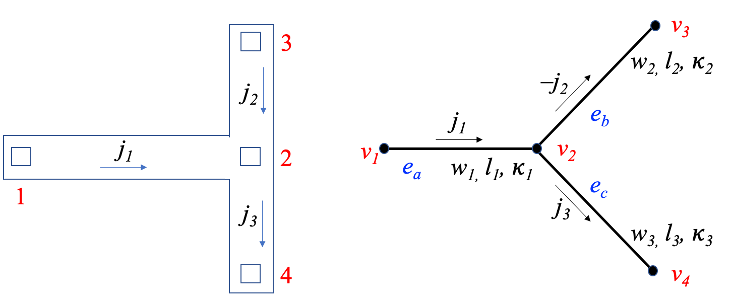
Along each edge, we use a local coordinate system along each segment . If the edge has a reference direction from node to node , we represent the position of node as and that of node as . As part of our analysis, we will compute stresses induced within the interconnect. Specifically,
- •
is the stress within wire segment at time at a location , where and .
- •
is the steady-state stress at node , .
II-B Stress equations for interconnect structures
A single interconnect segment injects electron current at a cathode at towards an anode at . The temporal evolution of EM-induced stress, , in the segment is modeled as [10]:
| (1) |
Here, is the distance from the cathode and is the time for which the wire was stressed and is the current density through the wire. The term , where is the effective charge number, is the electron charge, is the metal resistivity, and is the atomic volume for the metal (in the literature, is often denoted as ). The symbol , where is the diffusion coefficient, is the bulk modulus of the material, is Boltzmann’s constant, and is the absolute temperature. Further, where is the activation energy.
When no current is applied, the stress in the wire is given by , the thermally-induced stress due to differentials in the coefficient of thermal expansion (CTE) in the materials that make up the interconnect stack. The differential equation with the boundary conditions can be solved numerically to obtain the transient behavior of stress over time. Due to superposition, the stress in the wire can be computed in this way and can then be added to account for CTE effects. The impact of is to offset the critical stress, , to .
As in [10], the sign convention for is in the direction of electron current, i.e., opposite to the direction of conventional current and the electric field. The atomic flux attributable to the electron wind force is proportional to the second term on the right hand side that contains , while the flux related to the back-stress force is proportional to the first term containing the stress gradient . In both cases, the constant of proportionality varies linearly with the cross-sectional area of the wire. The sum, , is proportional to the net atomic flux.
BCs for single-segment interconnect When electron current is injected through the anode and flows to the cathode at the other end, we have zero-flux conditions at each end:
| (2) |
BCs for a multisegment interconnect trees/meshes The boundary conditions at the terminus nodes (i.e., nodes of degree 1) require zero flux across the blocking boundary, i.e.,
| (3) |
where edge connected to the terminus has current density .
For any internal node of the structure with degree , let the incident edges with reference current directed into the node be , and the edges directed away from the node be ; if either set is empty, or . The flux boundary conditions at such a node are given by
| (4) | ||||
and the continuity boundary conditions are:
| (5) |
where and are the values of the stress and its derivative at the location corresponding to node .
III Intuitive Explanation
Explanations of electromigration are often mired in the solutions of the partial differential equations presented in the previous section. In this section, we present an intuitive view of the solution of the steady-state problem, which helps easier understanding of the material in the succeeding sections.
It is well known that in the steady state, after all transients have dissipated, the stress varies linearly along a wire, and the gradient of the stress is proportional to the current density in a wire (we will show in Eq. (6) that for a wire with current density , this slope is ), and that the stress function is continuous at segment boundaries (Eq. 5). Given these two facts, the stress profile for a three-segment line is as shown in Fig. 3, where the steady-state stress at vertex is , for , and the slope of each segment is proportional to the current density in the segment; note that the sign of the slope in the middle segment is the opposite to that in the other segments since the direction of current flow is also the opposite to other segments.

Therefore, if we knew , the other stress values could be computed based on the known slopes: is lower than by ; is higher than (due to the change in current direction) by ; and is reduced from by . In other words, given all values, all stresses may be written in terms of as shown in the figure (as we will show later, this is equally true for tree structures and meshes), where the values of depend on the currents in the lines.
To find , we simply appeal to the concept of conservation of mass: although atoms are transported along the wire, there is no change in the total number of atoms in the wire due to EM. For wires of equal width and thickness, as in this example, this translates to a condition (Lemma 3) that the integral of stress over the region is zero. Since all values are expressed in terms of , this integral depends purely on : equating it to zero provides , and therefore, .
We develop this intuition to a formal set of results in this paper. We present two solutions for stress computation:
- •
A current-desnity-based approach that traverses all segments – in this case, from to – to find the “drop” along each segment to compute the stress value at each vertex. Combining this with the mass conservation equation, this provides the steady-state stress at each node.
- •
A voltage-based formulation where stress computation is traversal-free – by showing that since the “drop” along a segment is proportional to the IR drop along the segment, we point out that the traversal has already been implicitly performed during circuit simulation, which computes all voltages (and currents) in the system. Therefore, since (modified) nodal simulation of the network is essential to predict the currents through the wires, we show that the steady-state stress at each node can be computed by eschewing any traversal during EM analysis, and instead, reusing the steady-state voltages.
Both solutions have a cost that is linear in the number of segments in the circuit, though the latter method has a lower constant of proportionality for the linear-time complexity since it can be performed without traversals.
We also prove that the EM analysis for mesh-based structures merely needs the analysis of a spanning tree of the mesh, thus making steady-state EM analysis of meshes simple.
IV Analysis of Steady-state Stress
IV-A Equations for steady-state analysis in a wire segment
We will work with (1) as a general representation of the stress in any multisegment line or tree. In the steady state, when the electron wind and back-stress forces reach equilibrium, then for each segment , over its entire length, ,
| (6) |
The Blech criterion for immortality in a single-segment line asserts that in the steady state, if the maximum stress falls below the critical stress, , required to nucleate a void, then the wire is considered immortal, i.e., immune to EM. This translates to the condition [1]:
| (7) |
where is a function of the critical stress, .
The derivation of the Blech criterion is predicated on the presence of blocking boundary conditions at either end of a segment carrying constant current, and is invalid for multisegment wires, even though it has been (mis)used in that context. For a general multisegment structure, from (6), a linear gradient exists along each segment of a general multisegment structure (this has been observed for multi-segment lines [14, 15] and meshes [20]).
Lemma 1: For edge with reference current direction from vertex to , the steady-state stress along the segment is:
| (8) | ||||
| (9) |
where () denotes the steady-state stress at node ().
Proof: The first expression follows directly from (6), and the second is obtained by substituting at node .
The following corollary follows directly from (8):
Corollary 1:
For edge in an interconnect structure,
| (10) |
Corollary 2: In a segment, the largest stress is at an end point.
Proof: This follows from (9): if , the stress on the segment is maximized at node ; otherwise at node .
IV-B Equations for steady-state analysis in a general structure
The existence of cycles in a graph requires careful consideration: we show that the solution can be found by analyzing a spanning tree.

Theorem 1: Consider any undirected simple cycle, without repeated vertices or edges, in , consisting of edges containing vertices , with edge reference directions from to (where ), as shown in Fig. 4. The steady-state stress equations (9) representing this cycle are linearly dependent. A linearly independent set of equations is obtained by dropping one equation, i.e., breaking the cycle by dropping one edge.
Proof: Let be the voltage at vertex , be the resistance of wire segment , be the wire resistivity, and be the wire thickness (constant in layer ). Then and by Ohm’s law, the electron current is given by:
| (11) |
According to (9), along each edge ,
| (12) |
Adding up all equations (12) around the cycle, the left hand side sums up to zero, because each term in one equation has a corresponding term in the next equation (modulo , so that and appear in the last and first equation, respectively). Similarly, the right-hand side also sums up to zero due to telescopic cancelations of in each equation and in the next equation (modulo ).
Therefore, the equations (12) are linearly dependent. They can be represented by equations: by breaking the cycle at an arbitrary position and removing one edge, the simple cycle is transformed to a path with a set of independent linear equations.
The implications of Theorem 1 are profound, namely:
The steady-state stress in any structure with cycles can be solved by
removing edges to make it acyclic, yielding a spanning tree structure, which is
then solved to obtain the stress at all nodes.
IV-C Solving the steady-state analysis equations
We will first analyze a tree structure, since, as shown above, the steady state difference equations (9) are to be solved over a spanning tree of a general interconnect structure.
We choose an arbitrary leaf node of the tree as a reference; without loss of generality, we will refer to it as node , and the stress at that node as . For any node in the tree, there is a unique directed path from to , where each edge has a direction from to where is the vertex that is closer to . Note that edges on this path are directed from towards . However, it is built on an undirected graph for the tree, where each undirected edge of the tree has a reference current direction.
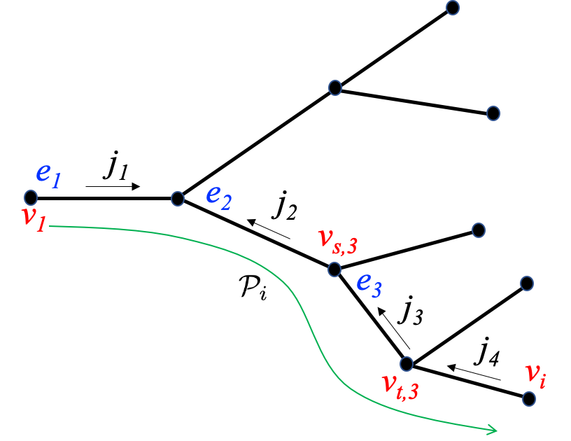
To illustrate this point, consider the tree in Fig. 5, with path from vertex to . Vertex is the vertex of that is closer to . The reference current directions on the undirected graph are as shown: the direction of is along the direction of path , while , , and are in the opposite direction.
Definition: We define , the “Blech sum” for a path , as:
| (13) |
where the summation is carried out over all edges on path . The term if the reference current direction for edge is in the same as path ; otherwise, . Informally, is the algebraic sum along from to .
In the example of Fig. 5, the Blech sum to is
Lemma 2: The stress, at node is related to as follows:
| (14) |
Proof: In a tree, the path must be unique [29]. Along this path, the current on each edge from to is , i.e., if the reference current direction is from to , and otherwise. Therefore, from (9),
| (15) |
The continuity boundary condition (5) ensures that the stress at the distal end of an edge on is identical to that on the proximal end of its succeeding edge, i.e., for successive edges and on , . Therefore, adding these equations over all edges on path , we see that as successive edges on the path share a vertex , cancels out telescopically, except for or . Meanwhile, the terms add up, so that the sum of all equations yields
| (16) |
This leads to the result in (14).
However, (14) in Lemma 2 stops short of determining at each node: for a tree with nodes, the lemma provides () linear equations in variables, leading to an underdetermined system where each node stress is related to the stress, , at an arbitrarily chosen leaf node, . The equation is obtained from the principle of the conservation of mass: atoms are transported along a wire, but with zero net change in the number of atoms in the wire.
Lemma 3: For a general tree/mesh interconnect with edges, with edge having width and height ,
| (17) |
Proof: The stress on a wire segment causes a displacement of in segment of the interconnect structure. The stress has no shear component since the current in a line is unidirectional. Due to conservation of mass, the net material coming from all wire segments is zero, and therefore,
| (18) |
where is the width of the wire segment. The displacement is the integral of displacements over the segment caused by stress applied on elements of size in segment . If is the bulk modulus, from Hooke’s law,
| (19) |
Combining this with (18) leads to the result of Lemma 3. In effect, this result is an integral form of the BCs (4), which conserve flux at the boundary of each segment in the tree.
Theorem 2: A tree or mesh interconnect with edges and vertices is immortal when:
| (20) | ||||
| (21) |
where is the “Blech sum” defined in (13).
Proof: We first show that expression (21) provides the stress at node of the interconnect, and is obtained by combining the result of Lemma 3 with the equations from (14).
Let edge connect vertices and , where is the vertex that is closer in the tree to the reference node . Then, substituting the result of Lemma 2 into Corollary 1,
| (22) |
where is the Blech sum from node to node .22 2 The use of allows for the traversal from to to include edges in a direction opposite to the reference current direction: the stress difference between nodes on such edges should have the opposite sign as (9) in Lemma 1.
Substituting the integral expressions in (17) from Lemma 3:
| (23) |
After further algebraic manipulations, we obtain
| (24) |
Finally, we substitute the above into (14) to obtain (21), the expression for the steady-state stress values at each node .
For the interconnect to be immortal, the largest value of stress in the tree must be lower than , the critical stress required to induce a void. From Corollary 2, in finding the maximum stress in the tree, it is sufficient to examine the stress at the nodes of the tree, so that the largest node stress is below . This proves (20).
V Linear-Time Immortality Calculation Based on a Current Density Formulation
As we have established, a general interconnect on a graph can be solved by considering the solution of Theorem 1 on a tree of the graph. Identifying such tree is straightforward, and standard methods such as depth-first or breadth-first traversal can be used.
After arriving at a tree structure, although Theorem 2 provides a useful, closed-form result, a simple-minded computation would calculate at each node in the tree through repeated incantations of (21). However, as we will show, this computation can be performed in time for a structure with edges. We rewrite (21) as:
| (25) | ||||
| (26) | ||||
| (27) |
This computation requires the calculation of three summations for , , and for the Blech sum, from reference node to each node in the tree. It proceeds in the following steps:
- 1.
To compute , we traverse the tree from using a standard traversal method, e.g., the breadth-first search (BFS). At node , we initialize . As we traverse each edge , we compute .
- 2.
- 3.
Finally, we compute at each node using (25).
If the stress at each end of a segment is below , it is immortal. If not, it is potentially mortal and is further analyzed using a transient stress analysis method [3, 13, 4, 5, 6, 24, 25] to determine its stress value at the end of the chip lifetime.
Complexity analysis: The BFS traversal in Step 1 over a tree traverses edges. For each edge, Step 2 performs a constant number of computations to obtain and ( (27)–(26)). The final computation of (25) in Step 3, and the immortality check that compares the computed value with according to (20), perform a constant number of computations for nodes. Therefore, the computational complexity is .

Example: We illustrate our computation for a two-segment line (Fig. 6) in a single layer (with constant ) in Table I, using the leftmost node as the reference. Starting from , the two edges are traversed to compute . The symbol represents the Blech sum calculated at the distal vertex of the edge; note that the computation of uses the Blech sum at the proximal vertex, .
| Initialization | 0 | 0 | 0 |
| Edge | |||
| Edge | |||
VI An Alternative Voltage-Based Formulation
In a typical design flow, an interconnect system is analyzed via circuit simulation to determine currents and voltages throughout the system. For example, for a power delivery network, which is the most critical on-chip interconnect system that requires EM analysis, a system of nodal or modified nodal equations is solved to obtain voltages throughout the network, and currents are then inferred from the (modified) nodal formulation. In this section, we will show how an immortality check can be performed using the computed nodal voltages, without the need for any traversals during stress computation.
We begin by introducing a result that relates the drop along a segment to the voltage drop across it.33 3 This result can also be a powerful tool in formulating power grid optimization problems. To ensure that EM constraints in a grid are met, it is sufficient to ensure that the steady-state EM stress (which is a sum of terms) does not exceed . Given this direct relationship between EM and IR drop constraints, it is possible to formulate a power grid optimization problem that ensures EM-safe power grids while working entirely within the space of voltage variables.
Lemma 4: Consider a wire connecting nodes and , with resistance , resistivity , and length . If the current density in the wire is , in the direction of electron current, then
| (29) |
where and are the voltages at endpoints and of the wire. Note that this mirrors the second inequality in Eq. (12).
Proof: If the conventional current in the wire is and its cross-sectional area is , then
| (30) |
The second equality arises from the relation . The negative sign arises because is in the direction of electron current while is in the direction of conventional current.
Corollary 3: Consider a path with edges and nodes with node voltages , respectively. The Blech sum along this path is
| (31) |
The proof of this corollary is trivial, and arises through the application of Eqs. (13) and (29): along a path, the voltages of all intermediate nodes telescopically cancel, leaving the first and last nodes of the summation as shown in the result.
Theorem 3: Given the voltages at each node in any interconnect system (tree or mesh), the EM-induced stress at node in any interconnect system (tree or mesh), is given by
| (32) |
where is the voltage at node and is the average of the voltages at the two terminals of the segment represented by .
Proof: We rewrite from (26) using voltage variables. For an arbitrarily chosen vertex whose node voltage is , and which has a path to the vertex represented by node ,
| (33) |
where is defined in Eq. (27). From Eqs. (25), (31), and (33),
This leads to the following traversal-free DC stress computation procedure:
- 1.
For each edge in the circuit, we compute as the mean of the voltages at its two ends in time.
- 2.
Over all edges in the circuit, we compute in time.
- 3.
Next, we compute using Eq. (27), summing over all edges, also in time.
- 4.
Finally, we compute at each node using (32), given , in time.
Complexity analysis: Clearly, the cost of the computation is , including final immortality check that compares the computed value with , requires time.
It is easily verified that our approach results in the same solution for the example in Fig. 6 as listed in Table I.
A similar voltage-based result has been derived in [30] (the precise equations have some differences but can be shown to be equivalent), but its potential for linear-time computation was never realized as it was applied to a set of very small test structures. This formulation was used again in [23], and applied to a wider set of structures, however, their results show a quadratic to cubic growth in runtime with problem size, and it was apparently not noticed that such an approach can yield a linear-time solution for any arbitrary interconnect, as is shown in this paper. Moreover, although [23] applied the technique to mesh structures, neither their proof nor that in [30], on which the work was based, theoretically demonstrates that this extension to meshes is valid. In constrast, our work proves the validity of this method on mesh structures through Theorem 1.
VII Comparison with the
Via Node Vector Method
In [19], the two-segment structure of Fig. 6 was experimentally analyzed, with a current density of and , , and . It was observed that the time-to-failure of the segment with the lower current density was shorter, apparently contradicting the conventionally held belief that segments with the highest current are the most vulnerable to EM. The discrepancy was explained by correctly stating that the underlying cause is that Segment 1 provides atomic flux to Segment 2, leading to higher depletion at its cathode.

However, the difference in the time-to-failure between the two segments was corrected only heuristically by stating that for flux purposes, Segment 1 has an “effective” current of , corresponding to its own flux and the flux supplied to Segment 2. The “effective” current on Segment 2 is conjectured to be , accounting for the current of supplied by Segment 1. Based on this, and the observed superlinear behavior of electromigration time-to-failure (TTF), it was conjectured that a 3 factor between the effective currents of and on the two segments, which leads to a 3 stress differential, could explain the difference in the time to failure. However, in a Black’s equation framework, this would lead to an exponent of to explain the 10 discrepancy in the TTFs.
If the proposed effective currents are applied to the segments independently, the corresponding stress waveforms are as shown in Fig. 7(a). This is clearly incorrect since it does not satisfy the basic requirements of stress continuity at vertex . A more exact analysis of the steady-state flux can be performed applying Equation (28), with and , to compute the peak steady-state stress in Segment 1 and Segment 2 as:
| (34) | ||||
The corresponding stress waveforms, which are correct according to the underlying physics, are shown in Fig. 7(b). The peak stress on Segment 1 is actually 5 that of Segment 2. Translating this back into an “effective” current, this implies that the effective current is 5 larger in Segment 1. For a 10 difference in TTF, this leads to a more conventional exponent for in Black’s equation of 1.4, lying between the generally accepted range of 1 and 2.


VIII Results
We present three sets of results. We first compare our approach with a numerical solver in Section VIII-A on a simple mesh structure. Next, we apply our current-density-based and voltage-based approaches to the large public-domain IBM power grid benchmarks in Section VIII-B. Finally, in Section VIII-C, we perform an analysis on more modern nodes: commercial 12nm FinFET and 28nm FDSOI nodes, and an open-source 45nm technology, all based on Cu DD interconnects. We implement both our voltage-based and current-density-based analyses in Python3.6 and apply them to the benchmarks.
Although our method can be applied to interconnect structures built using any materials, we use modern Cu DD technologies in our evaluations. In particular, since the IBM benchmarks were originally designed for Al interconnects, a technology that is now obsolete, we use the topologies from this benchmark set and assume the interconnect to be built with Cu DD wires. In Cu DD interconnects, each layer can be treated separately due to the presence of barrier/capping layers that prevent atomic flux from flowing across layers through vias [27, 28]. The methods in this paper are applied to each layer to find the steady-state stress, which is then used to predict immortality. This limits the size of the EM problem, since it must be solved in a single layer at a time. Moreover, since it is common to use a reserved layer model where all wires in a layer are in the same direction [31], effectively this implies that each layer consists of a set of metal lines with a limited number of nodes. In such scenarios, the EM problem reduces to the analysis of a large number of line/tree structures. However, our method is also exercised on the IBM benchmarks, which contain mesh structures within layers, allowing for full evaluation of the generality of our method.
VIII-A Comparison with COMSOL
We show comparisons between our approach and numerical simulations using COMSOL on Cu DD structures. The material parameters, provided to COMSOL, are [16]: 2.25e-8m, 28GPa, 1.18e-29m3, 1.3e-9m2/s, 0.8eV, 1, MPa, K. Note that since , the constant used in Eq. (32) of the voltage-based formulation is .
COMSOL is limited to analyzing small structures, which is reflected the topologies shown in Fig. 8:
- •
An interconnect tree with three segments
- •
A larger interconnect tree
- •
A simple mesh structure
The color maps in the figure show the spatial variation of steady-state stress over each interconnect. The numbers next to each node represent the values computed using our approach and by COMSOL. The numbers match well; our approach is exact, and the small discrepancies are due to numerical inaccuracies in COMSOL, e.g., due to discretization.
VIII-B Analysis on IBM power grid benchmarks
The only widely used power grid benchmark suite is the set of IBM benchmarks [32]. Each benchmark contains Vdd and Vss networks and multiple voltage domains, and general tree/mesh structures in individual layers. We use SPICE to obtain the branch current and node voltages. For these benchmarks, we use two approaches for stress computations (i) a current-density-based traversal as explained in Section V, and (ii) a voltage-based approach as explained in Section VI.
The IBM power grid benchmarks are available as SPICE netlists and do not specify widths and thicknesses of segments in the grid. Therefore, we back-calculate the product of the width and thickness (cross-sectional area) of each segment such that, in consistency with Eq. (30), the remains constant within a metal layer, i.e., the cross-sectional area of the segment is the reciprocal of the resistivity.
We implement a BFS traversal over these structures using Python3.6 and Deep Graph Library [33] by modifying the message passing functions. For both approaches, a single traversal is required to find the connected components in the graph, on which the computations are carried out. For the current-density-based formulation, a BFS traversal is used to compute the stress value at every node, while the voltage-based formulation computes the stress at every nodes using (32) without a traversal. We report the runtimes on a 2.2GHz Intel Xeon Silver 4114 CPU for both approaches.

The traditional Blech criterion is only accurate for a single-segment wire: next, we evaluate its accuracy. We consider our approach as the accurate result since it is rigorously derived for multisegment structures by generalizing the same physics-based modeling framework used by the Blech criterion for one-segment wires, and it is validated on COMSOL. Therefore a positive identification of immortality implies that our method finds the segment to be immortal; a negative identification implies mortality. Fig. 9 plots the current density vs. the wire length within the segments of the ibmpg6 benchmark44 4 The figure shows the 1.6M edges of the ibmpg6 benchmarks. The scatter points of several segments may be hidden due to overlaps.. The currents in the Vdd and Vss lines may be either positive or negative, and their magnitude affects EM. The black triangles show the contours of : when the magnitude lies within this frontier for a segment of the grid, the traditional Blech criterion (7) would label the wire as immortal; otherwise it is potentially mortal. To help highlight erroneous predictions, the figure shows green markers for correct predictions and red markers for incorrect predictions. The Blech criterion shows significant inaccuracy on multisegment wires.
| TP | TN | FP | FN | Runtime (s) | |||
| J-based | V-based | ||||||
| pg1 | 29750 | 7788 | 7432 | 9079 | 5451 | 6.8 | 4.0 |
| pg2 | 125668 | 44564 | 18943 | 45224 | 16937 | 17.6 | 9.5 |
| pg3 | 835071 | 481604 | 4328 | 346322 | 2817 | 119.4 | 80.6 |
| pg6 | 1648621 | 1173842 | 177 | 473122 | 1480 | 243.66 | 150.3 |
We compare the predictions of the traditional Blech criterion against the ground truth, which corresponds to the provably correct analysis from our method. True predictions (true positive (TP) and true negative (TN)) correspond to correct predictions where the Blech criterion agrees with our accurate analysis; otherwise the predictions are false (false positive (FP) and false negative (FN)). A positive prediction from the Blech criterion implies that a segment is immortal; a negative prediction indicates a mortal segment. The errors correspond to false negative predictions, where a truly immortal segment is deemed potentially mortal by the traditional Blech criterion, and FPs, where a mortal segment is labeled as potentially immortal by Blech. False positives cause failures to be overlooked, and false negatives may lead to overdesign as EM-immortal wires are needlessly optimized. Table II summarizes the results on IBM benchmarks55 5 We do not show the numbers for pg4 and pg5 as we find all segments in these benchmarks to be immortal in our experiments.. The table shows that:
- •
the inaccuracies in the traditional Blech filter are not isolated but are seen across benchmarks.
- •
our method is scalable to large mesh sizes with low runtimes.
From the data, it is apparent that the traditional Blech criterion can provide misleading results. The reasons for this are:
- •
A high- segment could be immortal if it has numerous downstream segments with low , so that the total sum may be low. For example, in Fig. 6, if the current density , then the segment acts as passive reservoir, bringing down the stress in the right segment to be lower than the case of an identical isolated segment carrying the same current, but with a blocking boundary at [22].
- •
A low- segment could be labeled immortal by the traditional criterion, but it may be mortal due to a high stress at one node, caused by a high Blech sum for downstream wire segments, which could raise the stress at the other node.
We verify that our voltage-based and current-based formulations are identical by comparing the computed stress values for all segments in the IBM benchmarks. For example, Fig. 10 shows a scatter plot of the stress values for all segments in the ibmpg1 benchmark where the x-axis has the stress values computed by the current-density-based approach and y-axis shows the stress value of the segments computed by the voltage-based approach. The mean error is 18pPa and the maximum error is less than 60pPa. These negligibly small errors can be attributed to numerical precision issues.
The TP, TN, FP, and FN values in Table II are identical between our equivalent voltage-based and current-density-based approaches. The table shows that the voltage-based approach is 1.5–1.9 faster than the current-density-based approach as it does not require traversals for stress computation.66 6 We do not include the runtimes for parsing the benchmark files as modern design flows work with databases where power grid nets and wires can be queried in negligible time.
VIII-C Analysis on OpenROAD power grids
In this section, we show simulations based on power grids from circuits designed using a commercial 12nm FinFET technology, a 28nm technology, and an open-source 45nm technology using Cu DD interconnects. The circuits are taken through synthesis, placement, and routing in these technology nodes (some circuits are implemented in both nodes) using a standard design flow. The power grid is synthesized using an open-source tool, OpeNPDN [34] from OpenROAD. The IR drop and currents are computed using PDNSim [35]. Since the standard cell rows in the OpenROAD benchmarks have low utilizations, the current densities in the chip are low. Therefore, to evaluate our method, we scale the branch currents such that there are tens of mortal segments in each design.77 7 In principle, the same effect would be achieved with a sparser power grid, with larger IR drops, and therefore larger values, i.e., larger Blech sums that translate into more EM failures.
Fig. 11 shows a scatter plot that analyzes the inaccuracy of the traditional Blech criterion on a Cu DD technology, using A/m, based on material parameters listed in Section VIII-A. Due to the regular structure of the power grid, many lines have the same length. As in the earlier case, it is easily seen that the Blech criterion leads to numerous false positives and false negatives. Results for more circuits are listed in Table III and show similar trends. The number of mortal segments as per Blech criterion, i.e., true negatives and false negatives is small across all benchmarks and technologies. This is attributed to the fact that values are small as compared to ibmpg benchmarks. However, there are significant numbers of false positives across all benchmarks, which indicates the inaccuracy of the traditional Blech filter, when misused for multisegment wires. For these testcases, the voltage-based solution is 1.7–2.7 faster than the current-density-based solution.
| Circuit | TP | TN | FP | FN | Runtimes (s) | |||
| J-based | V-based | |||||||
| 12nm | gcd | 4,121 | 2,177 | 94 | 1,821 | 29 | 0.9 | 0.5 |
| jpeg | 83,743 | 50,436 | 5 | 33,250 | 52 | 10.6 | 6.2 | |
| dynamic_node | 150,768 | 79,990 | 0 | 70,757 | 21 | 17.9 | 9.5 | |
| aes | 194,485 | 84,132 | 0 | 110,330 | 23 | 23.3 | 12.3 | |
| 28nm | gcd | 678 | 400 | 70 | 158 | 50 | 0.4 | 0.2 |
| aes | 11,361 | 4,946 | 62 | 5,862 | 491 | 2.9 | 1.6 | |
| 45nm | dynamic_node | 6,610 | 4,943 | 0 | 1,641 | 26 | 1.2 | 0.6 |
| aes | 7,996 | 5,562 | 2 | 2,393 | 39 | 1.9 | 0.7 | |
| ibex | 12,723 | 9,273 | 0 | 3,438 | 12 | 1.8 | 0.8 | |
| swerv | 61,935 | 43,122 | 0 | 18,810 | 3 | 7.4 | 4.0 | |
Next, we show the stress profile in a single power stripe of length 999m from the aes benchmark, synthesized in a commercial 12nm technology. The line consists of 185 segments, each carrying different currents. The stress profile is shown in Fig. 12: due to the large number of segments in the line, the profile may appear nonlinear at this resolution, but the steady-state stress in each segment is linear along its length, and the stresses obey continuity at the segment boundaries, as specified by the boundary conditions. The figure shows excellent agreement between our analysis and a COMSOL simulation. However, COMSOL must solve the transient stress problem for a long period before the steady state is achieved, while our approach provides the solution in milliseconds.
IX Conclusion
This work proposes a theoretically justified method for checking immortality in a general tree or mesh interconnect. The theoretical basis for the method is presented, and two versions – a current-density-based method and a voltage-based approach – are presented. Although not elaborated upon in this work, the voltage-based formulation is potentially useful for power grid optimization, since it translates EM constraints into IR constraints, enabling a unified formulation that optimizes a power grid for both IR drop and EM, while operating purely in the realm of voltages (i.e., translating stress variables to voltage variables). Both the current-density-based and voltage-based approaches have linear time complexity, the latter is, on average, 1.9 faster than the former. The results are validated against COMSOL and it is shown that the methods are fast and scalable to large power grids.
References
- [1] I. A. Blech, “Electromigration in thin aluminum films on titanium nitride,” J. Appl. Phys., vol. 47, no. 4, pp. 1203–1208, 1976.
- [2] J. R. Black, “Electromigration failure modes in aluminum metallization for semiconductor devices,” Proc. IEEE, vol. 57, no. 9, pp. 1587–1594, 1969.
- [3] H.-B. Chen, et al., “Analytical modeling and characterization of electromigration effects for multibranch interconnect trees,” IEEE T. Comput. Aid D., vol. 35, no. 11, pp. 1811–1824, 2016.
- [4] S. Chatterjee, et al., “Power grid electromigration checking using physics-based models,” IEEE T. Comput. Aid D., vol. 37, pp. 1317–1330, July 2018.
- [5] V. Mishra and S. S. Sapatnekar, “The impact of electromigration in copper interconnects on power grid integrity,” in Proc. DAC, pp. 88:1–88:6, 2013.
- [6] V. Mishra and S. S. Sapatnekar, “Predicting electromigration mortality under temperature and product lifetime specifications,” in Proc. DAC, pp. 43:1–43:6, 2016.
- [7] R. Rosenberg and M. Ohring, “Void formation and growth during electromigration in thin films,” J. Appl. Phys., vol. 42, no. 13, pp. 5671–5679, 1971.
- [8] M. Schatzkes and J. R. Lloyd, “A model for conductor failure considering diffusion concurrently with electromigration resulting in a current exponent of 2,” J. Appl. Phys., vol. 59, pp. 3890–3893, 1986.
- [9] J. J. Clement and J. R. Lloyd, “Numerical investigations of the electromigration boundary value problem,” J. Appl. Phys., vol. 71, pp. 1729–1731, 1992.
- [10] M. A. Korhonen, et al., “Stress evolution due to electromigration in confined metal lines,” J. Appl. Phys., vol. 73, no. 8, pp. 3790–3799, 1993.
- [11] M. Ohring and L. Kasprzak, Reliability and Failure of Electronic Materials and Devices. Cambridge, MA: Academic Press, 2nd ed., 2011.
- [12] V. Sukharev, “Beyond Black’s equation: Full-chip EM/SM assessment in 3D IC stack,” Microelectronic Engineering, vol. 120, pp. 99–105, 2014.
- [13] H.-B. Chen, et al., “Analytical modeling of electromigration failure for VLSI interconnect tree considering temperature and segment length effects,” IEEE T. Device Mater. Rel., vol. 17, no. 4, pp. 653–666, 2017.
- [14] S. P. Riege, et al., “A hierarchical reliability analysis for circuit design evaluation,” IEEE T. Electron Dev., vol. 45, pp. 2254–2257, Oct. 1998.
- [15] J. J. Clement, et al., “Methodology for electromigration critical threshold design rule evaluation,” IEEE T. Comput. Aid D., vol. 18, pp. 576–581, May 1999.
- [16] S. M. Alam, et al., “Circuit-level reliability requirements for Cu metallization,” IEEE T. Device Mater. Rel., vol. 5, no. 3, pp. 522–531, 2005.
- [17] D. Li, et al., “T-VEMA: A temperature- and variation-aware electromigration power grid analysis tool,” IEEE T. VLSI Syst, vol. 23, no. 10, pp. 2327–2331, 2015.
- [18] A. Abbasinasab and M. Marek-Sadowska, “Blech effect in interconnects: Applications and design guidelines,” in Proc. ISPD, pp. 111–118, 2015.
- [19] Y. J. Park, et al., “New electromigration validation: Via node vector method,” in Proc. IRPS, pp. 698–704, 2010.
- [20] H. Haznedar, et al., “Impact of stress-induced backflow on full-chip electromigration risk assessment,” IEEE T. Comput. Aid D., vol. 25, pp. 1038–1046, June 2006.
- [21] M. H. Lin and A. S. Oates, “An electromigration failure distribution model for short-length conductors incorporating passive sinks/reservoirs,” IEEE T. Device Mater. Rel., vol. 13, pp. 322–326, Mar. 2013.
- [22] M. H. Lin and A. S. Oates, “Electromigration failure of circuit interconnects,” in Proc. IRPS, pp. 5B–2–1–5B–2–8, 2016.
- [23] Z. Sun, et al., “Fast electromigration immortality analysis for multisegment copper interconnect wires,” IEEE T. Comput. Aid D., vol. 37, pp. 3137–3150, Dec. 2018.
- [24] B. Li, et al., “Statistical evaluation of electromigration reliability at chip level,” IEEE T. Device Mater. Rel., vol. 11, pp. 86–91, Mar. 2011.
- [25] M. A. A. Shohel, et al., “Analytical modeling of transient electromigration stress based on boundary reflections,” in Proc. ICCAD, 2021.
- [26] M. A. A. Shohel, et al., “A new, computationally efficient ‘Blech criterion’ for immortality in general interconnects,” in Proc. DAC, 2021.
- [27] J. Gambino, “Process technology for copper interconnects,” in Handbook of Thin Film Deposition (K. Seshan and D. Schepis, eds.), ch. 6, pp. 147–194, Amsterdam, The Netherlands: Elsevier, 3rd ed., 2018.
- [28] L. Zhang, et al., “Grain size and cap layer effects on electromigration reliability of Cu interconnects: Experiments and simulation,” in AIP Conf. Proc., vol. 1300, 3, 2010.
- [29] T. H. Cormen, et al., Introduction to Algorithms. Boston, MA: MIT Press, 3rd ed., 2009.
- [30] E. Demircan and M. Shroff, “Model based method for electro-migration stress determination in interconnects,” in Proc. IRPS, pp. IT5.1–IT5.6, 2014.
- [31] T. Jhaveri, et al., “Co-optimization of circuits, layout and lithography for predictive technology scaling beyond gratings,” IEEE T. Comput. Aid. D., vol. 29, pp. 509–527, Apr. 2010.
- [32] “IBM power grid benchmarks.” https://web.ece.ucsb.edu/~lip/PGBenchmarks/ibmpgbench.html, Accessed November 20, 2020.
- [33] M. Wang, et al., “Deep graph library: A graph-centric, highly-performant package for graph neural networks,” in arXiv:1909.01315 [cs.ar], 2020.
- [34] V. A. Chhabria, et al., “Template-based PDN synthesis in floorplan and placement using classifier and CNN techniques,” in Proc. ASP-DAC, pp. 44–49, 2020.
- [35] V. A. Chhabria and S. S. Sapatnekar, “PDNSim.” github.com/The-OpenROAD-Project/OpenROAD/tree/master/src/PDNSim.