Quantitative infrared near-field imaging of suspended topological insulator nanostructures
Abstract
The development of nanoscale solid-state devices exploiting the promising topological surface states of topological insulator materials requires careful device engineering and improved materials quality. For instance, the introduction of a substrate, device contact or the formation of oxide layers can cause unintentional doping of the material, spoiling the sought-after properties. In support of this, nanoscale imaging tools can provide useful materials information without the need for complex device fabrication. Here we study Bi2Se3 nanoribbons suspended across multiple material stacks of SiO2 and Au using infrared scattering scanning near-field optical microscopy. We validate our observations against a multilayer finite dipole model to obtain quantitative imaging of the local Bi2Se3 properties that vary depending on the local environment. Moreover, we identify experimental signatures that we associate with quantum well states at the Bi2Se3 surfaces. Our approach opens a new direction for future engineering of nanoelectronic devices based on topological insulator materials.
Topological insulators (TIs) are an exciting class of materials that may find applications in a wide range of electronic and quantum devices, where their unique topologically protected surface states are exploited for new functionalities [1, 2]. However, synthesising materials and building practical devices remains a significant challenge. Much of this can be attributed to unintentional charge doping and defects in materials resulting in the bulk dominating the electron transport, and obscuring the topological surface contribution. In addition to intrinsic charge doping by impurities or vacancies, the position of the Fermi level will be influenced by the dielectric (substrate) material on which the TI material is located [3]. This issue is particularly relevant for thin TI materials, where the intrinsic bulk contribution is otherwise generally minimised by reduced dimensionality (’bulk-free’) [4, 5, 6, 7], and band bending will dope device surfaces differently [8, 3]. Selecting the right materials in connection to the TI is therefore important to fully exploit topological surface states. A particularly promising route for addressing this problem is the growth of single crystalline TI nanoribbons (TINRs) [9, 10]. These can easily be mechanically transferred to any substrate for further study and device fabrication[11]. Yet, device fabrication remains challenging, and obtaining transport data on a statistically relevant set of nanoribbons is very time consuming. To this end, rapid room-temperature scanning probe characterisation tools could aid in the search and characterisation of materials. Near-field optical microscopy techniques have recently emerged as effective probes of the doping of TI materials due to intrinsic defects [12, 13] and even as potential probes of the topological surface states [14]. Near-field microscopy is also a powerful tool to map surface plasmons expected to arise from the metallic TI surface states, with many applications in sub-wavelength optical devices[15, 16, 17, 18]. In all these cases, careful modelling of the dielectric environment of the TI material is key to quantitative imaging and extraction of material properties.
Here we combine scattering scanning near-field optical microscopy (sSNOM) with theoretical modelling using a finite-dipole model (FDM) extended to multiple dielectric layers to show that local electronic properties can be extracted in TINRs extending across multiple dielectric stacks, where different substrates can induce local variations in the TINR properties. We outline the methodology for quantitative evaluation of nanoribbon properties using sSNOM and demonstrate a route towards disentangling the impact of nanoribbon substrates on material properties by suspending the TINRs across multiple substrates.
We use Bi2Se3 TI nanoribbons grown on a glass substrate using the catalyst-free Physical Vapour Deposition (PVD) method outlined in Ref. [9]. The nanoribbons are mechanically transferred to a pre-patterned substrate consisting of multiple micron-sized trenches in SiO2, some with Au electrodes within. Further details can be found in the Supplemental Material (SM). We select to study a TINR that bridges several of these trenches. The cross-section of the sample and substrate is shown in Fig. 1a.

Measurements were carried out using a sSNOM operating at infrared wavelengths in combination with tapping-mode atomic force microscopy (AFM). The infrared near-field extends into a small volume underneath the tip, and the scattered radiation depends on the material properties in this volume. To minimise the contribution from far-field effects the collected signal is demodulated at the AFM cantilever oscillation frequency (330 kHz). We denote this signal by , where the subscript indicates the specific harmonic for demodulation. First, we consider surface scans obtained at different wavelengths of the infrared radiation. The AFM topography in Fig. 1b shows an 85 nm thick Bi2Se3 TINR suspended across trenches in SiO2, some with Au wires inside (note that there is always a small air gap between Au and Bi2Se3). Fig. 1c-d shows the corresponding sSNOM data for two selected wavelengths . In both cases, the Au is visible as vertical stripes with strong sSNOM response, and the SiO2 substrate shows almost negligible response despite significant topography variations across trenches. This indicates that the SiO2 is thick enough and for theoretical modelling purposes can be taken as the bottom-most (semi-infinite) layer. On the TINR significant contrast variations are observed when the Bi2Se3 is atop the Au stripes compared to a reduced signal when atop the SiO2 for cm-1 (Fig. 1c). Similarly, there is a significant difference when the TINR is suspended over the empty trenches. However, at cm-1 the Bi2Se3 appears almost homogeneous (Fig. 1d), with only a slightly stronger signal directly atop Au. Here only significant signal variations occurs in correspondence with the small dirt particles that causes the tip to be lifted from the Bi2Se3 surface, resulting in a reduced signal. These initial observations suggests that the measurement obtained by sSNOM is not exclusively dominated by the metallic gold wires, but it is sensitive to the different substrates along the nanoribbon, which may induce local variations in its properties. To provide a quantitative evaluation of the phenomena stemming from the multilayered sample, we use detailed modelling of the sSNOM response.

We model our system with a multilayer finite dipole model (MLFDM), first outlined in [19] and later discussed also in [20] and [21]. The geometry assumed in this model is shown in Fig. 2a. The tip is modelled by an elongated spheroid with length and tip apex radius . At the core of this model lies solving the image-charge problem as the illuminating IR radiation of amplitude excites an effective charge dipole, which is formed between tip and sample. Due to the dipoles formed by the charge-image charge pairs shown in Fig. 2a, the tip acquires an effective polarisability, which reads
| (1) |
where are the effective point charge positions and are their relative quasi-static electric coefficients. is a function of the tip geometry and is the tip sample distance with a static () and time-varying part with amplitude (see SM for further details). Evaluating is key in the numerical modelling, as the scattered near-field signal is proportional to . The signal is demodulated to minimise contributions from far-field effects and hence the quantity of interest is the complex-valued , arising from the Fourier transform of . In what follows we refer to the measured amplitude of the near-field response as the detected signal at the harmonic of . In general, detection at higher harmonics reduces the contribution from far-field effects. See the SM for a complete description of our model which takes into account up to 7 dielectric layers underneath the tip, sufficient to model Bi2Se3 bulk and surface states atop 3-layer substrates, as we have here in the case of Bi2Se3/Air/Au/SiO2.
To calibrate the response from the tip we measure a series of approach-curves and record the detected tip oscillation amplitude (Fig. 2b) together with the near-field response (Fig. 2c) on Au. We can distinguish three different regimes as function of : (i) non contact regime, characterised by an independent of . The point at which starts to decrease establishes the reference height, and sets the transition into what we here call the (ii) soft contact regime. Here the tip motion is damped due to its proximity with the sample, resulting in a modification of the harmonic content of the near-field response. Even closer to the sample the tip motion is further perturbed, which affects the near-field harmonics generation further, resulting in a saturated near-field response. We refer to the latter as the iii) hard tapping regime. Since the FDM model is defined under the assumption of a smooth sinusoidal oscillation of the tip-sample separation, benchmark between theory and measurements is exact for near-field values recorded in the non-contact regime, and valid at an approximate level in the soft-contact regime.
The geometrical properties of the tip (, , and a dimensionless parameter ), are then obtained through the fit of the model to the approach curves of a reference material (Au), with known optical properties. The approach curves in Fig. 2c show the behaviour of the second and the third harmonic of the near-field signal as a function of the tip-sample distance atop Au. We use Eq.1, with known dielectric function for Au [22], and we find that nm, nm, and gives good agreement across all measured wavelengths and harmonics. After calibrating the tip parameters on Au, the model is further validated against the response on SiO2 (see SM for further analysis).
We then proceed to extract the unknown dielectric function of the TINR located directly atop SiO2. To describe the optical response of the Bi2Se3 we use the Drude model, whose only free parameters are inverse scattering time and the plasma frequency , where is the carrier concentration and is the effective mass of bulk carriers in Bi2Se3[23]. Across wavelengths a good fit is obtained with cm-1 and cm-1, corresponding to cm-3. Fig. 2d shows an example of such a fit for varying at cm-1. This value for is in good agreement with what has been found in similar materials [24, 25], and only slightly higher than found via transport measurements of similar Bi2Se3 TINRs grown using the same process [8, 3], which is to be expected as device leads provides grounding and a reservoir for the carriers in the TINR.
To extract the Bi2Se3 properties we use the MLFDM, which takes into account the screening effect provided by the various dielectric layers underneath the tip. The effective positions of the image charges, introduced in Eq. 1, are a key indicator of this effect. As an example we consider two different cases: Bi2Se3/Air/SiO2 (Fig. 2e) and Bi2Se3/Air/Au/SiO2 (Fig. 2f). For Bi2Se3/Air/SiO2, the image charge shows a frequency dependent behaviour which bears similarities with the known dielectric response of SiO2. If a layer of Au is introduced in the air gap between Bi2Se3 and SiO2, the image charge position assumes a nearly constant behaviour as function of frequency, showing that even a thin layer of Au completely screens the effect of SiO2.

To get an insight into the optical properties of the TINR, we analyse the response at different frequencies of the irradiating field. The spectra shown in Fig. 3a and 3b, are obtained using two different measurement protocols. The first approach is based on the post processing of scans. The scans are obtained in what we here refer to as the soft tapping mode in terms of the near-field response, where the FDM is only approximately valid. Alternatively, spectra can be obtained from approach curves (Fig. 1d), where the near-field signal is available within a wide range of tip-sample distances, taken at specific locations on the sample. In both cases we investigate the local variation of the signal in the sample and we select the measurements recorded in four different positions corresponding to different material stacks (see Fig. 1b). Both measurements show a pronounced peak around cm-1, both atop the SiO2 and on top of the Bi2Se3. Across the entire frequency range considered, the strongest signal is obtained in the region where Au is below the Bi2Se3. A lower signal is measured when Bi2Se3 is in direct contact with the SiO2 layer, and the weakest signal is measured when an air gap is between Bi2Se3 and SiO2. To investigate the physical origin of the observed features, we compare the measurements with the MLFDM.
The model reproduces the peak at 1100 cm-1, from the dielectric response of the SiO2. The same signature is also obtained on the Bi2Se3, as a consequence of the presence of the SiO2 underneath the nanoribbon and a finite sampled near-field volume of size . The MLFDM also correctly predicts that the highest near-field response in the nanoribbon is recorded when Au is underneath. However, we also identify some discrepancies, which we address in what follows.
In Fig. 3c, it can be seen that the theoretical prediction of the near-field signal is not sensitive to the presence of an air gap between the Bi2Se3 and the SiO2 for cm-1, yet experimental data shows a clear difference between these two stacks, both from scans (Fig. 3a) and from approach-curve data (Fig. 3b). To differentiate the two predicted signals, we conducted a complete study of the role of the different parameters involved in the model. Importantly, the observed separation between the two MLFDM curves can only be reproduced when the nanoribbon’s plasma frequency is allowed to vary along its length, according to the materials below it. For a fixed this could only result from a varied carrier concentration (see Fig. S13 in SM for an extended analysis). This is expected to be the case, as different materials underneath may result in charge accumulation or depletion, depending on their work functions and properties of the interface [26, 8] and electrostatic effects. While not expected for pristine Bi2Se3 on SiO2[8], the higher observed in the case of Bi2Se3/Air/SiO2 could arise due to the presence of the Bi2Se3 surface oxide which modifies the work function alignment that occurs at the Bi2Se3/SiO2 interface[27]. The exact mechanism influencing the charge accumulation and depletion due to interfaces are still a matter of debate and subject to significant sample-to-sample variations, however, extensive sSNOM measurements could potentially shed more light on this issue. We note that within nanoribbons which are transferred onto a uniform substrate (bare SiO2), we do not observe any variations, implying a constant carrier concentration. This is in contrast to previous studies in other TI materials, where local variations were found in larger structures due to defects [20, 13]. Our results show that for Bi2Se3 nanoribbons placed across multiple substrate materials the situation can be different.
These observations are valid for cm-1. At and cm-1 we observe additional peaks in the experimental data (particularly pronounced in Fig. 3a), which are not captured by the Drude model, but can be phenomenologically captured (see SM Fig. S10) by adding Lorentz oscillators as additional surface layers in the MLFDM [14]. The presence of these peaks are not expected from any of the bulk materials involved in this system. They are also weakly seen atop SiO2, however, for higher harmonics, where far-field effects are suppressed, these peaks disappear (see Fig. S11 and S12). This implies that the peaks indeed originate from the Bi2Se3 itself. Similar features were observed in (Bi0.5Sb0.5)2Te3 [14], and are likely to originate from quantum well states (QWS) forming at the surfaces as a result of band-bending. Interestingly we observe two peaks of similar intensity, regardless of underlying substrate. It is therefore not likely that the two peaks originate from different QWS at top and bottom surfaces. Our simulations show that the sSNOM should be able to detect QWS on both top and bottom surfaces with similar intensity, and we could not neglect a contribution from bottom surface despite to its larger distance from the tip. The amorphous Bi2Se3 oxide layer surrounding the TINR is likely to induce band-bending and result in formation of QWS on all surfaces[28, 27], and the two peaks may arise from a different in different sub-bands.

Finally, we observe a stronger effect of the SiO2-resonance around cm-1 on top of the TINR (Fig. 3a) than predicted by the model (Fig. 3d). This is an indication that the system does not experience full screening by the TINR or Au, however, this is expected as the model describes the response of semi-infinite layers, while the measurements are taken on materials with finite dimensions. Another aspect of this is revealed by comparing the substrate topography (Fig. 4a) with the near-field response from Au (Fig. 4b), which closely follows the topography. On the other hand, atop the TINR, the near-field signal originates from a wider volume underneath the tip due to reduced screening of the electric field. Despite being suspended across the trenches, the topography is almost flat with corrugations uncorrelated from that of the underlying substrate (Fig. 4a). The broadening observed in the near-field signal atop the TINR (Fig. 4c, solid red line) is consistent with the vertical separation from the Au, as the tip is elevated by nm. To get good agreement of the step-wise theoretical solution (dashed line) we apply a Gaussian filter of width nm. For a vertical separation of nm, combined with the tip radius of 50 nm we would expect a broadening of nm, in good agreement. We also note that the differences in carrier concentrations along the TINR as deduced in Fig. 3 has been applied here, showing good agreement across the whole TINR.
In conclusion, using a finite dipole model extended to multiple layers in combination with infrared sSNOM measurements of Bi2Se3 nanoribbons, we studied the local variation of optical properties of the Bi2Se3 atop different dielectric stacks, revealing local variations most likely due to changes in the carrier concentration of the Bi2Se3. Our results are the first application of sSNOM to infer carrier concentration locally in Bi2Se3 nanoribbons arising from different local external interactions. We further identify two spectral resonances that are not captured by the independent particle model used in our approach. Corrections to the theory could entail higher order many-body effects, such as for instance Wannier-Mott excitons with large radii induced by electric field screening on the surface[29], or resonances induced by surface quantum confinement due to low dimensionality[30]. Although this extends beyond the current scope of our work, they provide promising future research directions. The multiple substrate technique demonstrated here could thus provide direct insight into the surface properties of nanoscale TI slabs, and opens up the possibility of more detailed imaging of TINRs and devices to understand the impact of e.g. electrodes and local gates on device performance [7, 31].
Acknowledgements
We thank T. Vincent and A. Tzalenchuk for careful reading of the manuscript. We acknowledge support from the EU Horizon 2020 research and innovation programme (Grant Agreement No. 766714/HiTIMe) and the UK government department for Business, Energy and Industrial Strategy through the UK national quantum technologies programme. CL is supported by the EPSRC National Productivity Investment Fund (NPIF) Award and the Centre for Doctoral Training in Cross-Disciplinary Approaches to Non-Equilibrium Systems (CANES, EP/L015854/1).
Author contributions statement
C.L. and I.R. developed the model. S.E.G. performed the sSNOM measurements and analysed the data together with C.L and I.R. J.A. synthesised the Bi2Se3 nanoribbons, D.M. and T. B. and F.L. fabricated the substrates. C.L., S.E.G and I.R. merged theory with experimental results and wrote the manuscript. All authors discussed the results and the manuscript.
References
- [1] Hasan, M. Z. & Kane, C. L. Colloquium: Topological insulators. Reviews of Modern Physics 82, 3045, DOI: 10.1103/RevModPhys.82.3045 (2010).
- [2] He, M., Sun, H. & He, Q. L. Topological insulator: Spintronics and quantum computations. Frontiers of Physics 14, 43401, DOI: 10.1007/s11467-019-0893-4 (2019).
- [3] Kunakova, G. et al. Surface structure promoted high-yield growth and magnetotransport properties of nanoribbons. Scientific Reports 9, 11328, DOI: 10.1038/s41598-019-47547-0 (2019).
- [4] Peng, H. et al. Aharonov–Bohm interference in topological insulator nanoribbons. Nature Materials 9, 225–229, DOI: 10.1038/nmat2609 (2010).
- [5] Xiu, F. et al. Manipulating surface states in topological insulator nanoribbons. Nature Nanotechnology 6, 216–221, DOI: 10.1038/nnano.2011.19 (2011).
- [6] Lüpke, F. et al. In situ disentangling surface state transport channels of a topological insulator thin film by gating. npj Quantum Materials 3, 46, DOI: 10.1038/s41535-018-0116-1 (2018).
- [7] Polyakov, A. et al. Instability of the topological surface state in upon deposition of gold. Phys. Rev. B 95, 180202, DOI: 10.1103/PhysRevB.95.180202 (2017).
- [8] Kunakova, G. et al. Bulk-free topological insulator Bi2Se3 nanoribbons with magnetotransport signatures of Dirac surface states. Nanoscale 10, 19595–19602, DOI: 10.1039/C8NR05500A (2018).
- [9] Andzane, J. et al. Catalyst-free vapour–solid technique for deposition of Bi2Te3 and Bi2Se3 nanowires/nanobelts with topological insulator properties. Nanoscale 7, 15935–15944, DOI: 10.1039/C5NR04574F (2015).
- [10] Kong, D. et al. Few-Layer Nanoplates of Bi2Se3 and Bi2Te3 with Highly Tunable Chemical Potential. Nano Letters 10, 2245–2250, DOI: 10.1021/nl101260j (2010).
- [11] Montemurro, D. et al. Suspended InAs nanowire Josephson junctions assembled via dielectrophoresis. Nanotechnology 26, 385302, DOI: 10.1088/0957-4484/26/38/385302 (2015).
- [12] Hauer, B., Saltzmann, T., Simon, U. & Taubner, T. Solvothermally Synthesized Sb2Te3 Platelets Show Unexpected Optical Contrasts in Mid-Infrared Near-Field Scanning Microscopy. Nano Letters 15, 2787–2793, DOI: 10.1021/nl503697c (2015). PMID: 25868047, https://doi.org/10.1021/nl503697c.
- [13] Lu, X. et al. Nanoimaging of Electronic Heterogeneity in Bi2Se3 and Sb2Te3 Nanocrystals. Advanced Electronic Materials 4, 1700377, DOI: https://doi.org/10.1002/aelm.201700377 (2018). https://onlinelibrary.wiley.com/doi/pdf/10.1002/aelm.201700377.
- [14] Mooshammer, F. et al. Nanoscale Near-Field Tomography of Surface States on (Bi0.5Sb)2Te3. Nano Letters 18, 7515–7523, DOI: 10.1021/acs.nanolett.8b03008 (2018). PMID: 30419748, https://doi.org/10.1021/acs.nanolett.8b03008.
- [15] Venuthurumilli, P. K., Wen, X., Iyer, V., Chen, Y. P. & Xu, X. Near-Field Imaging of Surface Plasmons from the Bulk and Surface State of Topological Insulator Bi2Te2Se. ACS Photonics 6, 2492–2498, DOI: 10.1021/acsphotonics.9b00814 (2019).
- [16] Yuan, J. et al. Infrared Nanoimaging Reveals the Surface Metallic Plasmons in Topological Insulator. ACS Potonics 4, 3055–3062, DOI: 10.1021/acsphotonics.7b00568 (2017).
- [17] Lu, H. et al. Sb2Te3 topological insulator: surface plasmon resonance and application in refractive index monitoring. Nanoscale 11, 4759–4766, DOI: 10.1039/C8NR09227C (2019).
- [18] Lingstädt, R. et al. Interaction of edge exciton polaritons with engineered defects in the hyperbolic material Bi2Se3. Communications materials 2, 5, DOI: 10.1038/s43246-020-00108-9 (2021).
- [19] Cvitkovic, A., Ocelic, N. & Hillenbrand, R. Analytical model for quantitative prediction of material contrasts in scattering-type near-field optical microscopy. Opt. Express 15, 8550–8565, DOI: 10.1364/OE.15.008550 (2007).
- [20] Hauer, B., Engelhardt, A. P. & Taubner, T. Quasi-analytical model for scattering infrared near-field microscopy on layered systems. Opt. Express 20, 13173–13188, DOI: 10.1364/OE.20.013173 (2012).
- [21] Govyadinov, A. A., Amenabar, I., Huth, F., Carney, P. S. & Hillenbrand, R. Quantitative Measurement of Local Infrared Absorption and Dielectric Function with Tip-Enhanced Near-Field Microscopy. The Journal of Physical Chemistry Letters 4, 1526–1531, DOI: 10.1021/jz400453r (2013). PMID: 26282309, https://doi.org/10.1021/jz400453r.
- [22] Olmon, R. L. et al. Optical dielectric function of gold. Phys. Rev. B 86, 235147, DOI: 10.1103/PhysRevB.86.235147 (2012).
- [23] Orlita, M. et al. Magneto-optics of massive Dirac fermions in bulk Bi2Se3. Physical Review Letters 114, 186401, DOI: 10.1103/PhysRevLett.114.186401 (2015).
- [24] Yan, Y. et al. High-Mobility Bi2Se3 Nanoplates Manifesting Quantum Oscillations of Surface States in the Sidewalls. Scientific Reports 4, 3817, DOI: 10.1038/srep03817 (2014).
- [25] Hong, S. S., Cha, J. J., Kong, D. & Cui, Y. Ultra-low carrier concentration and surface-dominant transport in antimony-doped Bi2Se3 topological insulator nanoribbons. Nature Communications 3, 757, DOI: 10.1038/ncomms1771 (2014).
- [26] Spataru, C. D. & Léonard, F. m. c. Fermi-level pinning, charge transfer, and relaxation of spin-momentum locking at metal contacts to topological insulators. Phys. Rev. B 90, 085115, DOI: 10.1103/PhysRevB.90.085115 (2014).
- [27] Hong, S.-B. et al. Enhanced Photoinduced Carrier Generation Efficiency through Surface Band Bending in Topological Insulator Bi2Se3 Thin Films by the Oxidized Layer. ACS Appl. Mater. Interfaces 12, 26649–26658, DOI: 10.1021/acsami.0c05165 (2020).
- [28] Kong, D. et al. Rapid Surface Oxidation as a Source of Surface Degradation Factor for Bi2Se3. ACS Nano 5, 4698–4703, DOI: 10.1021/nn200556h (2011). PMID: 21568290, https://doi.org/10.1021/nn200556h.
- [29] Wannier, G. The Structure of Electronic Excitation Levels in Insulating Crystals. Physical Review 52, 191, DOI: 10.1103/PhysRev.52.191 (1937).
- [30] Haller, E. et al. Confinement-Induced Resonances in Low-Dimensional Quantum Systems. Physical Review Letters 104, 153203, DOI: 10.1103/PhysRevLett.104.153203 (2010).
- [31] Yuan, J. et al. Infrared Nanoimaging Reveals the Surface Metallic Plasmons in Topological Insulator. ACS Photonics 4, 3055–3062, DOI: 10.1021/acsphotonics.7b00568 (2017). https://doi.org/10.1021/acsphotonics.7b00568.
- [32] Wang, B. & Woo, C. H. Atomic force microscopy-induced electric field in ferroelectric thin films. Journal of Applied Physics 94, 4053–4059, DOI: 10.1063/1.1603345 (2003). https://doi.org/10.1063/1.1603345.
- [33] Zhang, L. M. et al. Near-field spectroscopy of silicon dioxide thin films. Phys. Rev. B 85, 075419, DOI: 10.1103/PhysRevB.85.075419 (2012).
- [34] Wang, Y. & Law, S. Optical properties of (Bi1-xInx)2Se3 thin films. Opt. Mater. Express 8, 2570–2578, DOI: 10.1364/OME.8.002570 (2018).
Supplementary Material
Quantitative infrared near-field imaging of
suspended topological insulator nanostructures
1 Experimental set up
1.1 Sample preparation
The sample considered here consisted of a thermally oxidised n-doped Si wafer with a 300 nm thick SiO2 layer. Trenches in SiO2 were created by sputtering an additional 45 nm layer of SiO2 that was subsequently etched down in selected places using reactive ion etching. In a second lithography step 20 nm thick Au electrodes were placed into some of these trenches using thermal evaporation and lift-off. The final cross-section of this sample is shown in Fig 1. Free-standing Bi2Se3 nanoribbons were grown on a glass substrate using the catalyst-free Physical Vapour Deposition (PVD) method as outlined in [9]. The as-grown TI nanoribbons were mechanically transferred to a pre-patterned substrate. The Bi2Se3 nanoribbon studied here bridged several trenches and had a thickness of 80 nm, a width of 0.8-1.2 m, and a length of several 10’s of m.
1.2 Measurements
Measurements were carried out using a scattering scanning near field optical microscope (sSNOM) operating at infrared wavelengths (Anasys NanoIR2-s). A quantum cascade laser produces the infrared light which is focused on the apex of a conductive tip of an AFM, operating in tapping mode. The detected scattered near-field signal is demodulated at harmonics of the oscillation frequency of the AFM cantilever using a lock-in amplifier. For each studied wavelength we first collect approach curves, recording also the optical response, at different driving amplitudes of the AFM cantilever. This allows for calibration of the tip parameters by jointly fitting the approach data for different cantilever oscillation amplitudes on known materials, as outlined further below. This is repeated at all reference points (Au, SiO2, different Bi2Se3 locations), always referencing the sSNOM interferometer position to that of Au. Finally, we obtain a surface scan, and repeat for the next wavelength. The same tip was used to collect the whole data set discussed here and shown in Fig. S1.

For further analysis and extraction of spectra from these scans we first align and crop each data set to account for any spatial drift in-between scans, as can be seen in some of the panels in Fig. S1. This is done by an edge detection algorithm applied to the AFM topography scans in both - and -directions. The aligned scans are then normalised to the response on Au by computing the average Au response in multiple regions across the scan where Au is present, and re-scaling the full scan data. This is done independently for each near-field harmonic. From these aligned and normalised scans we then proceed to extract spectra and cross-sections as further discussed below.
We also note that due to a limitation of the instrument only the in-phase signal from the sSNOM interferometer can be obtained, which means that we measure the scattered signal amplitude only under the assumption of a small phase shift. Thus when the underlying substrate results in a significant phase shift of the scattered light the data is no longer reliable. In the case of the measurements presented here this specifically apples to the SiO2-peak of the bare substrate at cm-1.
2 The Multi Layer Finite Dipole Method (MLFDM)
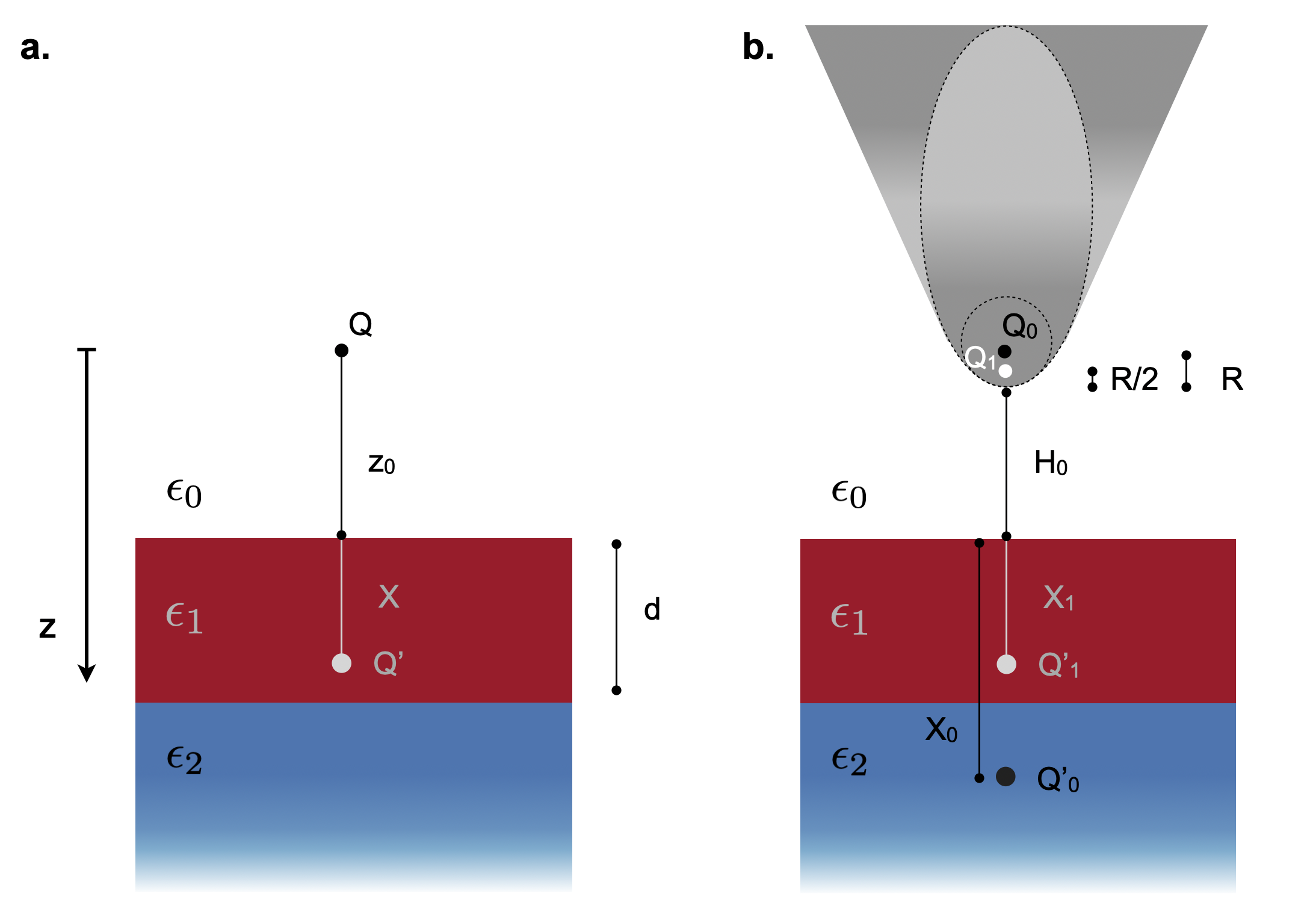
Optical properties of the sample are obtained quantitatively using a detailed model of the tip-sample interaction for the optimal interpretation of the experimental data. In our work we make use of the so-called finite dipole model (FDM) to describe the sSNOM response. In particular we have extended upon existing formalisms [19, 20, 21] to model our system which comprises of up to seven layers. Moreover we developed an analytical formalism which deals with complex valued dielectric functions.
Within the FDM the tip is approximated as a prolate spheroid with major axis length and radius at the tip apex. The measured scattered field, containing the optical properties of the sample underneath the tip, is proportional to the polarisation of the tip resulting from the incident external illumination and the near-field interaction with the sample. Within the FDM the effective polarizability of the tip reads as [19]:
| (S1) |
where and are functions specific to the geometry of the problem:
| (S2) |
Here is an empirical geometrical factor, which describes the portion of the near-field induced charge in the tip, relevant for the interaction. For typical sSNOM tip geometries, . are the positions of the charges in the sample imaging the charges and in the sample, as shown in Fig. S2b.
2.1 Extension to multi-layered samples
The extension to the multi-layer case has been obtained [20] through the analytical solution of the boundary value problem for the electrostatic potential in ferroelectric thin films below an AFM tip [32]. In this section we provide an extension of the derivation of the multi-layer finite dipole method (MLFDM) able to describe systems consisting of up to seven layers.
We consider a mutilayered setup as in Fig. S2a. Our aim is to find how the potential above the sample is affected by the layers underneath. The potentials in the different layers are given by [32]
| (S3) | ||||
| (S4) | ||||
| (S5) |
The complex-valued coefficients and can be found by solving the boundary conditions of continuity of the potential at the interface for all values of . Thus at the boundary between the and layer, determined by the position , we impose:
| (S6) | |||
| (S7) |
Hence, the system of equations obtained in case of the three-layer system (see Fig. S2a) reads:
| (S8) |
Solving the boundary conditions at all the interfaces in the system, we obtain
| (S9) | ||||
| (S10) | ||||
| (S11) |
In a more compact form, the potential above the sample reads [32]
| (S12) | |||
| (S13) |
Here is the electrostatic reflection coefficient, which represents the key quantity for the knowledge of the optical properties of the material, and it is defined as
| (S14) |
with and being the dielectric functions of the two interfacing materials.
We emphasise that the contributions from the layers underneath the tip are implicitly encoded in the function . Therefore, if up to layers are considered, will depend on further terms, which we denote , with .
In the case of multiple layers, can be written in a compact form:
| (S15) |
where is the sum of the thicknesses of all the layers. The functions and changes according to the number of layers considered. Below we provide their analytical form up to 7 layers.
- •
MLFDM with four layers:
(S16) (S17) - •
MLFDM with five layers:
(S18) (S19) - •
MLFDM with six layers:
(S20) (S21) - •
MLFDM with seven layers:
(S22) (S23)
In our calculations we use the multi-layer model to describe the different stacks in the sample. In particular, we use a 3-layer model to describe the stack Air/Bi2Se3/SiO2, a 4-layer model for Air/Bi2Se3/Air/SiO2 and a 5-layer model for Air/Bi2Se3/Air/Au/SiO2. Moreover, a higher number of layers allows a more detailed characterisation of the TINR split up into 3 layers: a middle bulk layer, and two thinner top and bottom surface layers for an approximate model of the TI surface states.
In the FDM formalism, the potential response above the sample is approximated by the potential of a point charge at a distance under the sample surface. In particular
| (S24) |
where is the distance from along the z direction as shown in Fig. S2a. To determine the values of and we impose that, at , the potential (in Eq. S24) and electric field component in the direction coincide with the response (in Eq. S12). Thus
| (S25) |
Therefore:
| (S26) |
Notice that, different from Eq.(9)-(10) in Ref. [20], it is crucial to consider the absolute value of the potential to assure that is defined as a real number. The phase is then encoded in the effective quasi-static reflection coefficient .
2.2 Analysis

In Fig. S3 we show the theoretical prediction for the near-field signal for different thicknesses of the Bi2Se3. It can be seen that as decreases, the signal of the Bi2Se3 converges to the SiO2 response, while for nm, the Bi2Se3 signal converges to the response of bulk Bi2Se3, meaning that the nanoribbon screens almost completely the effect of the SiO2 substrate. This analysis emphasises that a multi-layer model is necessary to predict the optical responses of a system characterised by thin layers. This is further confirmed if comparing the computed signal in Fig. S3a and the measurements in Fig. 3a-b of the main manuscript, where it can be noticed that a bulk model for Bi2Se3 does not provide good agreement with the measured near-field values. Moreover, the observation of the SiO2 fingerprints in sSNOM measurements atop the Bi2Se3 nanoribbon shows that the thickness of the Bi2Se3 is appropriate to classify it as a thin layer.
In Fig. S3b we study the behaviour of the effective position computed using Eq. S26. We observe that shows frequency-dependent features for a multi-layered sample, while in case of the bulk Bi2Se3 or SiO2, is constant. The latter behaviour can be further confirmed considering the convergence of the Eq. S13 to the bulk limit. This is achieved setting and (therefore ). Under this assumption, the potential above the sample becomes:
| (S27) |
Notice that the convergence of the integral above is achieved in the limit of . We then compute the effective position of the image charge and . The results read:
| (S28) |
which corresponds to the expected values for a sample with a single layer, where in Fig. S2 is defined as () when considering ().
In Fig. S3c we outline the behaviour of the quasi-static electric coefficient relative to the point charge at a position below the sample surface. We remind that the this is a key quantity as it encodes the optical responses of the multi-layered sample. Its behaviour resembles the one of the near-field signal (see Fig. S3a). The quenching of the peak at cm-1 outlines that the screening of the SiO2 increases when a thicker layer of Bi2Se3 is considered.
These observations emphasise the important role of the multi-layer model in providing a quantitative description of the sSNOM measurements.
3 From Model to Measurements
In this section we outline how we fit the model to the measured approach curves. We start by describing the obtained measurements and their post-processing. This initial step is then followed by the calibration of tip parameters through the fit of the measurements with the theoretical predictions.
3.1 Analysis of the raw data
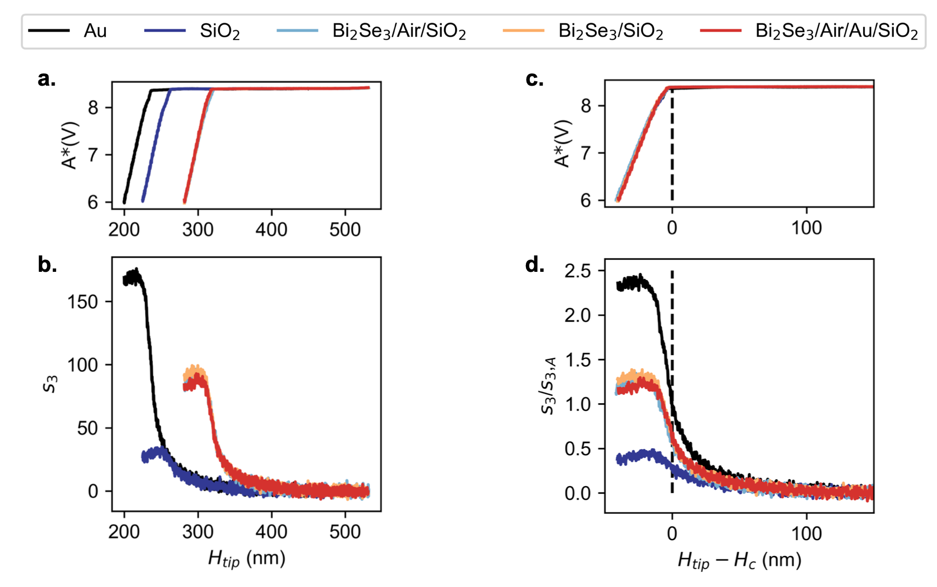
The approach curves shown in Fig. S4b outline the behaviour of the near field signal in function of the tip position. Notice that the tip is in tapping mode, with an oscillation frequency of kHz, 9 orders of magnitude slower than the IR frequency,hence it can be regarded as stationary at any instant, with equilibrium position . The raw data, shown in Fig. S4b, do not report explicitly the information of the tip-sample distance , but rather the near-field signal is recorded as function of the tip’s absolute height . As a consequence, the approach curves measured at different positions of the sample do not have an aligned zero height value. To proceed with the modelling, we need to extract the reference distance of the tip in contact with the sample. To this aim we use the recorded oscillation amplitude .
The raw data for the tip oscillation amplitude shown in Fig. S4a is the photodetector response (in volts) as a red laser illuminates the back of the oscillating cantilever, as in a conventional AFM. The measured represents the first harmonic of the oscillating laser intensity.
From Fig. S4a we can see that the tip is oscillating at a constant amplitude up to a critical height, below which it starts to decrease. We associate the inflexion point of to the reference position, where tip gets in contact with the sample at the point of maximal extension during the oscillations. We set this point as the boundary between non-contact and contact tapping mode. In the contact tapping mode, the motion of the tip is distorted for part of the oscillation and the measured oscillation amplitude decreases. Note that for heights only slightly below this point the distortion of the oscillation from a pure sinusoidal is small. The details of the modelling of this behaviour are reported in the next section, where we discuss how to calibrate the tip parameters. In particular, to convert the data in volts to actual oscillation amplitudes in nanometers, the scaling factor is obtained via the fitting procedure discussed in the next section.
Once the reference height described above is obtained for each curve, the curves in the data set can be shifted along the x-axis, resulting in all being aligned with respect to the tip sample distance , see Fig. S4c-d.
The next step of the post-processing involves the shift of the data along the y-axis by removing the background signal, which is represented by the non-zero near-field value observed in the approach curves at long distances from the sample. Analysing the measurements performed on the system of interest, we note that the background signal is more relevant for low harmonics () than higher harmonics () which are instead less affected by far-field effects. We determine the value of the background signal averaging the data at the tail of the signal, in a range between 120 and 150 nm height from the sample (Fig. S4c-d). Hence, it is important that the measurements are performed up to sufficiently large tip-sample separation to fully capture far-field effects. At last, the signals must be re-scaled with respect to a known reference signal, which in our case is represented by the signal of Au at . We point out that the procedure shown in Fig. S4 is for a fixed IR frequency cm-1. The vertical shift of the background signal and the re-scaling with respect to the reference material (Au) need to be repeated for all the different frequencies in the data set.
3.2 Tip Parameters Calibration


The effective polarizability of the tip, introduced in Eq. S1, depends on the geometry of the tip and on the optical properties of the sample considered. The unknown geometrical parameters are obtained through the fitting of the approach curves of a reference material whose optical response is well known. In our case we consider the near-field signal obtained atop Au.
Fitting procedure of the tip geometrical properties.
The FDM curves are obtained from the Fourier transform of Eq. S1, with the dielectric function of Au for a fixed wave-number and a set of initial guesses for . The tip-sample distance and the oscillation amplitude are the measured quantities, as shown in Fig. S4. The time varying position of the tip is described in our model by the equation
| (S29) |
where is the oscillation amplitude re-scaled from Volts to nanometers. Consistently to what is performed in the post-processing of the measured data, the near-field values obtained with the FDM model are shifted by the background signal. Secondly, the obtained theoretical approach curves for Au in Fig. S5a are of a different order of magnitude with respect to the measurements shown in Fig. S4b. To properly match the theoretical with the experimental curve, a multiplicative factor is obtained considering the ratio of the two curves. We emphasise that this multiplicative factor is important only for getting the geometrical properties of the tip and does not play any role when re-scaling the full data set with respect to the Au reference. Furthermore, the ratio should not depend on the different near-field harmonics. Therefore in our procedure we compute from the ratio of the computed and measured second harmonics of the signal. Then, to validate this fit we re-scale the computed values for and compare them with the measurements.
In Fig. S6 we report the comparison between the measurements and the theoretical curves obtained via the FDM method, using different combinations of values of tip radius , tip length , -factor, and oscillation amplitude . Our study reveals that the optimal parameters are: nm, , nm for the particular tip used in these experiments.
Tapping modes and time dependent model for the oscillating tip.

The validity of the finite dipole method holds in the case of smooth sinusoidal behaviour of the oscillating tip. When the tip gets in contact with the sample, its motion is distorted and the measurements reveal a consequent drop of the oscillation amplitude. Therefore, for a consistent quantitative benchmark between the theory and the measurements, we need to distinguish the limits of the different regimes. As shown in Fig. S4, we can detect the boundary between the contact and non-contact regime from the analysis of the behaviour of the measured tip oscillation amplitude. In this section we analyse the validity of the model for different selection of the height at which we determine that the tip is in contact with the sample. The FDM curves are obtained from Eq. S1, with fixed tip parameters as described above and cm-1. For a better description of both tapping mode regions, we extend our model for the tip as follows:
| (S30) |
where the oscillation amplitude and the distance are simultaneously measured.
In Fig. S7 we show the behaviour of the oscillation amplitude and we characterise the different tapping modes. As previously stated, the inflection point establishes the distance at which the tip is in ’contact’ with the sample and the boundary between what we here in the context of sSNOM label as the contact and non contact regime. A closer analysis at the contact mode region, reveals that the approach curves show the same trend as in the non contact mode, until a plateau is reached. This observation allows us to distinguish two different regimes of the contact mode, which we here label as soft and hard tapping regimes.
We found that the FDM model provides an exact description of the measurements performed in a non contact regime, it shows a fair agreement if the truncation of the data is performed in the soft contact mode, while it fails in the hard tapping regime. Furthermore the extended Eq. S30 captures the observed plateau trend, albeit at incorrect values which is to be expected as Eq. S30 only provides a simplified picture of damped tip oscillations, and disregards any non-linearities due forces acting on the tip. The exact description of tip dynamics able to describe the two contact regimes is left for future research. When analysing approach curves we instead focus on the data in the non contact regime.
3.3 Dielectric Functions
In this section we outline the dielectric functions used to model the different materials present in the experiment.

| (cm-1) | (cm-1) | ||
|---|---|---|---|
| 1 | 1122.27 | 67.2179 | 0.6752 |
| 2 | 805.20 | 75.7996 | 0.0929 |
| 3 | 457.61 | 44.5774 | 1.0218 |
SiO2 substrate
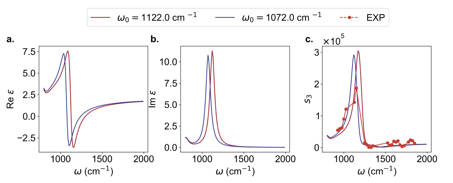
We assume the SiO2 to be the bottom-most ’bulk’ layer in the FDM as its thickness (300 nm) is large enough such that anything underneath no longer contributes to the near-field response. This assumption is well justified given the much smaller tip radius and the fact that the different thicknesses of SiO2 on the sample (due to the trenched regions) produces no measurable difference in the sSNOM response. The SiO2 substrate is modelled in the spectral region of interest as a Lorentz oscillator:
| (S31) |
whose parameters are defined in Tab. S1 and .
Gold regions
The Au regions were modelled with a Drude model with fs and eV [22].
Bi2Se3 nanoribbons
The Bi2Se3 nanoribbon was simulated with a Drude model, which reads
| (S32) |
where and scattering rate cm-1. with effective mass where is the free electron mass [23]. In our study the carrier concentration values which better describe the system are in a range cm-3.
Our parameters are similar to the ones used in Ref. [13] where the Bi2Se3 nano-crystals were modelled with a scattering rate cm-1, , and cm-3. A better agreement with measurements is achieved in our case with cm-1. A lower scattering rate is indicative of the presence of less impurities and therefore higher quality of the synthesis. Furthermore, in Ref [34] where optical properties of thin films were studied, the following parameters were found: cm-1, and cm-1. The small damping parameter of the dielectric function is due to less defects arising from the epitaxial growth of the thin film.

| (cm-1) | (cm-1) | ||
|---|---|---|---|
| 1 | 1650 | 40 | 20 |
| 2 | 1800 | 50 | 20 |
As discussed in the main text, the experimental data show additional peaks at cm-1 and cm-1. These peaks can be included in our MLFDM calculations (see Fig. S10) by assuming a multilayer description of the Bi2Se3 nanoribbon. We define an additional thin surface layer (of 5 nm) on top of the thick bulk layer (on 80 nm). In particular, the dielectric responses of the two layers of the TINR are modelled with a bare Drude model (Eq. S32) for the bulk layer and two additional Lorentz terms (Eq. S32, Tab.S2) for the thinner layer which captures the measured response well. We note that introducing this additional layer on the bottom of the TINR yields an identical response, except for a lower amplitude, meaning we are unable using the model to determine which, if not both, surfaces this response originates from.
4 Frequency spectra
In this section, we extend the analysis of the frequency-dependent spectra of the near-field signal shown in Fig. 3 in the main text. In particular, we provide further details on the post-processing required to obtain the frequency spectra from the two sets of measurements in analysis (approach curves and 2D scans), and the modelling of the carrier concentration of the Bi2Se3 nanoribbon atop different substrates.


Spectra from approach curves.
The frequency-dependent values of the near-field signal can be extracted from the post-processing of the approach curves. As already outlined in section 3, the approach curves are recorded with the tip fixed atop different sample locations and by varying its distance from the sample. The locations are chosen such as to have sufficient separation between regions in order to avoid finite-size effects. In Fig. S11 we report the near-field values extracted at a fixed distance of the tip for different frequency values. Notice that the three columns represent the measurement extracted at the three different tapping regimes (hard, soft and non contact mode) as indicated in Fig. 2b of the main text.
The major response is measured when the Bi2Se3 nanoribbon is on top of Au, and the relative position of the yellow and blue line emphasises the different response of the Bi2Se3 when it is suspended or in contact with the SiO2 substrate, and we consistently observe a difference in the range 1200-1600 cm-1. Inconsistent features across the three panels are observed only between 1000-1200 cm-1. In this frequency range the sSNOM signal is generally very weak which results in increased noise and uncertainty.
Spectra from surface scans.
In contrast to approach curves, the measurements extracted from the 2D surface scans are for a fixed distance of the tip from the sample, and scans cannot be taken in what we here define as the non contact sSNOM regime where the FDM model is valid. For all scans we use an AFM amplitude set-point of % of the free oscillation amplitude, which is within the soft tapping regime.
To validate the observation that the optical response of the Bi2Se3 nanorribbon differs whether suspended or in contact with the SiO2 substrate, we take into consideration measurements of the Bi2Se3/SiO2 performed on different positions along the Bi2Se3, as shown in Fig. S12a, chosen such as to have maximal separation and avoiding significant contributions due to any finite-size effects (here relevant for length-scales nm). Again we observe in Fig. S12b that the signal measured on the stack Bi2Se3/SiO2 is larger than the signal measured in presence of the air gap (Bi2Se3/Air/SiO2), for all the different areas analysed.
In Fig. S12c some weak signatures of the two peaks at 1600 and 1800 cm-1 can be seen even when the tip is atop SiO2 alone, due to far-field coupling of the lower harmonics. However, for higher harmonics in Fig. S12d these peaks disappear, indicating that for higher harmonics finite-size effects are irrelevant on length-scales m, the distance away from the Bi2Se3 that the bare SiO2 was analysed. This also confirms that the two additional peaks at 1600 and 1800 cm-1 indeed originate from the Bi2Se3 itself.
MLFDM results.
In Fig. S13 we report the results obtained for different Bi2Se3 carrier concentrations. The theoretical model allowed us to establish a finite range of possible carrier concentrations which properly fit the frequency dependent behaviour. The comparison of the different panels reveal that the system analysed is correctly described only if the carrier concentration is in the range cm-3.