The Majorana Demonstrator Readout Electronics System
Abstract
The Majorana Demonstrator comprises two arrays of high-purity germanium detectors constructed to search for neutrinoless double-beta decay in 76Ge and other physics beyond the Standard Model. Its readout electronics were designed to have low electronic noise, and radioactive backgrounds were minimized by using low-mass components and low-radioactivity materials near the detectors. This paper provides a description of all components of the Majorana Demonstrator readout electronics, spanning the front-end electronics and internal cabling, back-end electronics, digitizer, and power supplies, along with the grounding scheme. The spectroscopic performance achieved with these readout electronics is also demonstrated.
1 Introduction
The Majorana Demonstrator’s [1] searches for neutrinoless double-beta decay [2, 3, 4] and other physics beyond the Standard Model place stringent requirements on the design of its readout electronics. The need to separate neutrinoless double-beta decay signal events at 2.039 MeV (the Q-value of 76Ge double-beta decay) from the two neutrino double-beta decay events (a continuum with energy up to the Q-value) necessitates excellent energy resolution, and therefore low-noise readout electronics. To realize a sensitive search, backgrounds induced by cosmic rays and other natural radioactivity are minimized by locating the experiment underground at the 4850-ft level of the Sanford Underground Research Facility (SURF) [5] in Lead, SD, USA, and by judicious selection of detector construction materials [6]. These features also enable sensitive searches for physics beyond the Standard Model at low energies ( keV) [7, 8].
The Majorana Demonstrator (Figure 1) comprises two independent modules, each containing a vacuum cryostat with its own separate vacuum and cryogenic systems. Inside each cryostat, seven strings holding up to five p-type high-purity germanium (HPGe) detectors each are suspended from the copper cold plate, a large conductive thermal mass to conduct heat away from the detectors. The cryostats are surrounded by copper and lead shielding, enclosed in a radon exclusion box. Both the inner shield and the copper parts inside the cryostats are made out of electroformed copper produced and machined in the Majorana Demonstrator’s underground laboratory [9, 10]. The active muon veto system [11, 1], which comprises plastic scintillator panels, locates outside the radon enclosure. Each cryostat is connected through the shielding to its vacuum and cryogenic systems and its warm electronics via the crossarm. Two custom vacuum feedthrough flanges are located at the end of each crossarm. Mounted directly on each flange are the electronics boxes that contain the back-end electronics. Polyethylene shielding (“poly shield”) surrounds all of this apparatus. The digitizers and power supplies are located in equipment racks outside the poly shield.

Each of the two modules consists of both 76Ge-enriched p-type point-contact (PPC) detectors [12, 13] and commercial Broad Energy Germanium (BEGe) detectors [14]. The bulk semiconducting material of the PPC detectors is p-type. The small single “point” contact for charge collection in a PPC detector results in a small capacitance of 2 pF. Each detector’s bias voltage is applied on the n+ contact. The p+ contact is electrically connected to a low-mass front-end (LMFE) board [15] for signal charge amplification. The internal cabling routes from the detectors to the cold plate, then through the crossarm to the feedthrough flanges and the electronics boxes. The mapping of detectors to the power supplies and components of the readout electronics is designed to be flexible. In the configuration implemented in the Majorana Demonstrator, the detectors of a string share a common high-voltage power-supply module. Individual channels of the module can supply each detector with a different operation voltage (HV, 0 to 5000 V). Each custom-built low-voltage (LV, -24 to 24 V) power supply powers the motherboards, preamplifier cards, front-ends, and a controller card for two strings of detectors. The differential output signals from the preamplifier cards are sent to digitizer cards.
From May to October 2015, only Module 1 was instrumented. It contained twenty 76Ge-enriched PPC detectors with a total mass of 16.8 kg along with nine natural BEGe detectors with a total mass of 5.6 kg. Module 2 was deployed in mid-2016 with fifteen 76Ge-enriched PPC detectors with a total mass of 12.9 kg and fourteen natural BEGe detectors with a total mass of 8.8 kg.
The default electronics configuration is shown in Figure 2. The order of presentation of this paper follows the path of the charges collected from the detectors, approximately from right to left in the figure. In Sections 2 and 3, we describe the front-end electronics and the internal cabling inside the vacuum cryostats. Section 4 presents the back-end electronics outside the vacuum. In Section 5, we describe the signal digitizer card along with the high-voltage and low-voltage power supplies. In Section 6, we review the grounding scheme of the experiment. The spectroscopic performance of the Majorana Demonstrator is shown last in Section 7.

2 Front-end electronics
The low-mass front-end [15] board is the first element in the detector signal amplification chain. They are mounted in close proximity ( cm) to each detector’s point contact to minimize noise. To enable their placement so close to the detectors, radioactive backgrounds in the LMFE were minimized through its low-mass design and careful selection of components [6].
The LMFE (Figure 3) is built upon a rectangular 20 mm x 7 mm substrate of 200 m thick fused silica (Corning® 7980). On each LMFE is a bare-die Moxtek MX-11 [16] junction gate field-effect transistor (JFET) whose properties are shown in Table 1, a feedback resistor ( G), and a feedback capacitor (0.17 pF) in a resistive-feedback configuration. The feedback capacitance is provided by the capacitance between traces, as is the 45 fF capacitance used for injecting pulser signals (discussed in Section 4.3) to the gate of the JFET. The traces are sputtered 20/400 nm Ti/Au, and the drain and source of the JFET are wire-bonded to the traces with 25.4 m Al(1% Si) wires. The gate on the bottom of the JFET is affixed to its trace on the fused silica with low-outgassing silver epoxy (Henkel Hysol® TRA-DUCT 2902). This epoxy is stable under temperature cycling and has demonstrated acceptable radiopurity under assays.
| Property | Measurement Conditions | Value |
|---|---|---|
| Leakage Current | Single Junction, T C | pA |
| Transconductance (gm) | V V, I mA, T C | 5.6 mS |
| V V, I mA, T C | 4.1 mS | |
| Cut-off Voltage (Voff) | V V, I nA | –4.2 V |
| Drain Saturation Current (IDSS) | V V, V V | 30 mA |
| Gate-to-Source Capacitance (CGS) | V V, I mA, 1 MHz | 2.70 pF |

Each LMFE is mounted in a custom-designed spring clip, machined in an underground cleanroom out of electroformed copper. The circular pad end of the LMFE is inserted into a slot in the clip, and the other end is fixed onto the clip with Henkel Hysol 0151 epoxy. Photographs of the LMFE in a spring clip and the surrounding detector-mount components are shown in Figure 4. The electrical connection between the LMFE readout pad and the detector’s charge-collecting electrode is made by a contact pin cm long and cm in diameter. The pin is made out of electroformed copper and coated at both ends with high-purity tin provided by Canberra (now Mirion Technologies (Canberra) Inc [14]). The spring-clip aligns the LMFE pad with the contact pin, which is held in place by a polytetrafluoroethylene (PTFE) bushing. Three #4-40 electroformed copper nuts, which have been coated with parylene as a lubricant to prevent galling, are used to secure the spring clip to the detector mount. The end of the spring clip with the cable connections is attached to the detector mount with two of these nuts, while the other end is fastened to a threaded stud with one nut. Turning this nut controls the tension on the contact pin. In the Majorana Demonstator, this nut is tightened to provide just under 7 N of force between the LMFE and the contact pin, which ensures good electrical contact and reduces microphonic noise without damaging the fused silica substrate.


The feedback resistor is a 400-nm-thick film of sputtered amorphous germanium, which has low 1/f noise and radioactive background. The resistance of the film varies with temperature T (in Kelvin) as exp(T) (Figure 5), requiring a stable operating temperature. Any resulting variances in the preamplifier decay times between detector channels can be monitored with in-situ pulsing and are readily addressed during pulse shape analysis of the digitized pulse data [3].
The resistor geometry was designed by considering the heat dissipation of the JFET and the resulting temperature gradient on the LMFE to achieve the desired resistance (Figure 6). The drain-source voltage (VDS) is user-adjustable between 0 V and 4.1 V through the controller card to compensate for temperature variances. This adjustment can be made via the ORCA (“Object-oriented Real-time Control and Acquisition”) system [18]. A nominal value of V is set to produce a -mA drain current (), resulting in the JFET dissipating mW as heat. The temperatures of components on the LMFE depend on the temperature of the copper clip, which is estimated to be at approximately 85 K (as opposed to the liquid nitrogen temperature of 77 K) due to its mounting position in the detector string and heat loss in the detector system. The operating temperature of the JFET is about K, where near-optimal noise performance is achieved. The temperature gradient along the resistor results in its effective temperature at K, leading to the G resistance that optimizes noise performance. This gives a decay time constant of 1.7 ms at the output of the first stage of preamplification. Combined with the capacitive coupling to the second stage of amplification (required since the first-stage baseline was outside the dynamic range of the digitizer), this results in a decay time constant of s for the digitized signal. This is suitable for both the normal detector event rate ( Hz) and the higher event rate during calibration ( Hz) [19].

The LMFE has four traces for connections to an external pulser, JFET drain, JFET source, and the feedback capacitance and resistor in parallel. These traces are each connected to the central conductor of an Axon’ pico-coax cable with the same silver epoxy used to attach the JFET gate. The cables are woven through three rows of holes for strain relief. These holes were ultrasonically drilled in the substrate by Bullen [20].
Figure 7 shows the typical noise curves measured using an LMFE-based readout under different conditions. All detectors had low capacitance, approximately 2-3 pF. As a result, the series noise was very low. A prototype LMFE operated without the additional capacitive load of a detector achieved a minimum noise level of 55 eV FWHM (full-width at half-maximum). When mounted on a small prototype PPC detector with a small p+ contact (the “mini-PPC” [15]), a minimum noise of 85 eV FWHM was achieved. When mounted in a test string of three detectors (one Majorana PPC and two BEGe detectors) using the full Majorana production electronics, a minimum noise level of 221 eV FWHM was achieved with a integration time of 5.9 s.
3 Internal cabling
The internal cabling consists of two different coaxial cable designs. The signal cables connect the pulser, drain, source, and feedback traces on each LMFE to the preamplifier card. The HV cables deliver the bias voltage to the detectors. The internal cabling for each module routes through two CF8 feedthrough flanges located outside the lead shielding, as shown in Figure 1. Each feedthrough flange has four 50-pin D-Sub connectors (DD-50). Each connector can connect to six detectors (a pin for each of the four signal cables and their ground shields, for a total of 48 pins). Each flange also has 40 “Pee-Wee” connectors (SRIPW101 from SRI Hermetics), rated to 12 kV DC, for the bias high voltage and returning ground for up to 20 detectors. The feedthrough flange is shown in Figure 8.


3.1 Internal signal cabling
Internal signal cables were custom produced by Axon’ Cable in Montmirail, France, using materials pre-screened for radiopurity. Based on the Axon’ PicoCoax® design, the internal signal cables consist of a 0.076-mm diameter central conductor provided by California Fine Wire, an uncolored 0.254-mm outer diameter fluorinated ethylene propylene (FEP) dielectric, strands of 0.02504-mm diameter copper wires forming a helical shield, and a 0.4-mm outer diameter FEP jacket. The resulting cables have a characteristic impedance of 55-58 and a capacitance of 87 pF/m, depending on the production batch. The linear mass density is 0.4 g/m.
The total length of signal cable between each LMFE and the feedthrough flange is 2.15 m. This is broken up into two runs: one between the LMFE and the cold plate, and the other between the cold plate and the flange. Four coaxial cables in a bundle are used for each LMFE, for each of the two runs. On the vacuum side of the flange, the signal cables are soldered to D-Sub sockets using low-radioactivity solder (one for the central conductor, and one for the shield), which are then inserted to the D-Sub receptacles on the flange.
Above the cold plate, custom connectors [21] are needed to meet Majorana Demonstrator’s background specifications. Electrical contact springs in commercially available connectors typically contain beryllium-copper (BeCu), which has unacceptably high radioactivity. Contact force is necessary to maintain a robust connection under temperature cycling. A spring-free design is used, using commercial Mill-Max gold-plated brass pins (8210 Receptacle with a Standard Tail) produced in a special run without BeCu spring inserts, housed in a Vespel body custom-machined in the Majorana Demonstrator’s underground machine shop. The pins and sockets are slightly misaligned radially, so that the contact force is provided by the forced bending of the pin as it is inserted into the socket. A low-background tin-silver eutectic developed for the SNO experiment [22] is used to solder the cables to the connector pins and sockets. FEP shrink-tubing provides strain relief for these connections (Figure 9).


High-precision machining is required for fabricating these custom connectors to maintain a secure connection. But electrical discontinuity was observed during thermal cycling in a subset of these connectors. Additionally, some connections in successfully bench-tested D-sub commercial connectors failed in the field, reducing the number of available spare channels. Possible explanations for these failures include mishandling at installation, inadequate strain relief, and deflection of the connector body that prevents robust contact in the central region of the connector. In at least one instance, electrical shorts have been observed between the signal cable ground shields and the cold plate, implying damage to the signal cables during installation or handling. An upgrade that improves cable routing and connector design completed in early 2020. These improvements will be reported in a future publication on post-upgrade performance of the Majorana Demonstrator.
3.2 Internal high-voltage cabling
The internal high-voltage cables also use the Axon’ PicoCoax® design, but with thicker dielectric to support high-voltage operation. They consist of a 0.153-mm-diameter copper central conductor, a 0.311-mm-thick FEP inner dielectric (0.77-mm outer diameter), a copper helical shield as ground (0.82-mm outer diameter), and a 0.19-mm-thick outer jacket (1.2-mm outer diameter). The resulting cable is rated to 5 kV DC, and has an approximate linear mass density of 3 g/m.
At the vacuum side of the feedthrough flange, each central conductor and ground terminate in commercial BeCu D-sub sockets, housed within a custom-machined 2-pin polyetheretherketone (PEEK) body. The resulting plug is push-connected to the corresponding HV and ground pins on the feedthrough flange.
The connection between the HV cable and a detector’s HV contact ring occurs through contact with a spade-lug connector (the “HV fork”), custom-machined out of electroformed copper. Close to this connector, the outer jacket and shielding of the HV cable is stripped back and protected by FEP shrink tubing to ensure no contact with ground. At the connector, the bare central conductor of the HV cable is woven through two holes, and fixed in the second hole with a Vespel plug.

The high-voltage cables, connectors, and feedthroughs were tested to ensure that micro-discharges would not be induced by the detector bias voltages [23]. All HV cables were tested prior to installation. Nonetheless, the high-voltage cables and connectors also have operational issues.
The most prevalent were the HV breakdowns observed as significant discharges in the cables during their initial operations. To prevent damages to the electronics, these detectors were fully or partially biased down while the cause of the breakdowns was investigated. Once it was determined that the breakdowns were occurring between the HV cable central conductor and ground shield, 11 detectors were brought online by not connecting the shield to ground. Additional tests on spare cables revealed excessive compression during installation as the likely cause of the deformation to produce this problem. Improvements in cable routing and the designs of in-vacuum HV connectors were realized in the upgrade.
4 Back-end electronics
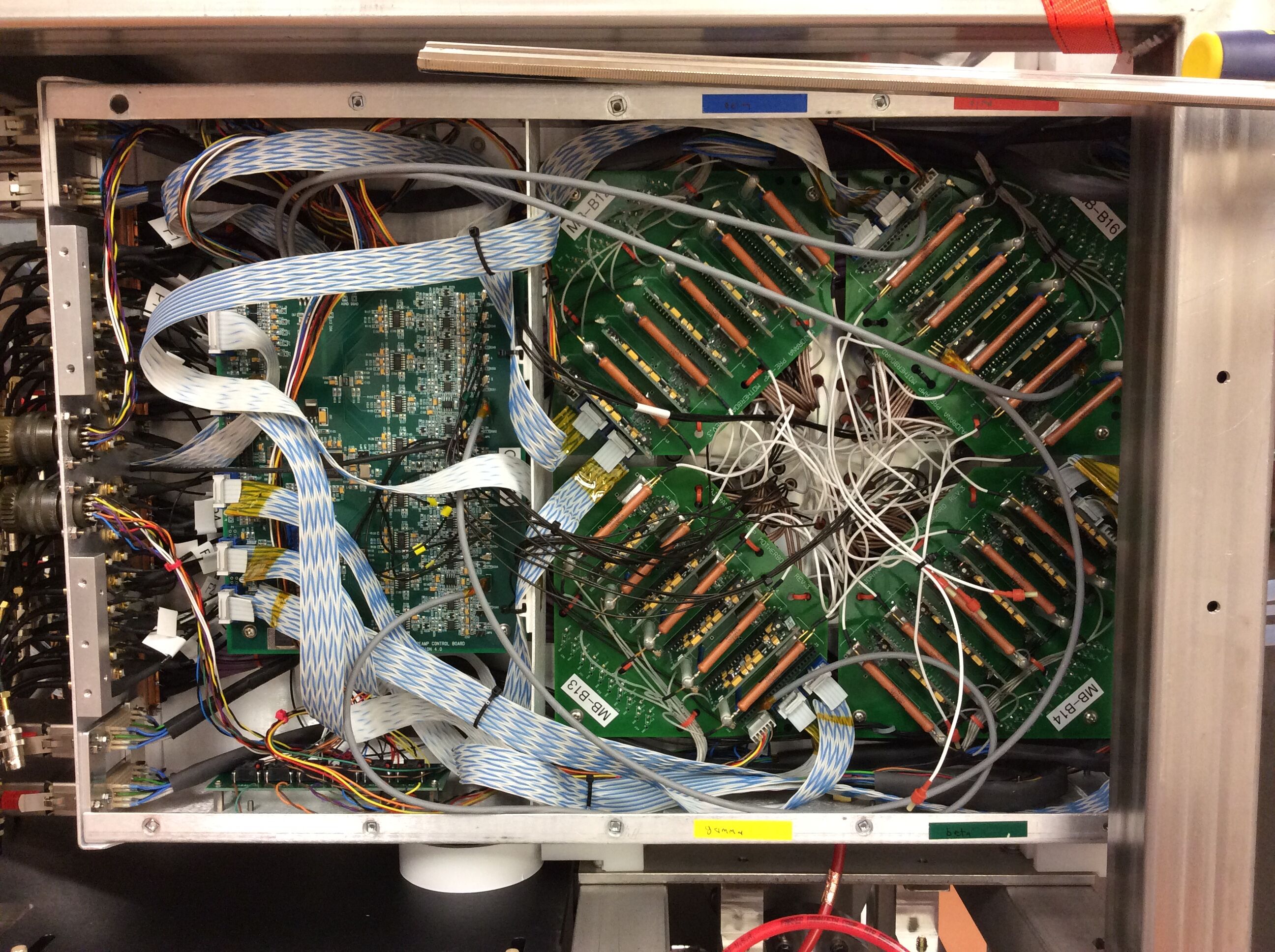
The back-end electronics consist of motherboards, preamplifier cards, and controller cards. These are contained in electronics boxes mounted on feedthrough flanges (two electronics boxes per detector module). Each electronics box contains two controller cards, and four motherboards that fit together with space to access the connections on the air side of the feedthrough flange (Figure 11). A total of 40 W of heat is produced in a fully loaded electronics box. The electronics boxes are housed within the poly shield, whose enclosed volume is actively cooled with a chilled water radiator and a flow of boil-off nitrogen gas.
4.1 Motherboard
Each string of detectors is served by one motherboard (Figure 12). The motherboard has connections for up to five preamplifiers, where the gain loop including the LMFE is closed. The preamplifier outputs are forwarded to the digitizer card. The mapping of strings to motherboards was chosen to utilize working connectors and allow for an equal distribution of spare channels throughout the electronics box.
The output of the high-voltage power supplies is also routed through the motherboard, which contains five high-voltage RC filters, each consisting of a Caddock MG735 1-G 1% resistor and a custom Novacap 8.2nF 7000V capacitor. The HV filters also have a 1-G 5% bleeder resistor (Ohmite MOX1125J-1000ME-ND) to ground for safety. For testing and calibration, charges can be injected into the detector by bypassing the HV filter via a voltage divider.
The low-voltage power supply outputs also route through the motherboard, which distributes power to the preamplifiers and controller cards. The power provided to the JFET on each LMFE is set by the controller cards, and routed to them through the preamplifiers via the motherboard (Section 4.3).
The motherboard is a 4-layer board, utilizing separate ground planes for the preamplifiers and the high-voltage filters. Communication between the controller card and the digitizer is also routed through the motherboard.

4.2 Preamplifier card
To reduce the number of active components (hence background radioactivity) near the detectors, the gain loop for detector signal amplification is spatially separated (Figure 13) between the warm preamplifier card on a motherboard outside the detector shield and the cold LMFE board (Section 2). Together they form a charge-sensitive preamplifier.

The preamplifier uses a folded-cascode design based on the Goulding amplifier [24]. It differs from the Goulding amplifier in its choice of power supply lines ( V and V DC) and in its implementation of a capacitively coupled second amplification stage using operational amplifiers. The output of the first amplification stage is available for diagnostic purposes (e.g. measuring detector leakage current and signal rise-times), and is read out by an ADC in the controller card (Section 4.3).
The second amplification stage provides differential outputs for two separate gains. The dynamic range is to MeV for the high-gain output, and to MeV for the low-gain output. No pole-zero correction is performed by the preamplifier, opting instead for post-processing of the digitized pulse.
During commissioning, pulses were applied to each front-end’s pulser line, and a 1-20 pF trimmer capacitor on each preamplifier was adjusted to remove ringing in the output waveform.
With careful choice of front-end components and a short cable connection, the preamplifier is capable of a sub-10-ns rise time. With the LMFEs and full-length cables used in the Majorana Demonstrator, and the adjustable capacitor on the preamplifier card tuned to prevent ringing, rise times of 120-200 ns were observed at the output of the first stage of the preamplifier card during testing.
4.3 Controller card
The controller cards house the pulser system electronics, as well as circuitries for controlling and monitoring the readout electronics. Each controller card performs these functions for two strings of detectors.
Each controller card contains one Xilinx XC3S200A-4VQG100C Field Programmable Gate Array (FPGA), which is the interface between the optically-coupled SPI bus to the digitizer and the data conversion chips on the controller card. All settings and measurements communicated between the digitizer and controller cards are available in the ORCA slow-control system.
Two Analog Devices AD7327BRUZ analog-to-digital converter (ADCs) provide 16 analog inputs. Four inputs monitor the preamplifier supply voltages, and two inputs are used to monitor the on-chip temperature. The remaining ten inputs monitor the first-stage output of the preamplifiers.
The controller card also contains two Linear Technology LTC2600CGN 16-bit digital-to-analog converter (DAC) chips, whose outputs set the drain-to-source voltage (VDS) of the JFET on each of the front-end boards individually. Adjusting VDS fine-tunes the JFET performance by varying its power.
Each controller card contains two pulse generator systems, each including one LTC2600CGN DAC, four Analog Devices AD8182AR 10-ns switching multiplexers, and eight operational-amplifier-based attenuators, providing a combined total of 16 pulse-generator outputs. These pulse generators are collectively referred to as the pulser system. The amplitude, high/low time, number of pulses, and attenuation are user-specified in the ORCA interface. During normal operation, the pulser period set on each controller card is typically s. Pulser events are used primarily for livetime monitoring, to confirm detector operation in the absence of physics events (due to the low event rate in each detector). They are also used to monitor gain stability and trigger efficiency, and have been used for the validation of digitizer linearity [25].
5 Digitizer and power supplies
5.1 Digitizer
The amplified differential signal is digitized by the GRETINA [26] digitizer card. The card has 10 differential input ports; thus, one card can serve one string of detectors (five detectors with two gains each). Each card also has an auxiliary digital I/O port, which is used to communicate with a controller card (two strings) over the SPI bus.
Incoming waveforms are digitized at a rate of 100 MSample/s by 14-bit 105-MHz flash ADCs, providing a two’s complement signed integer for each sample. Each card has an on-board pre-ADC leading-edge discriminator (LED) trigger, but the Majorana Demonstrator uses a trapezoidal trigger for practically all data taking. This trigger uses the value of the onboard-calculated trapezoidal filter as a trigger parameter. The time synchronization between all digitizer cards is performed by a ‘trigger card’ hosted in the same VME crate that distributes clock signals to all digitizers. Different onboard features can be set, such as multisampling, pole-zero (PZ) correction, and trapezoidal filtering. Energy is re-calculated during data processing, along with corrections such as PZ and ADC non-linearities [3, 25]. The information produced by the digitizer card for a single event/trigger consists of a timestamp, an uncalibrated energy estimate, and a -sample waveform.
With the exception of a three-month period in 2016, all data taken prior to May 2017 used 10-ns time samples, giving a waveform of s in length. During that period and after May 2017, the data has been taken in multi-sampling mode. In this mode, the first s of the waveform is digitized using 10-ns time samples and the samples after that are 40-ns long, giving such sample waveform a length of s. Multi-sampling retains full detail in the rising edge of the peak needed for multisite-event rejection [27], while allowing digitizing more of the falling part of the waveform to improve alpha-background rejection [28, 29].
5.2 High-voltage power supplies
The high voltage to bias the detectors is provided by ISEG EHS8260p_105 modules hosted in a WIENER MPOD crate. These power supplies have low ripples ( mV), which is needed for good energy resolution and pulse shape analysis performance. The modules can deliver up to kV on 8 channels with return lines isolated (i.e. no common ground). The HV is controlled through customized scripts (e.g. ramp-up, ramp-down) in the ORCA interface. Each detector is limited in ORCA to never exceed its target operating voltage. In no situation can a detector voltage exceed 5 kV even if the voltage target was improperly set. The high-precision readout mode was enabled in the SNMP Ethernet communication with the MPOD controller card to closely monitor the current delivered by the supplies. If this current exceeds an ORCA-preset maximum threshold of 20 A, the HV is shut down to protect the detectors. The safety-loop feature of the EHS8260p_105 modules was also hardware-enabled for integration in the interlock system described in the next section.
5.3 Low-voltage power supplies
A custom-designed low-noise power supply provides power to the controller cards, preamplifier cards, and the JFET on each front-end. The low-voltage power supply module provides six independent voltage outputs from regulated linear supplies, each with isolated returns. Four rails (24 and 12 V) are distributed to the preamplifiers, while the last two (7.5 V) and an unregulated rail (12 V) are used for the controller card. As described in Figure 2, one LV module provides power for two strings of detectors and their associated controller card.
For interlocking with the HV modules, a relay-based logic was implemented to divert a small fraction of current from the unregulated 12 V supply if all of the other supplies provide the expected outputs. This current flows through the safety-loop circuit of the ISEG HV modules that power the same strings of detectors. If the LV is off or turned off, no current flows through this loop and the HV supplies will be biased down to protect the front-end electronics.
6 General grounding scheme
In the Majorana Demonstrator underground laboratory, the “general ground” is a copper stake driven into the floor of the electrical utility room, where the electrical breakers are located. The experiment is in a separate room (“the detector room”). The AC power lines from the electrical breakers to the detector room provide one connection to the general ground. There is also a ground plate mounted low on the wall in the detector room with a dedicated low-resistance ground cable to the general ground.
In the general grounding scheme (Figure 14), electronics components are grouped by their location into three isolated conductive bodies in the detector room: the equipment racks, the exterior of the module (components outside the vacuum), and the interior of the module (the thermosyphon and internal structural copper parts.) The connection between these bodies and ground was carefully planned and executed in order to minimize electronics noise from ground loops.
The three equipment racks are conductive bodies: one for each of the two modules housing the power supplies (HV and LV) and DAQ electronics, and one for slow controls and monitoring. The computers in each rack are powered by the outlets in the iBootBars (Dataprobe iBootBar N15). Each outlet can be remotely controlled for rebooting of equipment and computers. The iBootBars connect to the general ground via the AC power lines. Each equipment rack is grounded via its connection to the iBootBars. The HV and digitizer modules are therefore grounded through their crates to the rack, and the LV power supplies are grounded through their cases to the rack. The returns of the HV modules and LV power supplies are all isolated from the conductive body of the equipment racks, instead of being part of the exterior-of-module conductive body.
The “exterior-of-module” conductive body contains the electronics outside each module, i.e. the electronics boxes (controller cards, motherboards, and preamplifier cards) as well as the wall of each module’s cryostat, and the exterior of the crossarm. These bodies are separated by glass isolators and plastic supports from the surrounding metallic support structures, which have their own paths to ground. The ground planes of the controller cards, motherboards, and preamplifier cards are all grounded to the electronics-box case through metallic standoffs. The power cables from the LV power supplies to the electronics boxes are grounded to the respective box. The cables from the digitizers and the HV power supplies to the electronics box are grounded at both ends, providing the connection of the exterior-of-module conductive body to general ground through the equipment racks.
The “interior-of-module” conductive body consists of the internal structural copper parts (thermosyphon, cold plate, and string assemblies). At each of the module’s two feedthrough flanges, a spare HV cable is plugged into an unused HV channel ground wire and bolted to the cold plate. This grounds the interior-of-module to the exterior-of-module conductive body. A glass isolator between the copper thermosyphon and the rest of the cooling system ensures that these cables are the only ground path for the interior-of-module conductive body.
7 Spectroscopic performance
The spectroscopic performance of the full production readout chain is summarized in this section. In Figure 15, the measured noise (FWHM) and threshold of each detector in a typical physics run are shown. The noise is calculated using the RMS of the signal baseline samples. The threshold is taken from the value loaded into the GRETINA digitizer, corrected for a small offset in the on-board threshold trapezoid value that can change (and is determined independently) after every initialization of the digitizer board. Both are converted to energy values based on a rough energy-scale calibration (which is accurate to within 5%). n The average noise level of eV is crucial in delivering good energy resolution. The sub-keV thresholds enable low-energy searches for physics beyond the Standard Model. The Majorana Demonstrator is the only neutrinoless double-beta decay experiment that triggers at such low energies to engage in such searches.
In Figure 16 the full energy spectrum from a Th-source calibration is shown along with the measured energy resolution as a function of energy. The energy resolution of 0.12% at the Q-value of 2039 keV [2] is the best energy resolution of any operating neutrinoless double-beta decay experiment. A closer look at the 208Tl calibration peak-model fit to the data is shown in Figure 17.
8 Conclusions
The commissioning of the Majorana Demonstrator began in June 2015, followed by data production with the full detector array in August 2016. Custom-designed front-end and back-end electronics, low-voltage power supplies, and cables and connectors, were required to achieve the necessary low-noise and low-background performance. Pre-existing solutions were used for signal digitization and high-voltage power supplies. The electronic noise was further minimized by a grounding scheme carefully planned and implemented to avoid ground loops. This readout electronics system design has led to a neutrinoless double-beta decay program with world-leading energy resolution and low-energy searches for additional physics beyond the Standard Model.
9 Acknowledgments
This material is based upon work supported by the U.S. Department of Energy,
Office of Science, Office of Nuclear Physics under contract / award numbers
DE-AC02-05CH11231,
DE-AC05-00OR22725, DE-AC05-76RL0130, DE-FG02-97ER41020,
DE-FG02-97ER41033,
DE-FG02-97ER41041, DE-SC0012612, DE-SC0014445, DE-SC0018060, and LANLE9BW. We acknowledge support from the Particle Astrophysics Program and Nuclear Physics Program of the National Science Foundation through grant numbers MRI-0923142, PHY-1003399, PHY-1102292, PHY-1206314, PHY-1614611, PHY-1812409, and PHY-1812356. We gratefully acknowledge the support of the U.S. Department of Energy through the LANL/LDRD Program, and through the LBNL/LDRD and PNNL/LDRD Programs for this work. We acknowledge support from the Russian Foundation for Basic Research, grant No. 15-02-02919. We acknowledge the support of the Natural Sciences and Engineering Research Council of Canada, funding reference number SAPIN-2017-00023, and from the Canada Foundation for Innovation John R. Evans Leaders Fund. This research used resources provided by the Oak Ridge Leadership Computing Facility at Oak Ridge National Laboratory and by the National Energy Research Scientific Computing Center, a U.S. Department of Energy Office of Science User Facility. We thank our hosts and colleagues at the Sanford Underground Research Facility for their support.
References
- [1] Majorana collaboration, N. Abgrall et al., The Majorana Demonstrator Neutrinoless Double-Beta Decay Experiment, Adv. High Energy Phys. 2014 (2014) 365432, [1308.1633].
- [2] Majorana collaboration, C. Aalseth et al., Search for Neutrinoless Double- Decay in 76Ge with the Majorana Demonstrator, Phys. Rev. Lett. 120 (2018) 132502, [1710.11608].
- [3] Majorana collaboration, S. Alvis et al., A Search for Neutrinoless Double-Beta Decay in 76Ge with 26 kg-yr of Exposure from the Majorana Demonstrator, Phys. Rev. C 100 (2019) 025501, [1902.02299].
- [4] M. J. Dolinski, A. W. P. Poon and W. Rodejohann, Neutrinoless Double-Beta Decay: Status and Prospects, Ann. Rev. Nucl. Part. Sci. 69 (2019) 219–251, [1902.04097].
- [5] J. Heise, The Sanford Underground Research Facility, J. Phys. Conf. Ser. 1342 (2020) 012085, [1710.11584].
- [6] Majorana collaboration, N. Abgrall et al., The Majorana Demonstrator radioassay program, Nucl. Instrum. Meth. A828 (2016) 22–36, [1601.03779].
- [7] Majorana collaboration, N. Abgrall et al., New limits on Bosonic Dark Matter, Solar Axions, Pauli Exclusion Principle Violation, and Electron Decay from the Majorana Demonstrator, Phys. Rev. Lett. 118 (2017) 161801, [1612.00886].
- [8] Majorana collaboration, S. I. Alvis et al., First Limit on the Direct Detection of Lightly Ionizing Particles for Electric Charge as Low as e/1000 with the Majorana Demonstrator, Phys. Rev. Lett. 120 (2018) 211804, [1801.10145].
- [9] N. R. Overman, C. T. Overman, T. A. Kafentzis, D. J. Edwards and E. W. Hoppe, Majorana electroformed copper mechanical analysis, PNNL-21315, Pacific Northwest National Laboratory (April, 2012) .
- [10] Majorana collaboration, C. D. Christofferson et al., Contamination Control and Assay Results for the Majorana Demonstrator Ultra Clean Components, AIP Conf. Proc. 1921 (2018) 060005, [1711.10361].
- [11] Majorana collaboration, N. Abgrall et al., Muon Flux Measurements at the Davis Campus of the Sanford Underground Research Facility with the Majorana Demonstrator Veto System, Astropart. Phys. 93 (2017) 70–75, [1602.07742].
- [12] P. N. Luke, F. S. Goulding, N. W. Madden and R. H. Pehl, Low capacitance large volume shaped-field germanium detector, IEEE Trans. Nucl. Sci. 36 (Feb, 1989) 926–930.
- [13] P. S. Barbeau, J. I. Collar and O. Tench, Large-Mass Ultra-Low Noise Germanium Detectors: Performance and Applications in Neutrino and Astroparticle Physics, JCAP 0709 (2007) 009, [nucl-ex/0701012].
- [14] Mirion Technologies (Canberra) Inc., Meriden, Connecticut, USA. www.mirion.com.
- [15] P. Barton, P. Luke, M. Amman, Y. Chan, J. Detwiler, J. Loach et al., Low-noise low-mass front end electronics for low-background physics experiments using germanium detectors, in 2011 IEEE Nucl. Sci. Conf. R., pp. 1976–1979, Oct, 2011. DOI.
- [16] Moxtek, Inc., Orem, Utah, USA. www.moxtek.com.
- [17] Majorana collaboration, N. Abgrall et al., The Majorana Parts Tracking Database, Nucl. Instrum. Meth. A779 (2015) 52–62, [1502.01748].
- [18] M. A. Howe, G. A. Cox, P. J. Harvey, F. McGirt, K. Rielage, J. F. Wilkerson et al., Sudbury Neutrino Observatory neutral current detector acquisition software overview, IEEE Trans. Nucl. Sci. 51 (June, 2004) 878–883.
- [19] N. Abgrall et al., The Majorana Demonstrator Demonstrator calibration system, Nucl. Instrum. Meth. A 872 (2017) 16–22, [1702.02466].
- [20] Bullen Ultrasonics, Inc., Eaton, Ohio, USA. www.bullentech.com.
- [21] M. Busch et al., Low Background Materials and Fabrication Techniques for Cables and Connectors in the Majorana Demonstrator, AIP Conf. Proc. 1921 (2018) 070002, [1712.04985].
- [22] J. F. Amsbaugh et al., An array of low-background 3He proportional counters for the Sudbury Neutrino Observatory, Nucl. Instrum. Meth. A579 (2007) 1054–1080, [0705.3665].
- [23] Majorana collaboration, N. Abgrall et al., High voltage testing for the Majorana Demonstrator, Nucl. Instrum. Meth. A823 (2016) 83–90, [1603.08483].
- [24] F. Goulding, D. Landis and R. Pehl, The design and performance of a high-resolution high-rate amplifier system for nuclear spectrometry, Tech. Rep. UCRL-17560, Lawrence Berkeley National Laboratory, May, 1967. Retrieved from https://escholarship.org/uc/item/91c8w47q.
- [25] MAJORANA collaboration, N. Abgrall et al., ADC Nonlinearity Correction for the Majorana Demonstrator, IEEE Trans. Nucl. Sci. 68 (2021) 359–367, [2003.04128].
- [26] J. Anderson, R. Brito, D. Doering, T. Hayden, B. Holmes, J. Joseph et al., Data Acquisition and Trigger System of the Gamma Ray Energy Tracking In-Beam Nuclear Array (GRETINA), IEEE Trans. Nucl. Sci. 56 (Feb, 2009) 258–265.
- [27] Majorana collaboration, S. I. Alvis et al., Multisite event discrimination for the Majorana Demonstrator, Phys. Rev. C99 (2019) 065501, [1901.05388].
- [28] Majorana collaboration, J. Gruszko et al., Delayed charge recovery discrimination of passivated surface alpha events in P-type point-contact detectors, J. Phys. Conf. Ser. 888 (2017) 012079, [1610.03054].
- [29] Majorana collaboration, I. J. Arnquist et al., -event Characterization and Rejection in Point-Contact HPGe Detectors, 2006.13179.