Hardware Architecture of Layered Decoders for PLDPC-Hadamard CodesThanks: P. W. Zhang was with the Future Wireless Networks and IoT Focusing Area, Department of Electronic and Information Engineering, The Hong Kong Polytechnic University, Hong Kong SAR, China. He is now with Huawei Technologies Ltd., Chengdu, China (e-mail: pengwei.zhang@connect.polyu.hk).Thanks: S. Jiang and F. C. M. Lau are with the Future Wireless Networks and IoT Focusing Area, Department of Electronic and Information Engineering, The Hong Kong Polytechnic University, Hong Kong SAR, China (e-mail: sheng.jiang@connect.polyu.hk; francis-cm.lau@polyu.edu.hk).Thanks: C.-W. Sham is with the Department of Computer Science, The University of Auckland, New Zealand (e-mail: b.sham@auckland.ac.nz).Thanks: The work described in this paper was partially supported by the Postdoc Matching Fund Scheme, The Hong Kong Polytechnic University, Hong Kong SAR, China (Project ID P0035802).
Abstract
Protograph-based low-density parity-check Hadamard codes (PLDPC-HCs) are a new type of ultimate-Shannon-limit-approaching codes. In this paper, we propose a hardware architecture for the PLDPC-HC layered decoders. The decoders consist mainly of random address memories, Hadamard sub-decoders and control logics. Two types of pipelined structures are presented and the latency and throughput of these two structures are derived. Implementation of the decoder design on an FPGA board shows that a throughput of Gbps is achieved with a bit error rate (BER) of at around dB. The decoder can also achieve the same BER at dB with a reduced throughput of Gbps.
Index Terms:
hardware design, layered decoding, PLDPC-Hadamard codeI Introduction
Both turbo codes [1] and low-density parity-check (LDPC) codes [2] have been demonstrated to be capacity-approaching channel codes [3, 4]. They have been used in a wide variety of communication and data storage systems [5], including 3G/4G/5G cellular communications, optical communications, and magnetic recording systems [6, 7, 8]; and various encoder/decoder designs have been proposed [9, 10, 11, 12, 13]. Among different types of the LDPC codes, the structured quasi-cyclic (QC) LDPC codes allow easy realization of linear encoding and parallel decoding. QC-LDPC codes can be constructed from the perspective of a protograph. By lifting a protograph containing a small number of variable nodes and check nodes, QC-LDPC codes called protograph-based LDPC (PLDPC) codes are formed [14, 15]. It has also been shown that well-designed QC-LDPC codes can achieve good decoding performance, low error floor and high throughput
To decode QC-LDPC codes, layered decoding architectures are mostly used because they have relatively low hardware requirements and high throughputs. For example, a rate-compatible layered decoding architecture that allows parallel decoding of QC-LDPC codes has been shown to achieve a throughput of Gbps [16]. In [17], it has been shown that memory access conflicts introduced by the pipeline process in layered decoding can be reduced by lowering the maximum available parallelism and efficient scheduling. In [18], a novel layered decoder architecture that supports QC-LDPC codes with any circulant weight is proposed. To resolve the access conflict issue, a block-serial scheduling algorithm, whose processing time is independent of the circulant weight, is further developed. Using the China Mobile Multimedia Broadcasting standard as an example, a decoder synthesized using -nm CMOS technology has shown to achieve a throughput of Gb/s with iterations. In [19], a block-level-parallel layered decoder for irregular QC-LDPC codes is proposed and a dynamic multi-frame processing schedule is developed to minimize pipeline stages and memory overheads. The decoder can also be reconfigured to support multiple block lengths and code rates of the WiFi standard. In [20], a RAM-based decoder architecture is proposed to decode cyclically-coupled QC-LDPC codes and obtains a throughput of Gbps and an error floor of about . In [21], it is shown that a layered decoder throughput can be increased by reordering the layered decoding procedure and applying some optimization techniques. In [22], off-line mapping and scheduling algorithms have been proposed together with a novel residue-based layered QC-LDPC decoding to increase the resource usage of the layered decoder. Evaluation performed for six QC-LDPC codes shows up to 57% improvement in hardware utilization efficiency for a one-layer overlap. In [23], an efficient decoder architecture is proposed for highly irregular QC-LDPC codes. It normally works as the layered schedule. When a pipeline conflict is foreseen, the decoder changes to the flooding schedule. An offline parity-check matrix reordering method based on genetic algorithm is then further to optimized this hybrid schedule. Throughput increases between 30.8% and 109.1% are demonstrated for 5G NR codes. In [24], it is shown that with a multi-core architecture and a full row-parallel layered decoder, a throughput of Gbps is achievable at a maximum of decoding iterations. In [25], a logarithmic-likelihood-ratio compound (LLRC) segregation technique is proposed. Based on the technique and other architectural optimizations, a hardware-efficient QC-LDPC layered decoder architecture with reduced data-congestion and high throughput is presented. Comparison with other works shows that the proposed decoder achieves more than two times throughput improvement and eight times better hardware-efficiency.
Moreover, when both turbo and LDPC codes are used together with Hadamard codes, forming turbo-Hadamard codes [26] and LDPC-Hadamard codes (LDPC-HCs) [27], respectively, very good error performance can be achieved even when operating close to the ultimate Shannon limit (i.e., bit-energy-to-noise-power-spectral-density ratio () equals dB) [28]. Another ultimate-Shannon-limit-approaching code is the concatenated zigzag-Hadamard code [29]. Among these three types of codes, LDPC-HCs have been shown to produce the best error performance. For example, a rate- LDPC-HC with a theoretical threshold of dB can achieve a bit error rate (BER) of at dB [27]. These ultimate-Shannon-limit-approaching codes can be applied to extreme communication environments such as deep-space communications and interleave division multiple access systems with many users [30].
Recently, a new type of LDPC-HCs called protograph-based LDPC Hadamard codes (PLDPC-HCs) have been proposed, and a new technique is developed to enable the analysis of PLDPC-HCs which possess degree- and/or punctured variable nodes [31, 32]. PLDPC-HCs perform as good as traditional LDPC-HCs. For instance, a rate- PLDPC-HC with a theoretical threshold of dB is found to achieve a BER of at dB. In addition, PLDPC-HC possesses a semi-regular 11 1 In the protograph of a PLDPC-HC [31, 32], the degrees of the protograph variable nodes can be different while the degrees of Hadamard check nodes are kept the same. quasi-cyclic structure which is beneficial to hardware implementation. To improve the convergence rate, a PLDPC-HC layered decoding algorithm has been proposed [33]. In this paper, we propose a hardware architecture for PLDPC-HC layered decoders. The proposed architecture is generic and can be readily modified to decode other PLDPC-derived codes when the Hadamard constraint in the PLDPC-HC is replaced by other coding constraints.
The paper is organized as follows. Section II reviews the structure of a PLDPC-HC and its layered decoding algorithm. Section III first introduces the read and write operations of a random access memory and the pipeline structure of a Hadamard sub-decoder. Then it presents a hardware architecture of PLDPC-HC layered decoders, and derives its latency and throughput. Section IV shows the implementation results and finally Section V gives some concluding remarks.

II Review of PLDPC-Hadamard Codes
The structure of a PLDPC-HC can be constructed from a PLDPC code [14]. When the check nodes in a PLDPC code are replaced by Hadamard check-nodes (H-CNs) to which an appropriate number of degree- Hadamard variable nodes (D1H-VNs) are connected, a PLDPC-HC is formed [31, 32]. Fig. 1 illustrates the base matrix of a PLDPC-HC and its corresponding protograph. As can be observed, there are protograph variable nodes (P-VNs) and H-CNs. Moreover, each H-CN is connected to a number of D1H-VNs. The -th entry in , represented by , denotes the number of edges connected between the -th H-CN and the -th P-VN. In this example, each H-CN is connected to P-VNs, where also equals the row weight of the base matrix . To obtain the adjacency matrix of the PLDPC-HC, the base matrix is lifted twice with factors and where and [34]. The first lifting replaces each non-zero in with a summation of different permutation matrices, and each with zero matrix. The aim is to remove parallel edges between P-VNs and H-CNs. The second lifting then replaces each “1” with a circulant permutation matrix (CPM) of size and each “0” with the zero matrix. The aim is to construct a quasi-cyclic code structure for easy encoding and decoding [35]. After the double-lifting process, the lifted graph, which corresponds to the adjacency matrix, contains H-CNs and P-VNs.
Based on the adjacency matrix obtained, information bits are first encoded into a length- LDPC code. Then for each H-CN, the incoming messages from the P-VNs are used to encode an order Hadamard code [31, 32]. Supposing is even, Hadamard parity-bits are generated and attached to each H-CN as D1H-VNs. The overall code rate of the PLDPC-Hadamard code is therefore
| (1) |
Throughout this paper, we assume that is even. When is odd, Hadamard parity-bits are generated, and the encoding and decoding algorithms become slightly different [31, 32].
To speed up the convergence speed, a layered decoding algorithm has been proposed [33]. For and , we denote
- •
as the set of P-VNs connected to the -th H-CN;
- •
as the set of H-CNs connected to the -th P-VN;
- •
as the channel log-likelihood-ratio (LLR) value of the -th P-VN;
- •
as a vector consisting of the channel LLR values of the D1H-VNs connected to the -th H-CN;
- •
as the a posteriori probability (APP) LLR value of the -th P-VN;
- •
as the extrinsic LLR value from the -th P-VN to the -th H-CN;
- •
as the APP LLR value computed by the -th H-CN for the -th P-VN;
- •
as the extrinsic LLR value sent from the -th H-CN to the -th P-VN.
After lifting the base matrix of a PLDPC-HC two times, the resultant adjacency matrix is divided into layers (also called block rows), where each layer is composed of CPMs each of size . Hence, each layer corresponds to a matrix and contains H-CNs. Since each H-CN connects P-VNs and D1H-VNs (when is even), the H-CNs in one layer connects P-VNs and D1H-VNs. Table I summarizes of the numbers of H-CNs, P-VNs and D1H-VNs contained in one layer.
| No. of H-CNs | No. of P-VNs | No. of D1H-VNs |
|---|---|---|
Defining as the layer number () and as the set of H-CNs in layer , the layered decoding algorithm is described as follows [33].
- 1.
Initialization: Set ; and set .
- 2.
Symbol maximum-a-posterior Hadamard sub-decoder: Set .
- (a)
- (b)
If the last layer has not been reached, i.e., , increment by and go to Step 2a).
- 3.
Repeat Step 2) times and make decisions on the P-VNs based on the sign of .
Note that the layered decoding algorithm neither returns any extrinsic information to the D1H-VNs nor makes hard decisions on the D1H-VNs. The algorithm only makes use of the channel information provided by the D1H-VNs to aid the decoding of the PLDPC code and hence the P-VNs.
III Hardware Design of the Layered Decoder
This section presents and analyzes a hardware implementation of the layered decoding algorithm for PLDPC-HC. First, we present the read and write operations of LLR values in random access memories (RAMs) 22 2 In a practical environment, the LLRs first are generated one-by-one by the demodulator at the receiver. They can then be passed to the next stage, i.e., decoder, one-by-one or in parallel (in a small number) and stored in the RAMs of the decoder. Thus the number of I/O interfaces between the demodulator and decoder can be designed to meet certain requirements. Second, we describe the pipeline structure of the symbol-maximum-a-posterior (symbol-MAP) Hadamard sub-decoder, which is composed mainly of FHT and DFHT components. Third, we combine the RAMs and Hadamard sub-decoders and propose a layered decoder architecture for PLDPC-HC. Fourth, we analyze the decoding timing, latency and throughput of the proposed architecture.
III-A Read and Write Operations of RAMs
As described in the layered decoding algorithm for the PLDPC-HC, there are six types of LLRs. Among them in (2) and in (4) are only temporary values in the computation process and need not to be stored, whereas the other four types of LLRs, i.e., , , and , are not temporary and thus need to be stored in RAMs.
Referring to Table I, the H-CNs in each layer connect P-VNs and D1H-VNs (when is even). Using the layered decoding algorithm to process each layer, we therefore need to retrieve values of (during initialization) or values of (to be used in (2)); and vectors of . Note that each vector of contains LLR values. According to (2), we also need to retrieve values of in order to compute the values of . In our design, we form sets of LLRs where each set has a size of — the same size as the second lifting factor. For a PLDPC-HC with an protomatrix and lifting factors and , will be divided into sets, into sets, into sets, and into sets.
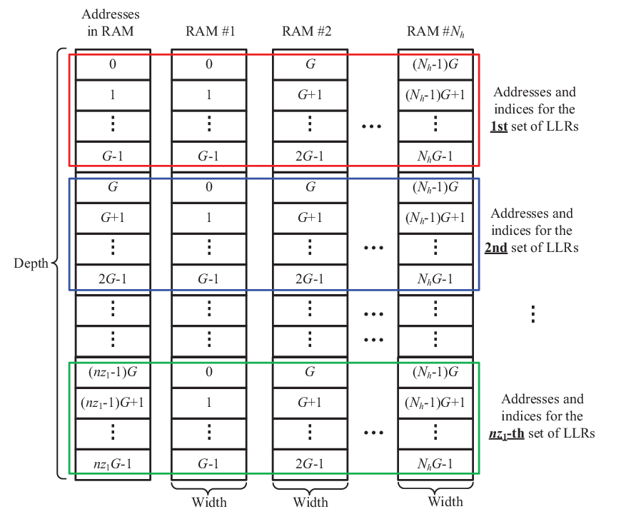
To achieve reading/retrieving data from memories in one clock cycle, we use RAMs to store each type of LLRs, where and is an integer and represents the number of groups. Taking which is related to the P-VNs as an example, each set of LLRs, i.e., a total of LLR values, is further divided into groups. Referring to Fig. 2, the addresses in the RAMs are to store the first set of . In particular, RAM #1 stores the first group of LLRs, i.e., LLRs with indices ; RAM #2 stores the second group of LLRs, i.e., LLRs with indices ; ; and RAM # stores the -th group of LLRs, i.e., LLRs with indices . Using a similar fashion, the addresses in the RAMs are to store the second set of . The arrangement is repeated until all sets of are stored in the RAMs.
With the above storage arrangement, in each clock cycle values from the same LLR set can be retrieved from the RAMs. Using Fig. 2 as an example, at clock the LLR values stored at Address #0 (with indices ) are retrieved; at clock , the LLR values stored at Address #1 (with indices ) are retrieved; ; at clock , the LLR values stored at Address # (with indices ) are retrieved. Thus one set of LLR values (i.e., LLR values) can be retrieved in clock cycles. Hence, reading or writing sets of or for each layer requires clock cycles.
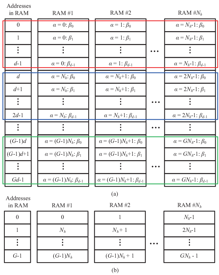
We use a similar storage arrangement for and , which correspond to H-CNs and D1H-VNs, respectively. The only differences are that the RAMs will have different depths and widths. Fig. 3 shows the storage arrangement of and (corresponding to the first layer) in RAMs. In Fig. 3(a), “” () denotes the -th H-CN connected to the -th P-VN; and hence “” to “” represent , i.e., all the P-VNs connected to the -th H-CN. In Fig. 3(b), each address stores the channel LLRs corresponding to the D1H-VNs connected to the same H-CN.
Remark: The aforementioned arrangement of the LLRs in the RAMs is valid regardless of single-port RAMs or dual-port RAMs being used. In other words, no read/write conflicts will occur whether single-port RAMs or dual-port RAMs are used. In the actual hardware implementation, we use dual-port RAMs instead of single-port ones. Since two memory locations in each dual-port RAM can be accessed (read and/or write) at the same time, the number of clock cycles required to read/write one set of LLRs can be further reduced by half compared with the discussion above. The theoretical latency and throughput derived in Sect. III-D and the experimental results shown in Sect. IV are all based on the use dual-port RAMs.
Supposing we have retrieved values for or , we need to interleave them — a process similar to that used in QC-LDPC decoding [36]. For each layer, the exact connections between the H-CNs and the P-VNs are determined by the CPMs, and hence the interleaver can be realized by a simple cyclic shifter. Assuming that the offset value of a CPM equals , we calculate the quotient and the remainder , where denotes the greatest integer less than or equal to and “mod” denotes the modulus operation. When , the corresponding LLRs are cyclically shifted to the left by ; otherwise, these LLRs are cyclically shifted to the left by .

Example: We assume that . Fig. 4(a) shows a identity matrix, i.e., a CPM with ; Fig. 4(b) depicts a CPM with , which can be obtained by cyclically shifting the identity matrix to the right by columns. Assume that the CPM with corresponds to one set of with indices . After retrieving these LLRs from the RAMs and interleaving them, these indices are expected to be re-ordered into . Suppose we use RAMs to store this set of . According to our aforementioned storage scheme, each set of is divided into groups; and each RAM would use the first addresses, i.e., Addresses , to store LLR values. The storage arrangement is shown in Table II. As , we have and . Once the LLRs are retrieved, we process them as follows.
- •
Cyclically shift the LLRs stored at Address #0 (), i.e., LLRs with indices , to the left by and the order of the indices becomes ;
- •
Cyclically shift the LLRs stored at Address #1 () to the left by and the order of the indices becomes ;
- •
Cyclically shift the LLRs stored at Address #2 () to the left by and the order of the indices becomes ;
- •
Cyclically shift the LLRs stored at Address #3 () to the left by and the order of the indices becomes .
Therefore, the expected interleaving effect can be achieved by such a process. Note that the “write” operation can be regarded as the reverse process of the “read” operation. Hence the procedures are similar and are omitted here.
| Address | Indices | |||
|---|---|---|---|---|
| RAM # | RAM # | RAM # | RAM # | |
III-B Operation of A Symbol-MAP Hadamard Sub-decoder
The Hadamard sub-decoder can be considered as the kernel of the PLDPC-HC layered decoder in our implementation and hence will be described in detail. For an order- Hadamard code, the corresponding Hadamard matrices of size can be recursively constructed by
where equals the code length and . Each column of the Hadamard matrices corresponds to a Hadamard codeword, and hence there is a total of codewords in . In (12), we show the Hadamard matrices corresponding to the order- Hadamard code having codewords. Note that the codewords are formed by mapping each in the Hadamard matrices to bit “” and each to bit “”.
| (12) |
When the Hadamard order is even, it has been proven that there always exists a length- single-parity-check (SPC) codeword “embedded” in each Hadamard codeword [27, 31, 32], i.e.,
| (13) | |||||
| (14) |
where the symbol represents the XOR operator. (In (12), the length- SPC constraint is and the corresponding bits are marked in red color.) In each H-CN of the PLDPC-HC described in Section II, the length- SPC codeword is formed by the P-VNs to which the H-CN is connected. Using these bits as inputs to the Hadamard encoder, Hadamard parity-check bits corresponding to the D1H-VNs attached to the H-CN can be generated. (In the case of an order- Hadamard code, bits are input to the Hadamard encoder which generates Hadamard parity-check bits.)
To decode Hadamard codes, a symbol-MAP decoding algorithm has been proposed [27, 31, 32]. We define
| (15) | |||||
| (16) | |||||
| (17) |
as the channel, the a priori and the a posteriori LLR information of the coded bit, respectively. Note that contains only channel observations coming from the D1H-VNs while the remaining values are set to . On the other hand, has non-zero values coming from P-VNs (i.e., repeat decoder) while the remaining values are set to . (Please refer to [31, Section III-B] and [32, Section III-B] for the detailed arrangement of and .) Based on and , is computed using
| (18) |
where represents the a posteriori “information” of the codeword ; and denotes the inner-product operator.


Since the Hadamard matrix has a butterfly-like structure, our Hadamard decoder design is based on the fast Hadamard transform (FHT) block and the dual FHT (DFHT) block [26, 27, 37].
- 1.
We first use a FHT block to compute . Using the structure of the FHT block for shown in Fig. 5 as an example, the inputs are and the outputs are (). Then, is readily obtained from by shifting the least significant bit out. Moreover, is readily available because . There are stages in the FHT block and thus a latency of clock cycles is required.
- 2.
The structure of a DFHT block is similar to that of a FHT block, but with twice the number of inputs and outputs. Using the structure of the DFHT block for shown in Fig. 6 as an example, the inputs to the DFHT block are and ; and the outputs are and (). The module in the DFHT block represents the Jacobian logarithm, i.e.,
where returns the greater value between and . In our design, we use a comparison operation to realize , a look-up-table to realize and an addition operation to sum the above outputs.
As we only need to feedback values related to the information bits, the structure of DFHT block can be further simplified to minimize resources requirement. Same as the FHT block, the DFHT block contains stages and thus has a latency of clock cycles.
Finally, for , it takes another clock cycle to compute
- •
the LLR values which equals
- •
the extrinsic LLR messages which is computed using (7).
Overall, it takes clock cycles to complete one set of computation. Note that the FHT and DFHT blocks have pipeline structures, and the results computed in each stage will be stored in registers. To simplify the presentations of the structures of the FHT block (Fig. 5) and the DFHT block (Fig. 6), we omit all connections to the clock in the figures.
III-C Layered Decoder Architecture
Referring to Fig. 7, we propose an architecture of PLDPC-Hadamard layered decoder based on RAMs and Hadamard sub-decoders. Moreover, we assume that there are Hadamard sub-decoders. In addition to RAMs and sub-decoders, the architecture contains control logics. The control logics are dependent on the structure of the adjacency matrix which has a relatively simple quasi-cyclic format. They are used to ensure that the correct data are loaded into the individual Hadamard sub-decoder and the updated data are written to the correct memory locations 33 3 As can be seen in Fig. 7, one control logic is responsible for reading data from RAMs and loading them to the inputs of the Hadamard sub-decoders while the other control logic is responsible for writing the outputs of the Hadamard sub-decoders to the RAMs. These two control logics can be combined into one, but are shown as two for clarity..

Using the read/write operations described in Section III-A, each set of LLRs, i.e., LLRs or vectors, is first divided into groups and then each group of LLRs is stored in one of the RAMs, where . With this storage method, we can retrieve values of (or ), values of and vectors of from the RAMs in each clock cycle when single-port RAMs are used; and twice the number of LLRs values/vectors when dual-port RAMs are used. Once values of (or ), values of and vectors of are retrieved, the Hadamard sub-decoders can operate on these individual batches of independent data. To ensure that no conflict of memory access occurs during the decoding process, we design the size and storage of RAMs as follows.
- •
RAMs, denoted by PVN-CH-RAM, are used to store . Each RAM has a width of bits (to represent the quantized LLR value) and a depth of . Referring to Fig. 2, the -th location () in the -th RAM () stores where . Note that is needed only once during the first decoding iteration. After the first iteration, the content in PVN-CH-RAM is overwritten by the incoming channel LLR values of the next codeword.
- •
RAMs, denoted by PVN-APP-RAM, are used to store . Each RAM has a width of bits and a depth of . Data are stored in the same way as in PVN-CH-RAM, i.e., the -th location () in the -th RAM () stores where .
- •
RAMs, denoted by H-EX-RAM, are used to store . Each RAM has a width of bits and a depth of . Referring to Fig. 3(a), the -th location () in the -th RAM () stores where , , and .
- •
RAMs, denoted by D1H-CH-RAM, are used to store . Each RAM has a width of bits and a depth of . Each address stores all the channel LLR values for D1H-VNs connected to a H-CN. Referring to Fig. 3(b), the -th location () in the -th RAM () stores where . (To allow the decoding to proceed while receiving the incoming channel LLR values of the next codeword, either two sets of D1H-CH-RAM are used or the depth of D1H-CH-RAM is doubled to . We double the depth of D1H-CH-RAM to in our design.) Moreover, we use dual-port RAMS — one port reads the data in D1H-CH-RAM used for decoding and the other port writes incoming channel LLR values into the same RAM.
III-D Latency and Throughput
III-D1
We first consider a special case in which maximum parallelism is designed for each layer. In other words, we consider the case where and . We also assume dual-port RAMs are used and hence two memory addresses can be accessed at the same time 44 4 Note that single-port RAMs can also be used but then only one memory address can be accessed at one time. The derivations of latency and throughput would be similar to those described in this section but the results would be worse. and it takes clock cycles to retrieve the required sets of (or ) and values in each layer. Note that in (2) is computed in the same clock cycle as (or ) and are retrieved. At the -th clock cycle, we also load the required sets of from one address location to the sub-decoders. Subsequently, LLRs of and vectors of are passed to the FHT blocks in the Hadamard sub-decoders, i.e., LLRs of and one vector of to one FHT block in one Hadamard sub-decoder. Then, it takes clock cycles to compute LLRs of and LLRs of using (7) and (8), respectively. Finally, it takes another clock cycles to write these updated and values into the RAMs.
To summarize,
- i)
Clock cycle no. to : read (or ) and from memory, and at the same time compute using (2);
- ii)
Clock cycle no. (in parallel with above): read ;
- iii)
Clock cycle no. to : process the inputs and by the Hadamard sub-decoders (consisting of FHT and DFHT blocks) using (4);
- iv)
- v)
Clock cycle no. to : write and to memory.
Since , the whole process takes clock cycles.
When , maximum parallelism for each layer is achieved. The latency is minimized and the throughput of the decoder is maximized. However, such a design consumes a lot of hardware resources (a large number of RAMs and Hadamard sub-decoders) and may not be practical. In the next section, we consider the cases when is smaller than .
III-D2
We consider the case when and is an integer. Using the proposed decoder architecture, groups of H-CNs (each consisting of H-CNs) are sequentially processed in each layer. Referring to the timing details in Section III-B and Section III-D1 and with the use of our RAM designs, it takes clock cycles to load the data of one group of H-CNs. (Recall that dual-port RAMs are used.) We use a pipelined structure and load the groups of data to the sub-decoders in a consecutive manner. To complete loading all groups of data, it takes clock cycles. Moreover, the first set of outputs (i.e., and ) is available at the -th clock cycle.


Case I
It means that all the required data are read from the RAMs before the Hadamard sub-decoders generate the updated results. The total time taken to complete updating one layer equals “loading time of all groups + processing time of last group + writing time of last group”, i.e.,
| (20) | |||||
using . Supposing iterations are needed and the clock frequency is , the latency for decoding each codeword equals
| (21) | |||||
where is the number of layers in layered decoding. For a given base matrix, the latency can be reduced by (a) lowering and/or and/or ; or (b) increasing . As the codeword length is , the throughput of the decoder is expressed as
| (22) | |||||
To improve the throughput, we can (a) increase and/or ; or (b) decrease and/or .
Example: Taking , , and as an example, we have and . Fig. 8 shows the timing diagram for the decoding of one layer, in which the LLR data is divided into groups.
- i)
Clock cycle no. to : We load groups of into the Hadamard sub-decoders corresponding to the H-CNs in the layer in clock cycles. In each clock cycle, LLRs of (or ) and LLRs of are read from RAMs, and at the same time LLRs of are computed using (2) and loaded into the Hadamard sub-decoders. Therefore, it takes clock cycles to completely retrieve all LLR values belonging to the first group, i.e., LLRs of (or ) and LLRs of , and to compute and load LLRs of into the Hadamard sub-decoders. Referring to Fig. 8, we use the symbol “1g12” to represent the LLRs corresponding to the first and second P-VNs in Group #1, “1g34” to represent the LLRs corresponding to the third and fourth P-VNs in Group #1, and “1g56” to represent the LLRs corresponding to the fifth and sixth P-VNs in Group #1. Moreover, “g12”, “g34” and “g56” where are defined in a similar fashion. Thus, LLR values belonging to Group #1 are retrieved during Clock cycle no. #1 to #3; Group #2 during Clock cycle no. #4 to #6; Group #3 during Clock cycle no. #7 to #9; and Group #4 during Clock cycle no. #10 to #12.
- ii)
Clock cycle no. , , and : We load groups of into the Hadamard sub-decoders. At clock no. , we load the channel LLRs for D1H-VNs in Group #1 into the Hadamard sub-decoders. Referring to “D1Hch” in Fig. 8, we use the symbol “1gllr” to represent these LLRs in Group #1. Similarly, at clock no. , and , we load the channel LLRs for D1H-VNs in Group #2, Group #3 and Group #4, respectively, into the Hadamard sub-decoders. They are represented by “gllr” in Fig. 8 where 55 5 Note that here for convenience, we use only clock cycle to load one group of into the Hadamard sub-decoders. Thus the four groups of are loaded during clock cycle nos. , , and , leaving some “blank regions” between these clock cycles in Fig. 8 (and also in Fig. 9). Another design is to load each group of using multiple clock cycles (a maximum of 3 clock cycles in this example) so as to minimize the span of the “blank regions”..
- iii)
Clock cycle no. to : We decode one layer consisting of H-CNs in a pipeline manner. At Clock cycle no. , the Hadamard sub-decoders starts processing the LLRs belonging to Group #1 which has completed its LLR loading at Clock cycle no. . Similarly, at Clock cycle no. , and , the Hadamard sub-decoders starts processing the LLRs belonging to Group #2, Group #3 and Group #4, respectively. Since it takes clock cycles to process each group of LLRs and the groups of LLRs are processed in a pipeline manner, the last group of LLRs will be processed completely at Clock cycle no. .
- iv)
Clock cycle no. to : We write the updated groups of data into the corresponding RAMs. Referring to the step above, at Clock cycle no. , , and , the Hadamard sub-decoders starts processing the LLRs belonging to Group #1, Group #2, Group #3 and Group #4, respectively. Moreover, at Clock cycle no. , , and , the Hadamard sub-decoders has completed processing the LLRs belonging to Group #1, Group #2, Group #3 and Group #4, respectively; and has each time generated a group of LLRs consisting of LLR values of and LLR values of . In a similar fashion as in Step i), it takes clock cycles to store/write the LLRs belonging to one group. Thus, LLRs belonging to Group #1 are stored during Clock cycle no. to ; Group #2 stored during Clock cycle no. to ; Group #3 stored during Clock cycle no. to ; Group #4 stored during Clock cycle no. to . In other words, from Clock cycle no. to , updated LLR values of are stored into PVN-APP-RAMs and updated LLR values of are stored to H-EX-RAMs during each clock cycle.
Note that the total time taken to complete updating one layer is clock cycles, which is the same as the theoretical result computed using (20).
Case II
It means that the Hadamard sub-decoders start to output the updated results before all the required data have been read from the RAMs. In this case, we need to use first-in-first-out (FIFO) RAMs to temporarily store the updated results (i.e., and ) from the Hadamard sub-decoders. Once all the required data are read from the RAMs, the updated results stored in the FIFO RAMs are written to the RAMs. The total time taken to complete updating one layer equals “loading time of all groups + writing time of all groups”, i.e.,
| (23) |
The latency to decode one codeword equals
| (24) |
and the throughput equals
| (25) |
which can be improved by (a) increasing and/or ; or (b) decreasing and/or . Fig. 9 shows the timing diagram when decoding one layer with parameters , and . The difference between this case and the previous one is that we use FIFO RAMs to temporarily store the “updated” LLR values until all the required data are loaded into Hadamard sub-decoders.
Note that in both Case I and Case II, it requires clock cycles to complete loading one group of data into the Hadamard sub-decoders. Thus, the Hadamard sub-decoders are idle most of the time 66 6 Note that it is possible to start processing the next layer before the current one is entirely completed. Memory access conflicts as in conventional QC-LDPC decoding architectures will occur but can also be resolved by methods introduced in Sect. I. As this paper mainly focuses on realizing the PLDPC-HC layered decoder and estimates its fixed-point error performance, improving the throughput of the decoder would be left for our future work.. Therefore the throughput can potentially be increased by a factor of if the Hadamard sub-decoders are allowed to process different codewords at the same time. The extra requirement would be times increase in memory storage and a bit more control logics [19].
IV Implementation Results
We implement the and PLDPC-Hadamard decoder (whose base matrix and protograph are shown in Fig. 1) optimized in [31, 32] on the Xilinx VCU118 FPGA board. The maximum operating frequency is MHz 77 7 We start the experiments by setting the clock frequency of the FPGA to MHz. After confirming that the experimental results (i.e., error rates) are the same as those given by fixed-point computer simulations, we continually increase the clock frequency of the FPGA. When the clock frequency exceeds MHz, the experimental results are no longer the same as those given by fixed-point computer simulations. Thus we claim a maximum operating frequency of MHz. and true dual-port RAMs are used. Binary phase-shift-keying (BPSK) modulation and an additive white Gaussian noise channel are assumed. To compare with the floating-point results in [33], we use the same lifting factors, i.e., and , and the same code length .
We implement two designs with () and () Hadamard sub-decoders, respectively, which belong to Case I and Case II in Section III-D. First, we consider the bit-widths setting shown in Fig. 10(a) that has been implemented for both designs. Fig. 11 plots the FER/BER results of the PLDPC-Hadamard code when the number of iterations and . It can be observed that the two designs (i.e., and ) with bit-widths setting produce almost the same FER/BER curves. The minute difference arises only because the same noise samples generated have been assigned to different code bits in the two different designs. The results also show that at a BER of , the fixed-point decoder with bit-widths setting suffers from a degradation of dB compared with the floating-point computation when ; and a degradation of dB when . While no FER/BER error floors appear for the floating-point simulations; for fixed-point results, error floors start to emerge (i) at a BER of (FER around ) for iterations and (ii) at a BER of (FER around ) for iterations.
To investigate the effect of bit-widths setting on the error performance of the fixed-point decoder, we increase the integer part for all the types of LLRs (except for channel observations) in setting by one bit and form the bit-widths setting shown in Fig. 10(b). We implement the setting for the design with Hadamard sub-decoders and plot the FER/BER results in Fig. 11 with iterations. We can observe that increasing the bit-widths can effectively remove the FER/BER error floors when iterations. Based on the setting , we increase the fractional part of (i) output of FHT, (ii) input of DFHT, and (iii) 4 (internal) stages in DFHT, by one bit and form the bit-widths setting . In other words, all the above three categories are represented by 11 bits, i.e., change from “1 sign + 7 int + 2 frac” to “1 sign + 7 int + 3 frac”. We implement the setting for the design with Hadamard sub-decoders and plot the FER/BER results in Fig. 11 with iterations. Comparing the results for setting and those for setting shows that no BER error floor is observed down to (for setting ) and the FER error floor is lowered from (for setting ) to (for setting ).


(a) (b)

Finally, we consider the latency and hardware implementation of the decoders. For (hence ), cycles. When , which belongs to Case I in Section III-D. The decoding latency per layer equals cycles. 88 8 In practice, there is a fixed delay when operating RAMs. In our designs, cycles and are included in deriving the latency and throughput in Table III. Similarly when , which belongs to Case II. The decoding latency per layer equals cycles. Table III lists the hardware implementation results of the proposed layered decoder for () and (). 99 9 The vast majority of the hardware resources are used in (i) storing the LLRs (with BRAMs) and (ii) implementing the parallel Hadamard sub-decoders (with LUTs). The usage of the resources for other purposes is relatively very small. Since the code lengths are identical, the two designs consume almost the same amount of block RAMs (BRAMs). Compared with the decoder with Hadamard sub-decoders and under the same bit widths setting , the one with sub-decoders produces about twice the throughput, reduces the latency by about half, and utilizes about twice the amount of look-up tables (LUTs). For the decoder with sub-decoders, increasing the bit widths from setting to setting increases the LUT utilization from to but does not change the amount of BRAMs used. Note that the hardware utilization of bit widths setting is almost the same as that of bit widths setting and is therefore not shown in Table III.
|
||||||
|
||||||
|
||||||
|
() | () | ||||
|
() | () | ||||
|
NA | () | ||||
|
NA | () | ||||
|
||||||
|
dB | dB | dB | dB | ||
| Latency | ms | ms | ms | ms | ||
|
Gbps | Gbps | Gbps | Gbps | ||
V Conclusion
A hardware architecture of the PLDPC-Hadamard layered decoder has been designed and implemented onto an FPGA. The architecture consists of control logics, BRAMs and Hadamard sub-decoders. The latency and throughput of the design have been derived in the terms of the code parameters and the amount of parallel sub-decoders deployed. A throughput of Gbps is achieved when decoding iterations are used. Moreover, increasing the bit widths of the data in the decoder has shown to be an effective way of eliminating/lowering the FER/BER error floors.
In our current decoder design, the Hadamard sub-decoders are not fully utilized in the time domain. When these sub-decoders are fully utilized, the decoder can decode ( in the example used) codewords simultaneously and hence increase the throughput by the same factor (i.e., to almost Gbps). To decode more codewords, more BRAMs would be needed though. Our decoder architecture is generic and can be readily modified to decode LDPC-Hadamard codes with the order of the Hadamard code being odd, i.e., is odd. Moreover, it can be modified and applied to decode other LDPC-derived codes when the Hadamard constraints LDPC-HC are replaced by other code constraints.
To eliminate/lower the error floors, we have increased the bit widths in our decoder design. Another future direction of research is to design variable bit widths (i.e., quantization schemes) in the decoder [38] so as to reduce the complexity of the decoder and to remove the error floor issue.
References
- [1] C. Berrou, A. Glavieux, and P. Thitimajshima, “Near Shannon limit error-correcting coding and decoding: Turbo-codes,” in Proc. IEEE Int. Conf. Commun. (ICC), vol. 2, pp. 1064–1070, May 1993.
- [2] R. G. Gallager, Low-Density Parity-Check Codes. PhD thesis, MIT Press, Cambridge, USA, 1963.
- [3] D. Divsalar, H. Jin, and R. McEliece, “Coding theorems for turbo-like codes,” in Proc. Allerton Conf., pp. 201–210, 1998.
- [4] T. J. Richardson, M. A. Shokrollahi, and R. L. Urbanke, “Design of capacity-approaching irregular low-density parity-check codes,” IEEE Trans. Inf. Theory, vol. 47, no. 2, pp. 619–637, Feb. 2001.
- [5] M. F. Brejza, L. Li, R. G. Maunder, B. M. Al-Hashimi, C. Berrou, and L. Hanzo, “20 years of turbo coding and energy-aware design guidelines for energy-constrained wireless applications,” IEEE Commun. Surv. Tut., vol. 18, no. 1, pp. 8–28, 2016.
- [6] A. Ardakani and M. Shabany, “A novel area-efficient VLSI architecture for recursion computation in LTE turbo decoders,” IEEE Trans. Circuits Syst. II, Exp. Briefs, vol. 62, no. 6, pp. 568–572, 2015.
- [7] Y. Liu, P. M. Olmos, and D. G. M. Mitchell, “On generalized LDPC codes for 5G ultra reliable communication,” in Proc. 2018 IEEE Inf. Theory Workshop (ITW), pp. 1–5, 2018.
- [8] Y. Fang, G. Han, G. Cai, F. C. M. Lau, P. Chen, and Y. L. Guan, “Design guidelines of low-density parity-check codes for magnetic recording systems,” IEEE Commun. Surv. Tut., vol. 20, no. 2, pp. 1574–1606, 2018.
- [9] Z. W. Li, L. Chen, L. Q. Zeng, S. Lin, and W. H. Fong, “Efficient encoding of quasi-cyclic low-density parity-check codes,” IEEE Trans. Commun., vol. 52, no. 4, pp. 670–678, Apr. 2004.
- [10] C.-C. Cheng, J.-D. Yang, H.-C. Lee, C.-H. Yang, and Y.-L. Ueng, “A fully parallel LDPC decoder architecture using probabilistic min-sum algorithm for high-throughput applications,” IEEE Transactions on Circuits and Systems I: Regular Papers, vol. 61, no. 9, pp. 2738–2746, 2014.
- [11] M. Zhao, X. Zhang, L. Zhao, and C. Lee, “Design of a high-throughput QC-LDPC decoder with TDMP scheduling,” IEEE Trans. Circuits Syst. II, Exp. Briefs, vol. 62, no. 1, pp. 56–60, 2015.
- [12] Y. Lee, M. Li, and L. Van der Perre, “Memory-reduced turbo decoding architecture using NII metric compression,” IEEE Trans. Circuits Syst. II, Exp. Briefs, vol. 63, no. 2, pp. 211–215, 2016.
- [13] P. Hailes, L. Xu, R. G. Maunder, B. M. Al-Hashimi, and L. Hanzo, “A survey of FPGA-based LDPC decoders,” IEEE Commun. Surv. Tut., vol. 18, no. 2, pp. 1098–1122, 2016.
- [14] J. Thorpe, “Low-density parity-check (LDPC) codes constructed from protographs,” in Proc. IPN Progr. Rep., pp. 1–7, Aug. 2003.
- [15] Y. Fang, G. A. Bi, Y. L. Guan, and F. C. M. Lau, “A survey on protograph LDPC codes and their applications,” IEEE Commun. Surv. Tut., vol. 17, no. 4, pp. 1989–2016, 2015.
- [16] K. Zhang, X. Huang, and Z. Wang, “A high-throughput LDPC decoder architecture with rate compatibility,” IEEE Trans. Circuits Syst. I, Reg. Papers, vol. 58, no. 4, pp. 839–847, 2011.
- [17] C. Marchand, J.-B. Dore, L. Conde-Canencia, and E. Boutillon, “Conflict resolution for pipelined layered LDPC decoders,” in 2009 IEEE Workshop on Signal Processing Systems, pp. 220–225, 2009.
- [18] Y. Sun and J. R. Cavallaro, “VLSI architecture for layered decoding of QC-LDPC codes with high circulant weight,” IEEE Transactions on Very Large Scale Integration (VLSI) Systems, vol. 21, no. 10, pp. 1960–1964, 2013.
- [19] S. Kumawat, R. Shrestha, N. Daga, and R. Paily, “High-throughput LDPC-decoder architecture using efficient comparison techniques & dynamic multi-frame processing schedule,” IEEE Transactions on Circuits and Systems I: Regular Papers, vol. 62, no. 5, pp. 1421–1430, 2015.
- [20] Q. Lu, J. Fan, C. Sham, W. M. Tam, and F. C. M. Lau, “A 3.0 Gb/s throughput hardware-efficient decoder for cyclically-coupled QC-LDPC codes,” IEEE Trans. Circuits Syst. I, Reg. Papers, vol. 63, no. 1, pp. 134–145, 2016.
- [21] H.-C. Lee, M.-R. Li, J.-K. Hu, P.-C. Chou, and Y.-L. Ueng, “Optimization techniques for the efficient implementation of high-rate layered QC-LDPC decoders,” IEEE Trans. Circuits Syst. I, Reg. Papers, vol. 64, no. 2, pp. 457–470, 2017.
- [22] O. Boncalo, G. Kolumban-Antal, A. Amaricai, V. Savin, and D. Declercq, “Layered LDPC decoders with efficient memory access scheduling and mapping and built-in support for pipeline hazards mitigation,” IEEE Transactions on Circuits and Systems I: Regular Papers, vol. 66, no. 4, pp. 1643–1656, 2019.
- [23] V. L. Petrovic, M. M. Markovic, D. M. E. Mezeni, L. V. Saranovac, and A. Radosevic, “Flexible high throughput QC-LDPC decoder with perfect pipeline conflicts resolution and efficient hardware utilization,” IEEE Transactions on Circuits and Systems I: Regular Papers, vol. 67, no. 12, pp. 5454–5467, 2020.
- [24] M. Li, V. Derudder, K. Bertrand, C. Desset, and A. Bourdoux, “High-speed LDPC decoders towards 1 Tb/s,” IEEE Trans. Circuits Syst. I, Reg. Papers, vol. 68, no. 5, pp. 2224–2233, 2021.
- [25] A. Verma and R. Shrestha, “Hardware-efficient and high-throughput LLRC segregation based binary QC-LDPC decoding algorithm and architecture,” IEEE Transactions on Circuits and Systems II: Express Briefs, vol. 68, no. 8, pp. 2835–2839, 2021.
- [26] L. Ping, W. K. Leung, and K. Y. Wu, “Low-rate turbo-Hadamard codes,” IEEE Trans. Inf. Theory, vol. 49, no. 12, pp. 3213–3224, Dec. 2003.
- [27] G. Yue, L. Ping, and X. Wang, “Generalized low-density parity-check codes based on Hadamard constraints,” IEEE Trans. Inf. Theory, vol. 53, no. 3, pp. 1058–1079, 2007.
- [28] D. J. Costello and G. D. Forney, “Channel coding: The road to channel capacity,” Proc. IEEE, vol. 95, no. 6, pp. 1150–1177, 2007.
- [29] W. K. R. Leung, G. Yue, L. Ping, and X. Wang, “Concatenated zigzag Hadamard codes,” IEEE Trans. Inf. Theory, vol. 52, no. 4, pp. 1711–1723, 2006.
- [30] L. Ping, L. Liu, Keying Wu, and W. K. Leung, “Interleave division multiple-access,” IEEE Trans. Wireless Commun., vol. 5, no. 4, pp. 938–947, 2006.
- [31] P. W. Zhang, F. C. M. Lau, and C.-W. Sham, “Protograph-based low-density parity-check Hadamard codes,” https://arxiv.org/abs/2010.08285, 2020.
- [32] P.-W. Zhang, F. C. M. Lau, and C.-W. Sham, “Protograph-based LDPC Hadamard codes,” IEEE Trans. Commun., vol. 69, no. 8, pp. 4998–5013, 2021.
- [33] P. W. Zhang, F. C. M. Lau, and C.-W. Sham, “Layered decoding for protograph-based low-density parity-check Hadamard codes,” IEEE Commun. Lett., vol. 25, no. 6, pp. 1776–1780, 2021.
- [34] Y. Wang, S. C. Draper, and J. S. Yedidia, “Hierarchical and high-girth QC-LDPC codes,” IEEE Trans. Inf. Theory, vol. 59, no. 7, pp. 4553–4583, 2013.
- [35] M. Fossorier, “Quasi-cyclic low-density parity-check codes from circulant permutation matrices,” IEEE Trans. Inf. Theory, vol. 50, no. 8, pp. 1788–1793, Aug. 2004.
- [36] C.-W. Sham, X. Chen, F. C. M. Lau, Y. Zhao, and W. M. Tam, “A 2.0 Gb/s throughput decoder for QC-LDPC convolutional codes,” IEEE Trans. Circuits Syst. I, Reg. Papers, vol. 60, no. 7, pp. 1857–1869, 2013.
- [37] S. Jiang, P. W. Zhang, F. C. M. Lau, and C.-W. Sham, “An ultimate-Shannon-limit-approaching Gbps throughput encoder/decoder system,” IEEE Trans. Circuits Syst. II, Exp. Briefs, vol. 67, no. 10, pp. 2169–2173, 2020.
- [38] X. Zhang and P. H. Siegel, “Quantized iterative message passing decoders with low error floor for LDPC codes,” IEEE Transactions on Communications, vol. 62, no. 1, pp. 1–14, 2014.
![[Uncaptioned image]](2110.07906v2/zpw_bio.png) |
Peng-Wei Zhang received the Bachelor of Engineering degree in Electronics and Information Engineering and the Master of Engineering degree in Electronics and Communication Engineering from Chongqing University of Posts and Telecommunications, China, in 2013 and 2016, respectively. He received his PhD degree at the Department of Electronic and Information Engineering, The Hong Kong Polytechnic University, Hong Kong SAR, China, in 2021. He is now with Huawei Technologies Ltd., Chengdu, China. |
![[Uncaptioned image]](2110.07906v2/sheng.png) |
Sheng Jiang received the Bachelor of Engineering Degree in Microelectronics from Shanghai Jiaotong University, China; Master of Engineering Degree in Electronic Engineering from Hong Kong University of Science and Technology, Hong Kong; and PhD Degree from The Hong Kong Polytechnic University, Hong Kong. He is currently a postdoctoral fellow at The Hong Kong Polytechnic University, Hong Kong. |
![[Uncaptioned image]](2110.07906v2/FCMLau-photo.png) |
Francis C. M. Lau received the BEng(Hons) degree in electrical and electronic engineering and the PhD degree from King’s College London, University of London, UK. He is a Professor at the Department of Electronic and Information Engineering, The Hong Kong Polytechnic University, Hong Kong. He is also a Fellow of IEEE and a Fellow of IET. He is a co-author of two research monographs. He is also a co-holder of six US patents. He has published more than 330 papers. His main research interests include channel coding, cooperative networks, wireless sensor networks, chaos-based digital communications, applications of complex-network theories, and wireless communications. He is a co-recipient of one Natural Science Award from the Guangdong Provincial Government, China; eight best/outstanding conference paper awards; one technology transfer award; two young scientist awards from International Union of Radio Science; and one FPGA design competition award. He was the General Co-chair of International Symposium on Turbo Codes & Iterative Information Processing (2018) and the Chair of Technical Committee on Nonlinear Circuits and Systems, IEEE Circuits and Systems Society (2012-13). He served as an associate editor for IEEE TRANSACTIONS ON CIRCUITS AND SYSTEMS II (2004-2005 and 2015-2019), IEEE TRANSACTIONS ON CIRCUITS AND SYSTEMS I (2006-2007), and IEEE CIRCUITS AND SYSTEMS MAGAZINE (2012-2015). He has been a guest associate editor of INTERNATIONAL JOURNAL AND BIFURCATION AND CHAOS since 2010. |
![[Uncaptioned image]](2110.07906v2/Bruce.png) |
Chiu-Wing Sham received his Bachelor degree (Computer Engineering) and MPhil. degree from The Chinese University of Hong Kong in 2000 and 2002 respectively, and received his Ph.D. degree from the same university in 2006. He has worked as an Electronic Engineer on the FPGA applications of the motion-control system and system security with cryptography in ASM Pacific Technology Ltd (HK). During the years at The Hong Kong Polytechnic University, he engaged in various University projects for the commercialization of technology, in particular, a few optical communication projects which were in collaboration with Huawei. He also worked on the physical design of VLSI design automation. He was invited to work at Synopsys, Inc. (Shanghai) in the summer of 2005 as a Visiting Research Engineer. He is now working at The University of Auckland as a Senior Lecturer. He is also an IEEE Senior Member and an Associate Editor of IEEE TRANSACTIONS ON CIRCUITS AND SYSTEMS II (2017-present). |