Aligned Stacking of Nanopatterned 2D materials – Towards 3D printing at atomic resolutionjonas.haas@uni-tuebingen.dejannik.meyer@uni-tuebingen.de
Abstract
Two-dimensional materials can be combined by placing individual layers on top of each other, so that they are bound only by their van der Waals interaction. The sequence of layers can be chosen arbitrarily, enabling an essentially atomic-level control of the material and thereby a wide choice of properties along one dimension. However, simultaneous control over the structure in the in-plane directions is so far still rather limited. Here, we combine spatially controlled modifications of 2D materials, using focused electron irradiation or electron beam induced etching, with the layer-by-layer assembly of van der Waals heterostructures. A novel assembly process makes it possible to structure each layer with an arbitrary pattern prior to the assembly into the heterostructure. Moreover, it enables a stacking of the layers with accurate lateral alignment, with an accuracy of currently 10nm, under observation in an electron microscope. Together, this enables the fabrication of almost arbitrary 3D structures with highest spatial resolution.
Keywords: 2D materials, van der Waals heterostructures, nanopatterning, electron microscopy, nanoscale assembly, 3D printing
1 Introduction
Structuring matter on the smallest dimensions is a key capability for many areas of technology, most prominently for information processing but also for sensing, nanofluidics, optics, catalysis, medicine and many more [1, 2, 3, 4, 5, 6]. As an observation that has become known as Moore’s law [7, 8], the feature sizes in information processing devices have continuously shrunk over many decades, now approaching limitations given by the granularity of the atomic structure. However, current computing devices are essentially planar. Methods for generating arbitrary 3D structures are commonly referred to as ”3D printing”. Also in this area, the minimum feature sizes that can be defined are continuously shrinking as new approaches are invented and developed, although the 3D resolution is still larger than what can be achieved in planar structures [9, 10, 11, 12, 13, 14]. Currently, optical methods can be pushed to a resolution of about 100nm [12]. Electron- or ion-beam induced deposition can reach a resolution in the nanometer-range for planar structures on thin membranes [15], but generally the resolution is limited by the interaction volume rather than the beam diameter, which also depends on the target geometry, and for 3D structures is typically in the range of tens of nanometers [11]. Another important aspect for 3D printing techniques is the (often rather limited) choice of the materials that can be integrated with each other for fabricating functional devices [16].
Two-dimensional materials (2D materials) are isolated, one unit cell (or half a unit cell) thick layers, most of which can be described as an individual plane extracted from a van der Waals bonded layered material [17, 18, 19, 20, 21]. Some of them are only one atom thick (e.g. graphene or single-layer hexagonal boron nitride), while many more examples can be given for structures with two, three or more atomic layers. Importantly, these layers can be assembled in any arbitrary sequence, yielding so-called van der Waals (vdW) heterostructures [22, 23, 24, 25, 20, 26, 27, 21, 28, 29, 30, 31, 32]. This allows combining unique properties of the constituents, and may also lead to entirely new features due to the interaction between the layers. For example, hexagonal boron nitride (hBN) is not only an excellent substrate for graphene [33], but can also have a profound influence on graphene’s electronic properties that sensitively depends on the relative alignment [34, 35] of the sheets. The assembly of conducting (e.g. graphene), insulating (e.g. hBN) and semiconducting layers (e.g. molybdenum disulfide, MoS2) has led to a wide range of new device geometries such as transistors with ultra-thin gate dielectric [36], tunneling transistors [23], memory devices [37], oscillators [38], photo-transistors[39] and photo-voltaic devices [40]. Modifications of the electronic structure often rely on Moiré effects or other naturally occurring short-range periodicities [41], with a prominent example being the superconductivity observed in graphene bilayers with a magical misorientation angle of 1.1° [42]. Moiré lattice potentials provide an easy access to periodic variations in the few-nm range, however, they can not be directly used to fabricate more complex potential landscapes. Besides electronic and optical applications, vdW heterostructures are important for molecular sieves [43], nanopores [44], catalysis [45], or nanoscale liquid cells [46], just to name a few.
2D materials can be structured by conventional lithographic techniques, after they are deposited on a substrate [47, 48]. However, much higher resolution can be achieved if 2D materials are available as free-standing membranes: In particular, the direct cutting of graphene [49, 50, 51, 52], other 2D materials [53, 54], or complete vdW heterostructures [55, 56] by the focused electron beam in a transmission electron microscope (TEM) or scanning transmission electron microscope (STEM) makes it possible to define feature sizes in the nanometer range. Similarly, electron-beam induced etching (EBIE) [57, 58] or cutting of 2D materials by ion beams [59, 60] is preferentially done with free-standing membranes. Individual impurity atoms in graphene membranes can even be relocated to specific atomic sites [61, 62, 63], enabling a true atomic-level control, comparable to the relocation of atoms on surfaces using scanning tunneling microscopy [64]. However, again these structures are limited to two dimensions, and the integration with other materials, e.g. additional nanostructured layers, is not straightforward.

In this work, we developed an approach that combines the almost-atomic resolution structure definition in free-standing 2D material membranes with the assembly of pre-structured layers into van der Waals heterostructures. Fig. 1 schematically illustrates the idea: A structure is defined in every one- or few-atom thin layer, and the layers are placed on top of each other with a precise lateral alignment. The concept can be categorized as 3D printing, which (in most of its implementations) also proceeds by forming a target structure layer by layer. Critically, the lateral alignment between the layers must be of a similar accuracy than the targeted resolution. Here, we repeatedly achieve an accuracy of 10nm, although this is probably not a fundamental limitation of the approach. We also point out that the material for each layer can in principle be chosen from the vast repertoire of available 2D materials, which should make it possible to directly create functional devices.
2 Experiments and Results
2.1 General considerations
To enable structured modifications by focused electron irradiation at highest resolution, it is essential that the individual layers are free-standing at this step, which is prior to the stacking. Similarly, it is important that the aligned stacking is done with visual feedback from an electron microscope, hence it has to be done in a vacuum (using nano-manipulators). These requirements are in conflict with previously published methods for the deterministic transfer of 2D materials and their assembly into heterostructures [26, 27, 28, 29, 30, 31, 32], all of which employ a transfer medium in contact with the layers, and in some cases a chemical removal of the transfer layer. The concept of our layer transfer is schematically shown in Fig. 2: We start with a 2D material layer as free-standing membrane, attached to a relatively large support frame (10µm diameter in our case). Into this membrane, a pattern is written using focused electron irradiation in the (S)TEM, or by EBIE in the scanning electron microscope (SEM). The membrane is brought into contact with a second, smaller support frame. The surface around this second hole is curved, to facilitate a contact at the desired area in spite of unavoidable small tilt between the two frames. Upon contact, the 2D material membrane sticks to the surface of the smaller support frame, and spans the hole in this frame. Importantly, this adhesion is strong enough that the material can be detached from the initial frame: By moving the initial support frame slightly sideways (black arrows in Fig. 2d), the material breaks off from this frame around the edges (red arrows in Fig. 2d). Now, the process can be repeated with the next layer (Fig. 2f-j).

2.2 Implementation
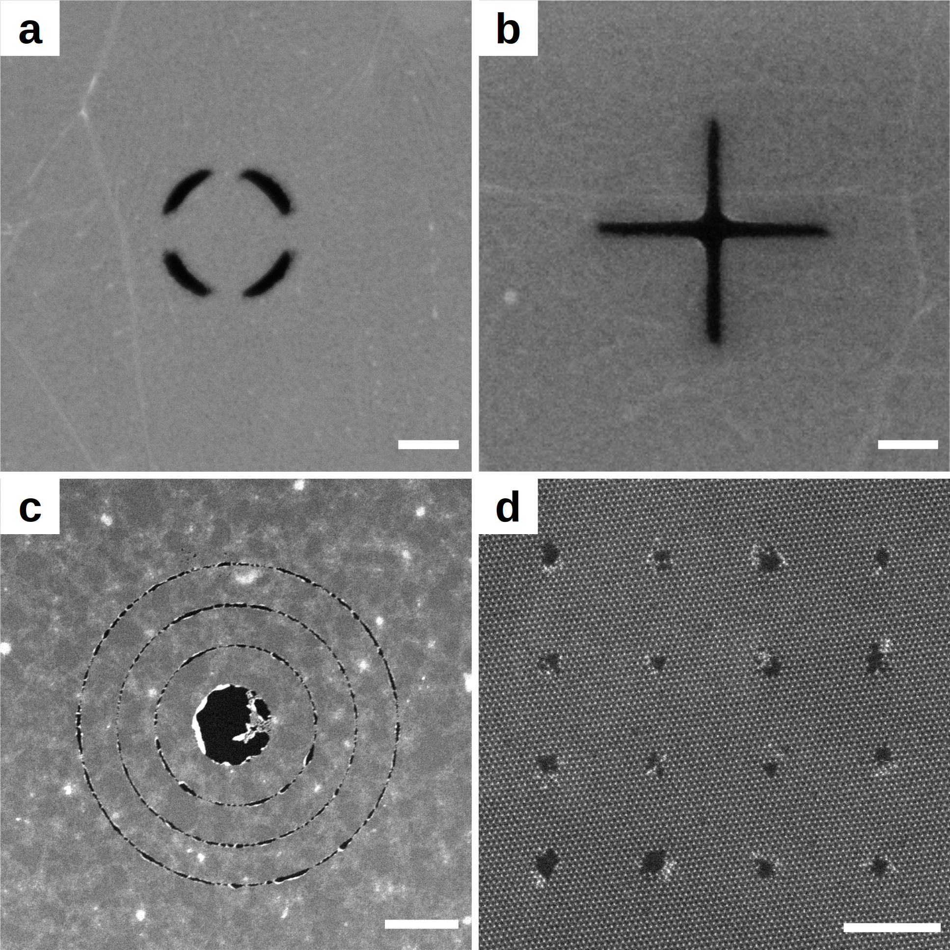
After introducing the concept, we now show the practical implementation. So far, we have prepared stacks of patterned Tungsten disulfide (WS2), Molybdenum disulfide (MoS2), and graphene. These 2D materials are prepared into free-standing membranes, and patterns are written into the membranes. For writing patterns into the WS2 or MoS2, we used a 200kV electron beam in a (S)TEM. For graphene, we alternatively use EBIE for removing material in a controlled pattern. This is done using a 3kV electron beam in a scanning electron microscope in presence of water vapor (see methods for details). While EBIE has less spatial resolution than sputtering at high voltages, it requires less time for structuring larger areas. Moreover, it simplifies the process as it can be done in the same device as the stacking. Fig 3 shows exemplary free-standing membranes patterned by EBIE and STEM, respectively.
Now we turn to the most critical aspect of placing and stacking the 2D materials with precise lateral alignment. An illustration of the experimental setup with the manipulation stages, which is used to carry out the presented process (except for patterning individual layers) is shown in Fig. 4a. The individual layers are attached to a TEM grid, cut into one quarter. The target substrate is made from one of the fingers in a FIB lift-out grid, by making it more narrow, making it thinner, and inserting a hole. This is done by FIB, prior to placing the 2D materials, as shown in the supplementary information. For accurate alignment, the suspended, pre-structured layers on the TEM grid are held in a nanomanipulator which is attached to the SEM chamber. The target substrate is mounted on the six-axis SEM stage.
A schematic image sequence of the process is shown in Fig. 4a-f. First, the grid is brought above the target substrate, such that the free-standing membrane is centered on the hole in the target (see Fig. 4b-d). Now, the target substrate is moved upwards until a contact is made. The contact can be noticed by a clear change in contrast as illustrated in Fig. 4e. Slight lateral motion of the TEM grid leads to a rupture of the 2D material at the edge of its connection to the TEM grid. Breaking points, as shown in Fig. 4c-f as circular cutouts, can be introduced (already during patterning) to promote tearing-off. Now, the TEM grid can be moved upwards, leaving the membrane placed into the desired specific location on the target substrate (Fig. 4f).
Fig. 4g-l shows an SEM image sequence of placing one graphene membrane. A close-up of the target substrate is shown in Fig. 4h, while Fig. 4i shows the membrane into which a hole was cut by EBIE suspended on the TEM grid. The grid is brought close to the target substrate, such that the hole in the graphene is centered on the hole in the target. As described above, the membrane is placed by bringing the membrane and the target in contact, notably by a change in the SEM image contrast (see Fig. 4j vs. Fig. 4k and video in supplement). Now, the membrane is torn off by slight lateral motions. Importantly, this motion does not cause any displacement of the membrane with respect to the substrate as their adhesion is strong enough, but only rupturing from the TEM grid at the predetermined breaking points. Fig. 4l shows the graphene layer after placement on the target substrate. This process is repeated for placing additional layers onto the first one. A video showing the aligned stacking of two patterned graphene layers is given in the supplement.

Since the 2D materials are semi-transparent in SEM, features in both layers can be observed during placement of a layer, and hence an accurate alignment using the nanomanipulator is possible. It is worth noting that this applies both to the exact alignment of the membranes to each other as well as of the membranes on the substrate itself. While the layers are still at a distance, they can also be distinguished by the difference in focus height of the SEM (see supplementary video). For rough alignment, the secondary electron (SE) or the Inlens-SE detector of the SEM can be used. The combination of the Inlens-SE detector with a STEM detector, however, facilitates the observation of features in the already deposited layers for an accurate alignment. Figure 5 and Figure 6 show SEM and TEM images of layer structures prior to stacking and after stacking.
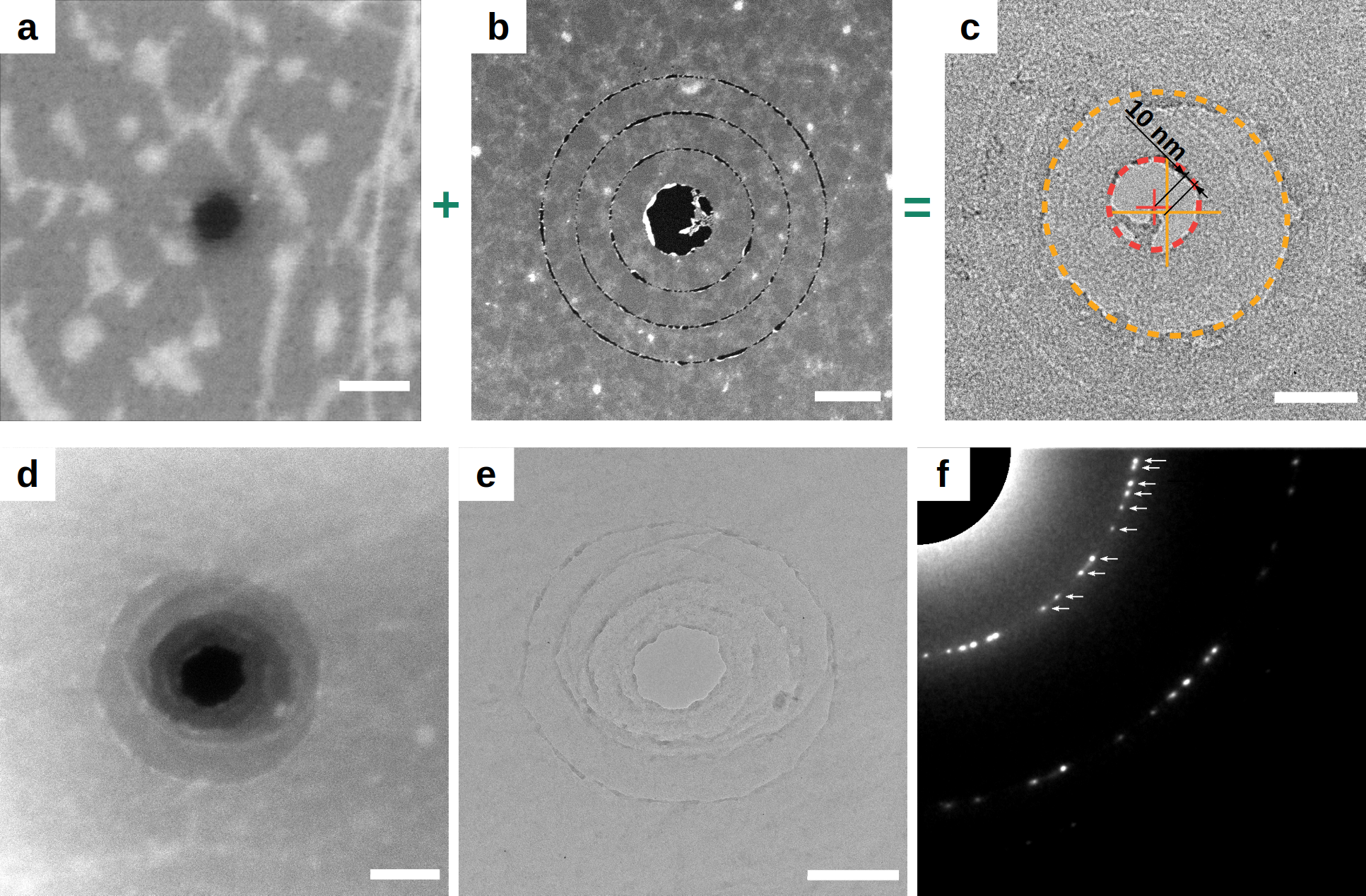
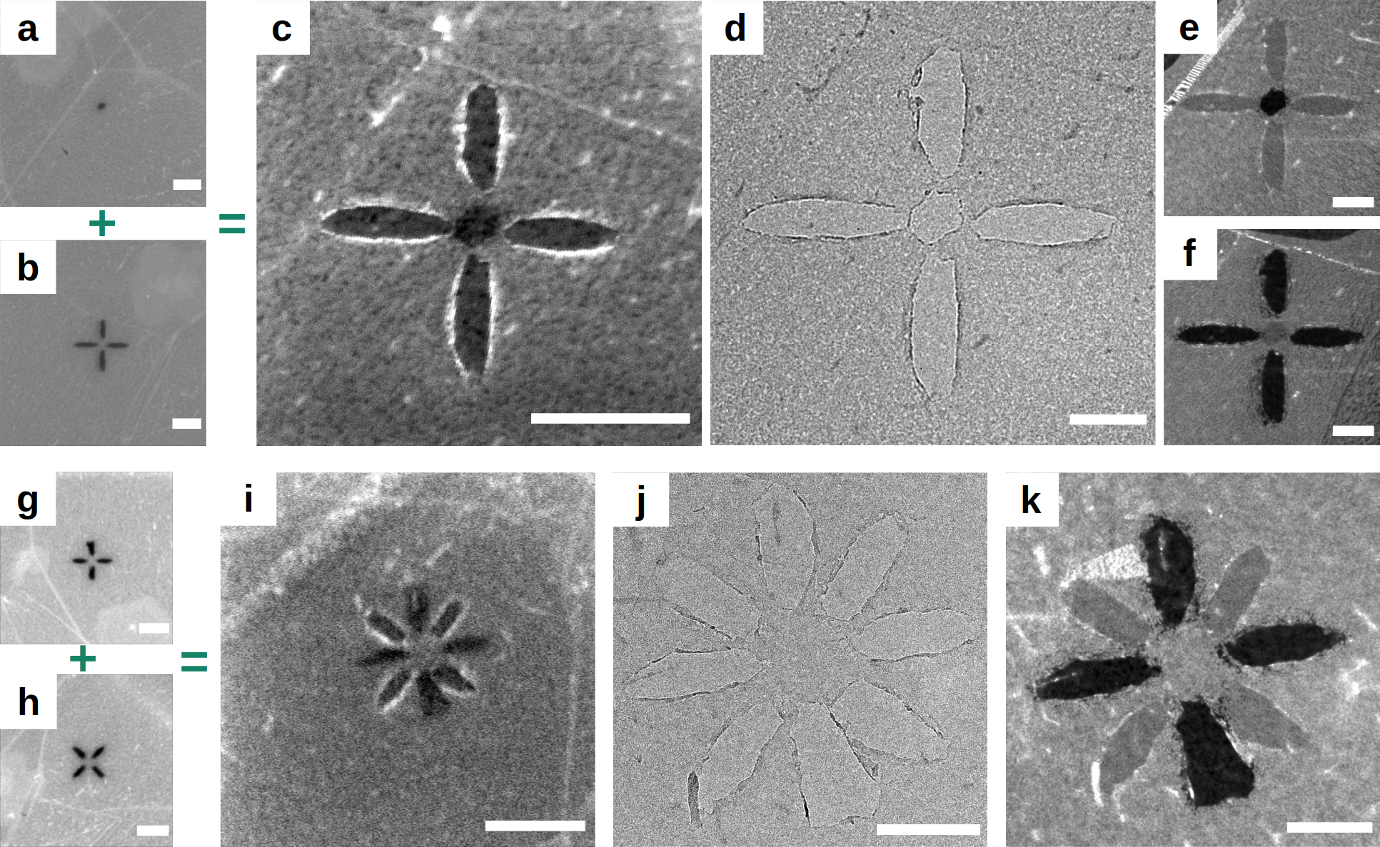
In order to assess the accuracy of the lateral alignment, we analyze the offset between the patterns of the membranes in the final assembled structure. For this purpose, we measure the distance between the centers of the hole patterns, as exemplified in Figure 5c. Here, the offset between the hole in graphene and the hole in MoS2 is displaced by about . For the assembly of the ten graphene layers (see Figure 5 d-f), the average offset was , with a minimum of and a maximum of (see also Figure S2 in the supplement).
2.3 Integrating non-contiguous layer structures
For many types of 3D printing, a limitation of the possible structures arises from the requirement that the structures must be stable at any time during the fabrication, i.e., already when the structure is only partly finished. In the approach as described so far, even every layer must be stable by itself (as it is separately transferred), which means it can not contain isolated blocks of the material.
To our surprise, however, it turns out that even structures that contain isolated blocks of material can be written into the TMDs, resulting in a ”nearly” free-standing structure held only by very thin, disordered residue of material. Some examples are shown in Fig. 7: Depending on the sequence of writing the pattern, the isolated block of the TMD may remain at its original position, or may shift to one side. However, we have never observed that the isolated block of the TMD materials disappeared entirely. In Fig. 7b, the remaining structure is only supported by a few atom thick strings, which appear to be similar to the wires between beam-induced holes of Ref. [65, 66]. Indeed, as noted already in [65, 66], these wires are much more resistant to damage from the electron beam than the original TMD lattice. Hence, the process of cutting isolated blocks into TMDs becomes self-limiting at the point where the structure is only hanging on few-atom thick wires of the TMD, and thus can be reproduced reliably. For graphene, in this example structured by EBIE, it is similarly possible to create almost-disconnected pieces of material (Fig. 7c). However, in this case, the electron dose must be carefully balanced. Pieces of graphene that are disconnected from the support tend to fold up or adhere next to the hole (supplementary Fig. S3).
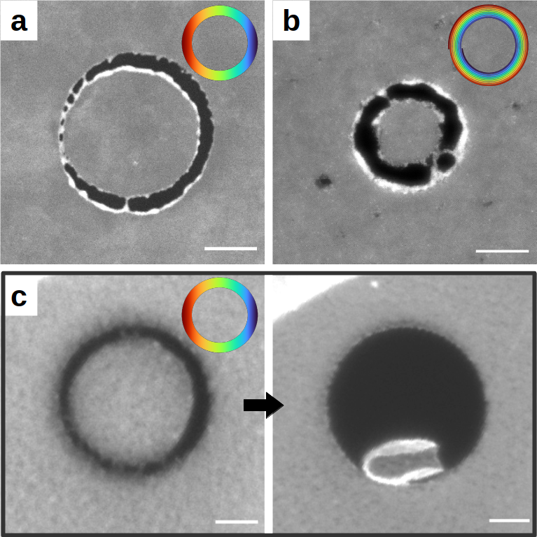
Even delicate structures as in Fig. 7b, where a piece of material is only attached by atomic-scale wires, can be assembled into a stack. This is exemplified in Fig. 8. After patterning, the almost-isolated WS2 quantum dot is stacked on top of another WS2 membrane. Fig. 8b shows the resulting structure. To illustrate the individual layers, Fourier filtering is used to highlight the two different lattice orientations in the atomically resolved image. As shown in Fig. 8b, one of the layers is continuous, while the other layer contains an isolated disc of WS2.

3 Discussion
The methods developed in this work enable the fabrication of novel nanostructures and device geometries on the basis of 2D materials. In particular, the aligned stacking of pre-patterned layers extends the existing capabilities for in-plane structuring into the third dimension. Although only three different materials were tested so far, the basic approach can be expected to work with a large variety of 2D materials and possibly other thin layers.
Structuring within each layer can be performed with nearly atomic precision, as evidenced in Fig 3d, and also in prior works [49, 50, 51, 52, 53, 54, 55, 56]. We also note that the lattice structure of the WS2 is practically unaffected outside of the holes that were defined by the focused electron beam. When structuring TMDs by focused, high-energy electron irradiation, we found that one can create isolated blocks of material that are only held in place by a few atomic-scale wires through a self-limiting process. This could be useful to create quantum dot structures out of these materials, or other types of isolated elements in the future.
Stacking of 2D material layers naturally generates an atomic level precision along the third dimension, via the choice of the material, and here also via the potential introduction of gaps in the chosen layers. In this respect, it should be pointed out that in both TEM and SEM imaging of 2D materials, some amount of amorphous carbon is deposited on the 2D materials. This amorphous carbon likely stems from hydrocarbons adsorbed on the sample surfaces which are cracked under electron irradiation. With our experiments carried out in standard TEM and SEM instruments, it is inevitable that these hydrocarbon deposits are also present in the 2D material stacks, including between the layers. Amorphous carbon as formed under an electron beam is not mobile enough to be pushed into pockets of the heterostructure, unlike other contaminants [24, 67]). Further improvements to avoid this contamination, by carrying out the stacking in an ultra-high vacuum SEM and structuring the sample at elevated temperature, are currently being set up.
The largest remaining uncertainty in the spatial control over the 3D structure is the accuracy in the lateral alignment of the layers. We regularly achieve an alignment accuracy of about 10nm, which is slightly less than what one would expect considering the resolution of the SEM of 2-3nm. The reason is that, currently, the alignment of the layers to each other is only visually estimated by the user while stacking: during the continuous upward movement of the substrate on the Z-stage, the alignment is verified by adjusting the focus to different heights, and corrected using the nanomanipulator if necessary. In addition, a short pixel time must be selected to observe the process in real time, resulting in rather noisy images. We expect that this could be significantly improved by measuring the offset in the SEM image, e.g. by automated pattern recognition. An additional practical complication when using the SEM stage is a non-perfect decoupling of in-plane (x,y) and height (z) direction, e.g. a jump in (x,y) when inverting the z drive direction. In principle, we see no reason why the accuracy in the lateral alignment couldn’t be pushed to the resolution of the observing electron microscope, or even beyond – indeed, measuring the center position of a given reference feature should be possible with a higher accuracy than the resolution of the underlying image.
The twist angle between features in different layers can also be considered as part of the in-plane alignment. As shown in Fig. 6g-k, the orientation of the two crosses could be made at the desired relative angle of 45 degrees. This is achieved by patterning the two layers into different locations on the same grid containing the source material (prior to stacking), and then, relative orientation of the features as defined during writing is maintained. Rotation of the target is also possible, but was not used so far.
In this work, we have stacked up to ten layers, with lateral dimensions of the features in the order of 100nm in diameter. This corresponds to a build volume of ca. . With the manual preparation, structuring and placement, the time needed to create this assembly is ca. 8 hours, resulting in a build speed of ca. . However, most of this time is used for loading samples into a device, for microscope alignment, and similar steps. If we consider only the actual writing time in the STEM (e.g. 10min for the structure in Fig. 3c), and allow 5 minutes for placing the layer onto the stack, one can estimate a possible speed of ca. for this novel route of 3D structure fabrication. Such a speed could be anticipated if the whole process, including sample transfers, is automated. This may still appear slow, but it is actually well on the extrapolated trend for 3D printing speed (volume per unit of time) vs. feature size as given in Fig. 7 of Ref. [13].
4 Conclusions
We have presented a new approach to assemble nanopatterned 2D material layers into multi-layer structures. As a key novelty, we have demonstrated that features in subsequent layers can be aligned with a lateral offset of 10nm with the new experimental protocol. The stacking is done in vacuum and under observation of an electron microscope. By the combination of arbitrary structures in each layer and the stacking with precise lateral alignment, it thus becomes possible to create almost arbitrary 3D structures. Moreover, as each layer can be chosen from the large zoo of 2D materials, it should be possible to directly generate a wide variety of functional devices.
Methods
2D materials transfer on TEM grid. Commercial graphene from Graphenea (”easy transfer” mono-layer graphene) is transferred according to the standard protocol of the manufacturer. First, the water soluble polymer is dissolved in deionized water and the floating sacrificial layer with graphene is fished with the TEM grid (QUANTIFOIL® Holey Carbon Films, type R 10/5 - 10µm large holes with 5µm spacing, grid type gold). After drying in air, annealing is performed for one hour at 150°C on a hot plate. The sacrificial layer is removed in acetone (50°C for 1 hour) and isopropyl alcohol (1 hour).
WS2 and MoS2 are grown by chemical vapor deposition on Si/SiO2 Wafer. The TMD flakes are transferred to the TEM grid (same type as above) following the procedure of Ref. [68]. In short, the grid is placed on the wafer, aligned to the flake and held under light pressure with the help of a micromanipulator (MM3A-EM, Kleindiek). A small droplet of isopropyl alcohol is added on top and the surface tension of the solvent during evaporation ensures contact between the flake and the perforated support film. After annealing on a hot plate (200°C, 5 min), the silicon oxide of the wafer is etched away in an aqueous solution of potassium hydroxide. Thus, the TEM grid now carrying the TMD flake detaches from the wafer. The sample is then washed in deionized water and isopropyl alcohol and subsequently dried in air.
2D material patterning. For patterning the free-standing 2D materials, we use a probe-side aberration corrected JEOL ARM200F or an image-side aberration corrected JEOL ARM200F. Both microscopes are operated in STEM Mode at 200kV for writing the structures. The digital micrograph (DM) software was used for programming and running a script that controls the beam position such that the desired pattern is written into the membrane. After writing the patterns, initial images are obtained at 200kV in STEM mode, while avoiding excessive electron doses. Further images are then acquired at 80kV, using the HRTEM mode on the image-side aberration corrected microscope, or using the STEM mode of the probe-corrected microscope. Typical beam currents are 200pA with a typical dose per area of for cutting TMDs.
Alternatively, graphene is patterned (after transfer to the TEM grid) by gas-assisted electron beam induced etching in a Zeiss Leo XB1540 as reported by [58]. Water vapor is injected near the graphene surface using the gas-injection system of the FIB-SEM (Orsay Physics 5-line GIS). Using an acceleration voltage of 3kV, the electron beam is scanned over the pattern to be created. Oxidation of graphene by ionized species of the etching agent formed by the electron beam lead to volatile COx products which are removed by the vacuum system [57]. For patterning, a beam current of and a typical dose per area of around is used. Since EBIE can be done in the same SEM as the stacking, this simplifies the process, but the resolution is not as good as patterning by STEM.
Substrate preparation. A commercially available lift-out grid (Omniprobe®, copper with 5 posts) is used as substrate. The outer posts are bent downwards whereas the center post is bent upwards by about . Bending is done by hand using a tweezer and observed in a Zeiss Stemi optical microscope.
Further preparation of the center post is performed by focused ion beam milling in a Zeiss Crossbeam Auriga 40. The tip of the post is milled narrower to a width of and thinner to using an acceleration voltage of and a milling current of . With a lower current of , a x hole is milled as viewing window in TEM (see also supplement Fig. S1).
Stack assembly. The layer assembly is performed in a Zeiss Leo XB1540 equipped with a Kleindiek MM3A-EM nanomanipulator. The TEM grid carrying the 2D material to be stacked is clamped by the manipulator, which is mounted horizontally on the SEM chamber. The lift-out grid as substrate for stacking is held by the SEM six-axis stage. Before loading in the SEM for the assembly, the samples are baked out on a hot plate at 200°C for 10 minutes. The SEM is operated at an acceleration voltage of 15kV to enable the observation of both the membrane to be deposited as well as the target membranes. For the alignment, the Inlens-SE detector is mixed with the STEM detector and a dual-magnification mode is used that alternately records a normal image and then an image with a smaller field of view (see video in supplement). This enables to observe both the whole support frame as well as introduced feature in the membranes in more detail simultaneously.
Acknowledgments
We acknowledge funding by the Ministry of Science, Research and Art Baden-Württemberg, by the State of Baden-Württemberg, Germany and by the European Union under EU-EFRE grant no. 712889. We would like to thank Birgit Schröppel and Claus J. Burkhardt of the NMI for their support on the scanning electron microscopes.
Supporting information
Preparation of the target substrate, SEM images of ten layer graphene assembly, SEM images of patterning ”nearly” free-standing discs by EBIE, Video of stacking two layers in SEM.
References
- [1] Bharat Bhushan. Springer Handbook of Nanotechnology. Springer Berlin Heidelberg, 2007.
- [2] Regina Luttge. Microfabrication for Industrial Applications. Elsevier, 2011.
- [3] Mohsen Sheikholeslami Kandelousi. Microfluidics and Nanofluidics. InTech, aug 2018.
- [4] Lydéric Bocquet. Nanofluidics coming of age. Nature materials, 19(3):254–256, feb 2020.
- [5] Harry F. Tibbals. Medical Nanotechnology and Nanomedicine. Medical Nanotechnology and Nanomedicine, dec 2017.
- [6] James R. Heath. Nanotechnologies for biomedical science and translational medicine. Proceedings of the National Academy of Sciences, 112(47):14436–14443, nov 2015.
- [7] Robert R. Schaller. Moore’s law: past, present, and future. IEEE Spectrum, 34(6):52–55, 57, jun 1997.
- [8] Chris A. MacK. Fifty years of Moore’s law. In IEEE Transactions on Semiconductor Manufacturing, volume 24, pages 202–207, may 2011.
- [9] D. S. Engstrom, B. Porter, M. Pacios, and H. Bhaskaran. Additive nanomanufacturing - A review. Journal of Materials Research, 29(17):1792–1816, jun 2014.
- [10] Rouhollah D. Farahani, Martine Dubé, and Daniel Therriault. Three-Dimensional Printing of Multifunctional Nanocomposites: Manufacturing Techniques and Applications. Advanced Materials, 28(28):5794–5821, jul 2016.
- [11] Luca Hirt, Alain Reiser, Ralph Spolenak, and Tomaso Zambelli. Additive Manufacturing of Metal Structures at the Micrometer Scale. Advanced Materials, 29(17):1604211, may 2017.
- [12] Wei Lin, Dihan Chen, and Shih-Chi Chen. Emerging micro-additive manufacturing technologies enabled by novel optical methods. Photonics Research, 8(12):1827, dec 2020.
- [13] Ievgenii Liashenko, Joan Rosell-Llompart, and Andreu Cabot. Ultrafast 3D printing with submicrometer features using electrostatic jet deflection. Nature Communications, 11(1):753, dec 2020.
- [14] Stephen Jesse, Albina Y. Borisevich, Jason D. Fowlkes, Andrew R. Lupini, Philip D. Rack, Raymond R. Unocic, Bobby G. Sumpter, Sergei V. Kalinin, Alex Belianinov, and Olga S. Ovchinnikova. Directing Matter: Toward Atomic-Scale 3D Nanofabrication. ACS Nano, 10(6):5600–5618, jun 2016.
- [15] Willem F van Dorp, Bob van Someren, Cornelis W Hagen, Pieter Kruit, and Peter a Crozier. Approaching the resolution limit of nanometer-scale electron beam-induced deposition. Nano letters, 5(7):1303–7, jul 2005.
- [16] Bhavana Deore, Kathleen L. Sampson, Thomas Lacelle, Nathan Kredentser, Jacques Lefebvre, Luke Steven Young, Joseph Hyland, Rony E. Amaya, Jamshid Tanha, Patrick R.L. Malenfant, Hendrick W. de Haan, and Chantal Paquet. Direct printing of functional 3D objects using polymerization-induced phase separation. Nature Communications, 12(1):4057, dec 2021.
- [17] K. S. Novoselov, D. Jiang, F. Schedin, T. J. Booth, V. V. Khotkevich, S. V. Morozov, and A. K. Geim. Two-dimensional atomic crystals. Proceedings of the National Academy of Sciences of the United States of America, 102(30):10451–3, jul 2005.
- [18] Rubén Mas-Ballesté, Cristina Gómez-Navarro, Julio Gómez-Herrero, and Félix Zamora. 2D materials: to graphene and beyond. Nanoscale, 3(1):20–30, jan 2011.
- [19] Saptarshi Das, Joshua A. Robinson, Madan Dubey, Humberto Terrones, and Mauricio Terrones. Beyond Graphene: Progress in Novel Two-Dimensional Materials and van der Waals Solids. Annual Review of Materials Research, 45:1–27, jul 2015.
- [20] K. S. Novoselov, A. Mishchenko, A. Carvalho, and A. H. Castro Neto. 2D materials and van der Waals heterostructures. Science, 353(6298):9439, 2016.
- [21] Mengqi Zeng, Yao Xiao, Jinxin Liu, Kena Yang, and Lei Fu. Exploring Two-Dimensional Materials toward the Next-Generation Circuits: From Monomer Design to Assembly Control. Chemical Reviews, 118(13):6236–6296, jul 2018.
- [22] L. A. Ponomarenko, A. K. Geim, A. A. Zhukov, R. Jalil, S. V. Morozov, K. S. Novoselov, I. V. Grigorieva, E. H. Hill, V. V. Cheianov, V. I. Fal’ko, K. Watanabe, T. Taniguchi, and R. V. Gorbachev. Tunable metal–insulator transition in double-layer graphene heterostructures. Nature Physics, 7(12):958–961, oct 2011.
- [23] L. Britnell, R. V. Gorbachev, R. Jalil, B. D. Belle, F. Schedin, A. Mishchenko, T. Georgiou, M. I. Katsnelson, L. Eaves, S. V. Morozov, N. M. R. Peres, J. Leist, A. K. Geim, K. S. Novoselov, and L. A. Ponomarenko. Field-Effect Tunneling Transistor Based on Vertical Graphene Heterostructures. Science, 335(6071):947–950, feb 2012.
- [24] S J Haigh, A Gholinia, R Jalil, S Romani, L Britnell, D C Elias, K S Novoselov, L A Ponomarenko, A K Geim, and R Gorbachev. Cross-sectional imaging of individual layers and buried interfaces of graphene-based heterostructures and superlattices. Nature materials, 11(9):764–7, sep 2012.
- [25] A. K. Geim and I. V. Grigorieva. Van der Waals heterostructures. Nature, 499(7459):419–425, jul 2013.
- [26] Kibum Kang, Kan Heng Lee, Yimo Han, Hui Gao, Saien Xie, David A. Muller, and Jiwoong Park. Layer-by-layer assembly of two-dimensional materials into wafer-scale heterostructures. Nature, 550(7675):229–233, sep 2017.
- [27] Riccardo Frisenda, Efrén Navarro-Moratalla, Patricia Gant, David Pérez De Lara, Pablo Jarillo-Herrero, Roman V. Gorbachev, and Andres Castellanos-Gomez. Recent progress in the assembly of nanodevices and van der Waals heterostructures by deterministic placement of 2D materials. Chemical Society Reviews, 47(1):53–68, jan 2018.
- [28] Lai-Peng Ma, Wencai Ren, and Hui-Ming Cheng. Transfer Methods of Graphene from Metal Substrates: A Review. Small Methods, 3(7):1900049, jul 2019.
- [29] Rohit A. Hemnani, Jason P. Tischler, Caitlin Carfano, Rishi Maiti, Mohammad H. Tahersima, Ludwig Bartels, Ritesh Agarwal, and Volker J. Sorger. 2D material printer: A deterministic cross contamination-free transfer method for atomically layered materials. 2D Materials, 6(1):015006, jan 2019.
- [30] Patricia Gant, Felix Carrascoso, Qinghua Zhao, Yu Kyoung Ryu, Michael Seitz, Ferry Prins, Riccardo Frisenda, and Andres Castellanos-Gomez. A system for the deterministic transfer of 2D materials under inert environmental conditions. 2D Materials, 7(2):025034, feb 2020.
- [31] Hao Wei Guo, Zhen Hu, Zhi Bo Liu, and Jian Guo Tian. Stacking of 2D Materials. Advanced Functional Materials, 31(4):2007810, jan 2021.
- [32] Arne Quellmalz, Xiaojing Wang, Simon Sawallich, Burkay Uzlu, Martin Otto, Stefan Wagner, Zhenxing Wang, Maximilian Prechtl, Oliver Hartwig, Siwei Luo, Georg S. Duesberg, Max C. Lemme, Kristinn B. Gylfason, Niclas Roxhed, Göran Stemme, and Frank Niklaus. Large-area integration of two-dimensional materials and their heterostructures by wafer bonding. Nature Communications 2021 12:1, 12:917, feb 2021.
- [33] C. R. Dean, L. Wang, P. Maher, C. Forsythe, F. Ghahari, Y. Gao, J. Katoch, M. Ishigami, P. Moon, M. Koshino, T. Taniguchi, K. Watanabe, K. L. Shepard, J. Hone, P. Kim, A. F. Young, I. Meric, C. Lee, L. Wang, S. Sorgenfrei, K. Watanabe, T. Taniguchi, P. Kim, K. L. Shepard, and J. Hone. Boron nitride substrates for high-quality graphene electronics. Nature Nanotechnology, 5(10):722–726, oct 2010.
- [34] Erjun Kan, Hao Ren, Fang Wu, Zhenyu Li, Ruifeng Lu, Chuanyun Xiao, Kaiming Deng, and Jinlong Yang. Why the Band Gap of Graphene Is Tunable on Hexagonal Boron Nitride. The Journal of Physical Chemistry C, 116(4):3142–3146, feb 2012.
- [35] B. Hunt, J. D. Sanchez-Yamagishi, A. F. Young, M. Yankowitz, B. J. LeRoy, K. Watanabe, T. Taniguchi, P. Moon, M. Koshino, P. Jarillo-Herrero, and R. C. Ashoori. Massive Dirac Fermions and Hofstadter Butterfly in a van der Waals Heterostructure. Science, 340(6139):1427–1430, jun 2013.
- [36] Gwan-Hyoung Lee, Young-Jun Yu, Xu Cui, Nicholas Petrone, Chul-Ho Lee, Min Sup Choi, Dae-Yeong Lee, Changgu Lee, Won Jong Yoo, Kenji Watanabe, Takashi Taniguchi, Colin Nuckolls, Philip Kim, and James Hone. Flexible and Transparent MoS2 Field-Effect Transistors on Hexagonal Boron Nitride-Graphene Heterostructures. ACS Nano, 7(9):7931–7936, sep 2013.
- [37] Min Sup Choi, Gwan-Hyoung Lee, Young-Jun Yu, Dae-Yeong Lee, Seung Hwan Lee, Philip Kim, James Hone, and Won Jong Yoo. Controlled charge trapping by molybdenum disulphide and graphene in ultrathin heterostructured memory devices. Nature Communications, 4:1624, mar 2013.
- [38] A Mishchenko, J S Tu, Y Cao, R V Gorbachev, J R Wallbank, M T Greenaway, V E Morozov, S V Morozov, M J Zhu, S L Wong, F Withers, C R Woods, Y-J Kim, K Watanabe, T Taniguchi, E E Vdovin, O Makarovsky, T M Fromhold, V I Fal’ko, A K Geim, L Eaves, and K S Novoselov. Twist-controlled resonant tunnelling in graphene/boron nitride/graphene heterostructures. Nature nanotechnology, 9(10):808–13, oct 2014.
- [39] Kallol Roy, Medini Padmanabhan, Srijit Goswami, T. Phanindra Sai, Gopalakrishnan Ramalingam, Srinivasan Raghavan, and Arindam Ghosh. Graphene–MoS2 hybrid structures for multifunctional photoresponsive memory devices. Nature Nanotechnology, 8(11):826–830, oct 2013.
- [40] L. Britnell, R. M. Ribeiro, A. Eckmann, R. Jalil, B. D. Belle, A. Mishchenko, Y.-J. Kim, R. V. Gorbachev, T. Georgiou, S. V. Morozov, A. N. Grigorenko, A. K. Geim, C. Casiraghi, A. H. C. Neto, and K. S. Novoselov. Strong Light-Matter Interactions in Heterostructures of Atomically Thin Films. Science, 340(6138):1311–1314, jun 2013.
- [41] A. Celis, M. N. Nair, M. Sicot, F. Nicolas, S. Kubsky, D. Malterre, A. Taleb-Ibrahimi, and A. Tejeda. Superlattice-induced minigaps in graphene band structure due to underlying one-dimensional nanostructuration. Physical Review B, 97(19):195410, may 2018.
- [42] Yuan Cao, Valla Fatemi, Shiang Fang, Kenji Watanabe, Takashi Taniguchi, Efthimios Kaxiras, and Pablo Jarillo-Herrero. Unconventional superconductivity in magic-angle graphene superlattices. Nature, 556(7699):43–50, apr 2018.
- [43] Jijo Abraham, Kalangi S. Vasu, Christopher D. Williams, Kalon Gopinadhan, Yang Su, Christie T. Cherian, James Dix, Eric Prestat, Sarah J. Haigh, Irina V. Grigorieva, Paola Carbone, Andre K. Geim, and Rahul R. Nair. Tunable sieving of ions using graphene oxide membranes. Nature Nanotechnology, 12(6):546–550, jun 2017.
- [44] Aodong Zou, Peng Xiu, Xinwen Ou, and Ruhong Zhou. Spontaneous Translocation of Single-Stranded DNA in Graphene-MoS2 Heterostructure Nanopores: Shape Effect. Journal of Physical Chemistry B, 124(43):9490–9496, oct 2020.
- [45] Kai Ren, Yi Luo, Sake Wang, Jyh Pin Chou, Jin Yu, Wencheng Tang, and Minglei Sun. A van der Waals Heterostructure Based on Graphene-like Gallium Nitride and Boron Selenide: A High-Efficiency Photocatalyst for Water Splitting. ACS Omega, 4(26):21689–21697, 2019.
- [46] Daniel J. Kelly, Mingwei Zhou, Nick Clark, Matthew J. Hamer, Edward A. Lewis, Alexander M. Rakowski, Sarah J. Haigh, and Roman V. Gorbachev. Nanometer Resolution Elemental Mapping in Graphene-Based TEM Liquid Cells. Nano Letters, 18(2):1168–1174, jan 2018.
- [47] C. Stampfer, J. Güttinger, F. Molitor, D. Graf, T. Ihn, and K. Ensslin. Tunable Coulomb blockade in nanostructured graphene. Applied Physics Letters, 92(1):012102, jan 2008.
- [48] Bjarke S. Jessen, Lene Gammelgaard, Morten R. Thomsen, David M. A. Mackenzie, Joachim D. Thomsen, José M. Caridad, Emil Duegaard, Kenji Watanabe, Takashi Taniguchi, Timothy J. Booth, Thomas G. Pedersen, Antti-Pekka Jauho, and Peter Bøggild. Lithographic band structure engineering of graphene. Nature Nanotechnology, 14(4):340–346, apr 2019.
- [49] Michael D. Fischbein and Marija Drndic. Electron beam nanosculpting of suspended graphene sheets. Applied Physics Letters, 93(11):113107, sep 2008.
- [50] Bo Song, G.F. Gregory F G.F. Schneider, Qiang Xu, Gregory Pandraud, Cees Dekker, and Henny Zandbergen. Atomic-Scale Electron-Beam Sculpting of Near-Defect-Free Graphene Nanostructures. Nano letters, 11(6):2247–2250, jun 2011.
- [51] Felix Börrnert, Lei Fu, Sandeep Gorantla, Martin Knupfer, Bernd Büchner, and Mark H. Rümmeli. Programmable Sub-nanometer Sculpting of Graphene with Electron Beams. ACS Nano, 6(11):10327–10334, nov 2012.
- [52] Qiang Xu, Meng-Yue Wu, Grégory F. Schneider, Lothar Houben, Sairam K. Malladi, Cees Dekker, Emrah Yucelen, Rafal E. Dunin-Borkowski, and Henny W. Zandbergen. Controllable Atomic Scale Patterning of Freestanding Monolayer Graphene at Elevated Temperature. ACS Nano, 7(2):1566–1572, feb 2013.
- [53] Ke Liu, Jiandong Feng, Andras Kis, and Aleksandra Radenovic. Atomically Thin Molybdenum Disulfide Nanopores with High Sensitivity for DNA Translocation. ACS Nano, 8(3):2504–2511, mar 2014.
- [54] Paul Masih Das, Gopinath Danda, Andrew Cupo, William M. Parkin, Liangbo Liang, Neerav Kharche, Xi Ling, Shengxi Huang, Mildred S. Dresselhaus, Vincent Meunier, and Marija Drndić. Controlled Sculpture of Black Phosphorus Nanoribbons. ACS Nano, 10(6):5687–5695, jun 2016.
- [55] Nick Clark, Edward A. Lewis, Sarah J. Haigh, and Aravind Vijayaraghavan. Nanometre electron beam sculpting of suspended graphene and hexagonal boron nitride heterostructures. 2D Materials, 6(2):025032, mar 2019.
- [56] Paul Masih Das, Jothi Priyanka Thiruraman, Meng Qiang Zhao, Srinivas V. Mandyam, A. T.Charlie Johnson, and Marija Drndić. Atomic-scale patterning in two-dimensional van der Waals superlattices. Nanotechnology, 31(10):105302, dec 2020.
- [57] P S Spinney, D G Howitt, S D Collins, and R L Smith. Electron beam stimulated oxidation of carbon. Nanotechnology, 20(46):465301, nov 2009.
- [58] Benedikt Sommer, Jens Sonntag, Arkadius Ganczarczyk, Daniel Braam, Günther Prinz, Axel Lorke, and Martin Geller. Electron-beam induced nano-etching of suspended graphene. Scientific Reports, 5(1):7781, jul 2015.
- [59] D C Bell, M C Lemme, L A Stern, J R Williams, and C M Marcus. Precision cutting and patterning of graphene with helium ions. Nanotechnology, 20(45):455301, nov 2009.
- [60] Daniel S. Fox, Yangbo Zhou, Pierce Maguire, Arlene Oneill, Cormac Ócoileaín, Riley Gatensby, Alexey M. Glushenkov, Tao Tao, Georg S. Duesberg, Igor V. Shvets, Mohamed Abid, Mourad Abid, Han Chun Wu, Ying Chen, Jonathan N. Coleman, John F. Donegan, and Hongzhou Zhang. Nanopatterning and Electrical Tuning of MoS2 Layers with a Subnanometer Helium Ion Beam. Nano Letters, 15(8):5307–5313, aug 2015.
- [61] Toma Susi, Jannik C. Meyer, and Jani Kotakoski. Manipulating low-dimensional materials down to the level of single atoms with electron irradiation. Ultramicroscopy, 180:163–172, sep 2017.
- [62] Ondrej Dyck, Songkil Kim, Sergei V. Kalinin, and Stephen Jesse. Placing single atoms in graphene with a scanning transmission electron microscope. Applied Physics Letters, 111(11):113104, sep 2017.
- [63] Mukesh Tripathi, Andreas Mittelberger, Nicholas A. Pike, Clemens Mangler, Jannik C. Meyer, Matthieu J. Verstraete, Jani Kotakoski, and Toma Susi. Electron-Beam Manipulation of Silicon Dopants in Graphene. Nano Letters, 18(8):5319–5323, aug 2018.
- [64] M F Crommie, C P Lutz, and D M Eigler. Confinement of electrons to quantum corrals on a metal surface. Science, 262(5131):218–220, 1993.
- [65] Xiaofei Liu, Tao Xu, Xing Wu, Zhuhua Zhang, Jin Yu, Hao Qiu, Jin Hua Hong, Chuan Hong Jin, Ji Xue Li, Xin Ran Wang, Li Tao Sun, and Wanlin Guo. Top-down fabrication of sub-nanometre semiconducting nanoribbons derived from molybdenum disulfide sheets. Nature Communications, 4(1):1776, apr 2013.
- [66] Junhao Lin, Ovidiu Cretu, Wu Zhou, Kazu Suenaga, Dhiraj Prasai, Kirill I Bolotin, Nguyen Thanh Cuong, Minoru Otani, Susumu Okada, Andrew R Lupini, Juan-Carlos Idrobo, Dave Caudel, Arnold Burger, Nirmal J Ghimire, Jiaqiang Yan, David G Mandrus, Stephen J Pennycook, and Sokrates T Pantelides. Flexible metallic nanowires with self-adaptive contacts to semiconducting transition-metal dichalcogenide monolayers. Nature nanotechnology, 9(6):436–42, jun 2014.
- [67] D. G. Purdie, N. M. Pugno, T. Taniguchi, K. Watanabe, A. C. Ferrari, and A. Lombardo. Cleaning interfaces in layered materials heterostructures. Nature Communications, 9:5387, dec 2018.
- [68] J. C. Meyer, C. O. Girit, M. F. Crommie, and A. Zettl. Hydrocarbon lithography on graphene membranes. Applied Physics Letters, 92:123110, 2008.