New Constraints on Dark Photon Dark Matter with Superconducting Nanowire Detectors in an Optical Haloscope
Abstract
Uncovering the nature of dark matter is one of the most important goals of particle physics. Light bosonic particles, such as the dark photon, are well-motivated candidates: they are generally long-lived, weakly-interacting, and naturally produced in the early universe. In this work, we report on LAMPOST (Light Multilayer Periodic Optical SNSPD Target), a proof-of-concept experiment searching for dark photon dark matter in the eV mass range, via coherent absorption in a multi-layer dielectric haloscope. Using a superconducting nanowire single-photon detector (SNSPD), we achieve efficient photon detection with a dark count rate (DCR) of counts/s. We find no evidence for dark photon dark matter in the mass range of - eV with kinetic mixing , improving existing limits in by up to a factor of two. With future improvements to SNSPDs, our architecture could probe significant new parameter space for dark photon and axion dark matter in the meV to 10 eV mass range.
Dark matter (DM), a form of non-relativistic matter that amounts to of the energy budget of the universe Rubin and Ford 1970; Aghanim et al. 2020, is by now the conservative explanation for a wealth of astrophysical and cosmological data that cannot be accommodated within the Standard Model (SM) of particle physics. However, all of our evidence for DM is via its gravitational interactions on large scales, which is compatible with a very wide range of particle physics models.
Light, weakly-coupled new bosons are a well-motivated class of DM candidates Dine and Fischler 1983; Abbott and Sikivie 1983; Preskill et al. 1983; Arias et al. 2012; Graham et al. 2016. Light scalar, pseudoscalar, and vector particles arise in many SM extensions and are generally weakly coupled, long-lived, and difficult to detect Svrcek and Witten 2006; Arvanitaki et al. 2010; Holdom 1986; Cicoli et al. 2011; Dimopoulos and Giudice 1996; Damour and Polyakov 1994. These bosonic DM candidates are also automatically produced in the early universe assuming a period of cosmic inflation Preskill et al. 1983; Graham et al. 2016. For vector DM, the abundance today depends on the inflationary Hubble scale Graham et al. 2016, and can yield the measured DM abundance for DM masses given current constraints on the inflationary scale Akrami et al. 2020. The detection of a vector DM particle at the eV scale would point to a Hubble scale of GeV, otherwise unreachable in any laboratory experiment or late-universe astrophysical observation.
The simplest and least-constrained vector DM model is the dark photon, characterized by the ‘kinetic mixing’ interaction with the photon Holdom 1986,
| (1) |
where and are the field strengths of the photon and the dark photon, respectively, and is the dark photon field. The dark photon mass and kinetic mixing parameter define the DM parameter space.
Similarly to a photon, the leading interaction between dark photon DM and a detector is the absorption of the DM particle Baryakhtar et al. 2018a; Arvanitaki et al. 2018. The entire rest mass energy can be captured, in contrast to scattering, which deposits at most the kinetic energy in direct detection experiments Goodman and Witten 1985 (where is the galactic DM velocity and is the speed of light). This motivates new experimental schemes for detection of light bosonic DM. In this work, we focus on the efficient conversion of dark photon DM to near-IR photons.
To convert a non-relativistic dark photon into a relativistic photon of the same frequency, the target must compensate for the mismatch in momentum. This can be achieved using a stack of dielectric layers with different indices of refraction, whose thicknesses are on the scale of the photon’s wavelength Baryakhtar et al. 2018a; Caldwell et al. 2017; Carosi et al. 2020; Phillips 2017; Sloan 2015; we use a stack of half-wavelength layers Baryakhtar et al. 2018b. In such a structure, dark photon DM at the corresponding frequency can convert coherently to photons: the photon acquires its energy from the dark photon DM and its momentum from the lattice vector of the photonic crystal, thus alleviating the momentum mismatch between the non-relativistic DM and the relativistic photon (see Fig. 1 for a sketch of the setup). In particular, in a half-wave stack Baryakhtar et al. 2018b, due to constructive interference between converted photons from different layers, the conversion rate increases as the square of number of layer periods . If the half-wave frequency is matched to the DM mass, then the converted power per unit area is given by
| (2) |
where is the local DM density, are the refractive indices of the alternating layers, and is the area of the stack (Fig. 3 shows the converted power as a function of DM mass for our stack configuration).

Due to the small DM velocity, the converted photons are emitted within rad of the normal vector to the layers. This allows them to be focused down to an area smaller than that of the layers, permitting the use of small, highly sensitive detectors Baryakhtar et al. 2018a; Arvanitaki et al. 2018; Caldwell et al. 2017. Superconducting nanowire single-photon detectors (SNSPDs) have demonstrated, in separate experiments, ultralow dark count rates () necessary to detect rare signal events, active areas large enough to collect the focused light (), near-unity detection efficiency, and sensitivity to photons from 0.1 eV to 10 eV Hochberg et al. 2019; Reddy et al. 2020; Verma et al. 2020; Wollman et al. 2017. These properties make SNSPDs well-suited to the unique requirements of this project.
In this work, we present the first results from the LAMPOST (Light Multilayer Periodic Optical SNSPD Target) experiment with 180 hours of data collection. Our simple and inexpensive prototype constrains new dark photon DM parameter space at masses - eV (corresponding to photon wavelengths 1550-1770 nm) with less than a week of run time. The choice of the - eV mass range allows us to leverage off-the-shelf equipment and robust fabrication processes to simplify this proof-of-concept experiment.
Experimental setup.—The dielectric stack, or target, generates the signal photons of interest. As discussed in Baryakhtar et al. 2018a, a useful configuration is a ‘half-wave’ stack, in which the stack’s layers have alternating refractive indices and thicknesses , with . The thicknesses and indices are chosen for light at the signal wavelength of interest to acquire phase upon transmitting through each layer. In such a material, dark photon DM with frequency can convert coherently to photons. We utilise alternating layers of amorphous silicon and silica, deposited on top of a thick silica substrate which is polished on both sides.
The dielectric stack is integrated and aligned with several optomechanical elements and a 50 mm focal length plano-convex lens to focus the signal onto the primary SNSPD. The structure is illustrated in the right-hand panel of Fig. 2. A reference SNSPD, nominally identical to the first, is placed on the same PCB as the primary detector, but offset by 2 cm so as to be completely out of the optical path of the signal. This reference detector can serve to provide an estimate of the event rate for several potential sources of background counts, including cosmic ray muons, Cherenkov photons generated in the lens Du et al. 2020, or high energy particles excited by radioactive decay events. The entire apparatus is contained inside a light-tight box.

To electrically and optically characterize the fabricated SNSPDs, we designed an experimental setup using a sorption-pump type He-3 cryostat. The haloscope containing the SNSPDs (the assembly in Fig. 2) was placed on a 300 mK cold stage, with ample spacing from the innermost radiation shield. The signal was amplified at the 4 K stage by a cryogenic low-noise amplifier with a total gain of 56 dB and then was sent to a pulse counter. A single mode optical fiber delivered light from 1550 nm and 1700 nm CW lasers into the cryogenic apparatus though a vacuum feedthrough.
An important consideration is whether the apparatus is mechanically stable enough to preserve the intended alignment during the cooldown. A mock haloscope was constructed to independently test this (which used the same SNSPD and PCB). We can detect a misalignment by comparing the experimental and theoretical DE of the SNSPD; a large discrepancy would suggest substantial misalignment. First, we placed a conventional, large-area optical power meter directly above the SNSPD at room temperature and recorded the optical power at a fixed laser power output at 1550 nm. Next, we removed the power meter, cooled the system to 300 mK, and recorded the photon count rate on the SNSPD for the same laser output power (but with a fixed and known optical attenuation added to the signal path to avoid saturating the SNSPD). A DE of 28.3 0.5% was observed for the case of light polarized along the length of the wire (parallel) and 12.1 0.5% for the perpendicular polarization. A paddle-type polarization controller was used to shift the state as needed. We simulated the theoretical DE of our detector to be 33.6% for the parallel polarization case and 10.6% for the perpendicular case (described further in the next section). We note that the experimental parallel DE of 28.3 0.5% could be 1.117 times higher, or 31.6%, if the SNSPD were operated at a higher bias current (this is necessary to facilitate direct comparison to the simulations, where the internal detection efficiency is assumed to be unity). Comparing the experimental DE of 31.6% (after compensating for incomplete saturation of the internal detection efficiency) to the simulated DE of 33.6% for the parallel polarization case, the magnitude differs only by a factor of 0.94. The discrepancy may be explained by small temporal variations in laser source power (2%), incomplete polarization state purity (1-2%), variable scattering loss at fiber connectors at different temperatures, and an acceptable amount of misalignment in the beam. The larger-than-expected perpendicular polarization DE and smaller-than-expected parallel DE would be consistent with a slightly impure polarization state during the measurement. We note that the targeting beam changed position by 100 m in both the lateral directions upon warming up after this mock haloscope test, which was consistent with the behavior of the main haloscope during the actual experiment.
Separately, the main haloscope was assembled and tested briefly prior to the data collection. A brief optical measurement at cryogenic temperatures was conducted (without control over polarization), giving a reasonable DE of 19.3% which is between the nominal parallel and perpendicular DE values. Next, the system was warmed to room temperature, and the optical fiber was disconnected to prevent blackbody radiation-induced counts impinging on the detector. After cooling down again, we began recording counts on the main detector over several cycles of the cryostat. At several points, the haloscope was removed from the system, and the optical alignment was inspected to ensure no significant drift had occurred. A translational drift of about 100 m was observed, consistent with the detailed alignment test conducted separately. We collected count data for both the main and reference SNSPDs over a total time of 180 hours at the base temperature, while operating both SNSPDs at a bias current of 4.2 A.
After assembling the dielectric stack and the SNSPD as in Fig. 2, we combine simulated and experimentally measured factors to obtain a well-bounded number for the system detection efficiency (SDE), which captures all known sources of loss from the point of signal photon generation in the stack to the generation of photon count events in the SNSPD. The SDE can be expressed as
| (3) |
The optical collection efficiency (OCE) is derived from ray-tracing simulations as described in the Supplement. The simulations show that 1.27% of signal photons generated in the stack impinge on the SNSPD in the worst-case misalignment. The OCE constitutes the largest source of loss in our system, and is limited by several factors, including a in-plane alignment uncertainty (experimentally observed), spherical aberration, and total internal reflection losses in the lens. Additionally, we found that wafer curvature resulting from intrinsic stress in the dielectric stack’s thin films modified the focal length from the expected value, further misaligning the signal (see Supplement). The transmission coefficient captures a small optical loss incurred by defects in the dielectric stack which scatter the signal. Finally, the detection efficiency DE of the SNSPD is the probability of generating a detection event for one photon incident on the detector’s footprint; the value is estimated to be 17.5% based on a calibrated measurement of the DE at 1550 nm, which is averaged for both polarization states, followed by an adjustment for 1700 nm photons (the detector is roughly 10% less sensitive at 1700 nm). Overall, we achieve an SDE of 0.20% in our system. The calculated converted power per unit target area , as a function of dark photon mass, is shown in Fig. 3. This power is normalised to the time-averaged power converted by a simple mirrored surface, , where is the local DM energy density.
Results.—Over a 180 hour exposure, the primary SNSPD registered 4 counts, while the reference SNSPD registered 5 counts. As discussed in the Supplementary Material, the dark count rates for the two SNSPDs are likely to be similar. Accordingly, we can estimate the dark count rate for the primary SNSPD using the reference SNSPD’s counts, and set a limit on the kinetic mixing , as described in the Supplementary Material. Figure 4 shows this 90% confidence limit, derived by minimizing over measurement uncertainties as described below, compared to existing bounds An et al. 2020. We assume a local DM density of , with a standard truncated Maxwell-Boltzmann velocity distribution McCabe 2010, and assume that the dark photon polarization direction varies randomly over timescales longer than the DM coherence time (see Supplementary Materials for details).
There are several measurement uncertainties on the properties of the target, such as the layer thicknesses. To set conservative limits, we calculate the minimum signal power that is compatible with the possible range of target properties (as discussed in the Supplement). This procedure has a non-negligible effect, since the large substrate thickness introduces an oscillatory dependence of the signal power on the DM frequency. The time-averaged DM absorption rate per unit area, as a function of dark photon mass, is shown in Fig. 3. The thin purple curve shows the signal power for a target with coplanar, uniform layers, with the measured central value thicknesses and properties, illustrating the rapid oscillation caused by the large substrate thickness. Small variations in target properties can these oscillations by more than a period, introducing uncertainty in the signal power at a given DM mass. Analogously, physical variation in e.g. the substrate thickness over the disk (slowly varying over the span of the wafer, known as total thickness variation) results in a disk-averaged conversion power that is averaged over shifted curves. Taking both of these effects into account gives the magenta curve in Fig. 3.
The calculations for Fig. 3 were carried out in 1D (using transfer matrix methods Millar et al. 2017), treating layers locally as infinite and uniform. As discussed above and in the Supplement, there will be deviations from this approximation. However, these deviations will only be important if, at scales the DM coherence length (which is at the relevant DM masses), they have a greater effect than the uncertainties incorporated into the 1D calculation. As discussed in the Supplement, measurements of the stack show that, with the exception of small defects (which were incorporated into our loss calculations above), the layer properties are uniform enough that the uncertainty in converted power is dominated by the 1D effects. Another effect is that, due to wafer curvature, the angle between the layers and the lens surface will vary over the stack, being effectively coplanar in some places but not in others. Taking the minimum over 1D configurations which include the lens and its anti-reflection coating (treating them as coplanar with the stack), and those which do not, does not visibly alter the magneta curve in Fig. 3 — the uncertain substrate thickness is already a large effect. The misalignment between the stack and the lens will also alter the focussing of the stack-generated signal, which is taken into account by our optical collection efficiency calculations. While the anti-reflection coating, which is itself a series of dielectric layers (whose properties we do not know precisely), could hypothetically convert DM into a photon signal which may interfere with that from the stack, the variation in stack-lens separation over the area, and the fact that the lens and stack are separated by more than the DM coherence length, means that the converted powers will add incoherently (this is discussed in more detail in the Supplement).
Fig. 3 illustrates that, even using our conservative estimates, our layered target enhances the conversion rate by up to a factor times that of a mirror target of the same area Horns et al. 2013; Suzuki et al. 2015; Andrianavalomahefa et al. 2020. Compared to dark photon absorption in the SNSPD itself, as considered in Hochberg et al. 2019, the much larger area and multiple layers of the dielectric target produce a signal rate from stack-converted photons that is at least times greater (at its optimum frequencies). Fig. 4 shows that our prototype detector constrains previously unexplored DM parameter space in the mass range .
As discussed in the Supplementary Materials, since we do not know the precise cause of our observed counts, it is possible that the dark count rates for the reference and primary SNSPDs are somewhat different. To set a conservative limit on the kinetic mixing , we can find the value of that would lead to signal counts only of the time, giving a confidence limit on the coupling, independent of any dark count rate estimate. This results in a limit a factor times larger than the nominal limit shown in Figure 4. In future experiments, further measurements (e.g. a control experiment where the stack is removed) would enable more precise measurement of the primary SNSPD’s dark count rate.
Discussion.—There are several clear directions toward extending the experimental reach beyond the prototype. The first is improving the OCE from its current value of 1.27%, which suffers from a combination of optical aberrations and reflective losses. In the future, these could be mitigated with a longer-focal length lens, reaching 93% OCE (see Supplementary Fig. 4), but at the expense of mechanical stability. With custom-designed adapters to house the lens, stack and collimator, and finer toleranced parts used in the assembly, concerns over alignment could be assuaged. The other aspect would be improving the DE of the SNSPD. By adding an appropriately designed dielectric coating around the SNSPD, the DE could be raised to 98%Reddy et al. 2020. Finally, by lowering the defect count of the target’s dielectric stack, transmission losses could be made negligible. Combining these would enable an SDE above 90%, which would increase the reach of an otherwise equivalent experiment about an order of magnitude in coupling, as illustrated in Fig. 4.
Further improvement can be achieved from background count characterization and mitigation, to determine whether they originate from cosmic ray muons, Cherenkov photons generated in the lens Du et al. 2020, or simple statistical fluctuations of the bias current in the detector. For dark counts generated by cosmic rays or radioactivity, it may be possible to veto such events using additional detectors.
Extending the reach to heavier DM masses could be accomplished with wider-bandgap thin film materials such as ZnSe or TiO2. To search lighter DM masses, more research should be conducted on fabricating low-energy threshold SNSPDs, though promising results have been obtained at photon energies as low as () Verma et al. 2020; Marsili et al. 2012.
By placing the dielectric layers in a magnetic field, axion Weinberg 1978; Wilczek 1978; Peccei and Quinn 1977 DM with a coupling to photons Graham et al. 2015 could also be absorbed, allowing a haloscope to probe axion masses well above the traditional microwave range Baryakhtar et al. 2018a. If good SNSPD performance in a large magnetic field is achieved (as has been demonstrated in some cases Polakovic et al. 2020; Lawrie et al. 2021), almost the same experimental setup could be used.
The LAMPOST prototype places the first constraints on dark matter using optical haloscopes, exceeding current constraints in the eV mass range by up to a factor of two in dark photon coupling. At the same time, the prototype demonstrates technologies and techniques that will enable searches over even larger volumes of parameter space. Optimizing the optical collection and detection efficiency of the setup can improve the coupling limits by more than an order of magnitude. Larger volumes of layered dielectric targets, longer integration times, parallel operation of complementary frequency haloscopes, and background characterization and vetoes are all concrete avenues toward a rapid exploration of large regions of dark photon dark matter parameter space. Integration with a large background magnetic field and lower-threshold SNSPDs will enable the search for axion dark matter in the meV mass range.
RL’s research is supported in part by the National Science Foundation under Grant No. PHYS-2014215, and the Gordon and Betty Moore Foundation Grant GBMF7946. Some of the computing for this project was performed on the Sherlock cluster at Stanford. We would like to thank Stanford University and the Stanford Research Computing Center for providing computational resources and support that contributed to these research results. We thank Dr. J. Hilfiker of J.A. Woollam Corp. for providing VASE measurements. We thank Daniel Egana-Ugrinovic, Rouven Essig, Alexander Millar, Kent Irwin, and Saptarshi Chaudhuri for useful comments and discussions. Research at Perimeter Institute is supported in part by the Government of Canada through the Department of Innovation, Science and Economic Development Canada and by the Province of Ontario through the Ministry of Colleges and Universities. The MIT co-authors acknowledge support for the later stages of the work from the Fermi Research Alliance, LLC (FRA) and the US Department of Energy (DOE) under contract No. DE-AC02-07CH11359. The initial stages of the work were supported by the DOE under the QuantiSED program, Award No. DE-SC0019129. The MIT co-authors also thank Brenden Butters for the technical work.
Supplementary Materials
Appendix A Construction of the apparatus
The haloscope “core” comprises an aluminum 50 mm optical cage mount, the dielectric stack wafer, and a plano-convex focusing lens epoxied together, with a reflective collimator threaded onto the backside. The core is mounted to Invar posts to minimize thermal contraction, and the posts are mounted to an aluminum baseplate which houses the SNSPD’s PCB. The entire haloscope is mounted and housed in a light-tight aluminum enclosure to minimize stray light entering the cryostat through various feedthroughs at higher temperature stages.
The detector is permanently mounted at the three dimensional location of best focus considering the position and orientation of the dielectric stack and the lens. This location is determined by propagating a 635 nm laser from the reflective collimator all the way to the detector. The gold reflector is omitted from an aperture of width mm in the dielectric stack wafer, allowing the laser to pass through. This allows it to simulate the propagation vector of the DM signal photons. The SNSPD is translated within the plane of the baseplate, and the haloscope core is moved along the focal axis until the alignment beam is visibly focused and centered on the detector area, as viewed through an off-axis microscope and camera setup. Next, the haloscope core is moved closer to the detector by a pre-calculated amount that compensates differences in source properties (wavelength, beam size, beam shape) between the alignment beam and DM signal photons. Finally, the SNSPD is fixed in place with UV-cured epoxy.
Appendix B Optical simulations and calculations
In this experiment, two major aspects require optical simulations to evaluate the ideal and experimental efficiencies of the system. The first is the optical system (spanning the point of signal photon generation in the stack, to the detector plane), and the second aspect is the absorption on light in the SNSPD. We will describe our methodology and results in turn for each aspect.
We chose to analyze the optical system with non-sequential ray tracing, which efficiently captures the effects of many aberrations and misalignment effects present in the physical system. The desired quantity is the optical collection efficiency (OCE) which captures all losses in the optical system. First, it is useful to understand the relationship between the alignment beam (to point the dielectric stack at the detector) and the DM signal that would hypothetically be produced inside the stack. The aperture in the stack gives an annulus source shape for the DM signal and a circular beam profile for the alignment beam. Because of spherical aberrations and chromatic focal shift, these two beams do not share the same focal distance. In the laboratory setting, the alignment beam can be observed to pass through a focus on the plane of the detector by moving the haloscope core (lens, stack, collimator). If we replicate the system parameters (lens shape, source properties such as profile, wavelength, etc) in a ray tracing model, we can also obtain an equivalent position of best focus, shown in Supplementary Fig. 5(a) as zalign. It need not be in exactly the same position as the experimentally observed focal distance. Next, in the ray tracing model, we change the source properties to mimic the expected DM signal, which is an annulus with a beam diameter of d = 50 mm and a circular stop the same diameter as the aperture g = 10 mm, emitting at 1550 nm (Supplementary Fig. 5(b)). The new position of best focus for the DM signal is found at a displacement of dzsignal, or -1 mm (negative values being closer to the detector plane) in our case. The effect of thermal contraction in the invar cage rods supporting the haloscope core was also included in this number. Knowing dzsignal, we can use it during the experiment by first locating the visible focus for the 635 nm alignment beam, then moving the haloscope core closer to the detector by 1 mm.
Separately, we considered several physical effects on the dielectric stack itself that may influence the optical signal in our experiment. During cooling, the a-Si thin films will contract differently from the SiO2 substrate, resulting in stress and wafer bowing. We used temperature-dependent coefficients for the linear thermal expansion coefficients of a-Si and SiO2 Lyon et al. 1977; Hahn and Kirby 1972 and calculated the stress resulting from the contraction from the deposition temperature (40C) to 10K (the difference between 10K and the working temperature of 300 mK being insignificant), via vla
where is the biaxial modulus of silicon (180 GPa), is the average difference in thermal expansion coefficient between silicon and fused silica over the entire temperature range of consideration, and is the change in temperature, which is 303 K. This results in a tensile stress of 57 MPa. The resultant induced wafer curvature was calculated via the Stoney formula Stoney and Parsons 1909 as m, resulting in an optical focusing power m-1 for photons generated in the stack. Adding this to the optical power of the lens, the effective focal length of the stack-lens system increases by about 0.05 mm, which we consider to be negligible given the low sensitivity to focal length and the wide tolerance range already assumed.
We also considered another mechanism by which the optical focus of the signal could be perturbed, which is intrinsic stresses of the thin films in the dielectric stack. We measured the thin film stresses in reference films of a-Si and SiO2 to be -160 and -240 MPa, respectively. Considering these to act independently in the limit of small strain and curvature, we recalculated the resultant wafer curvature (in this case 4.7 m) for the thin films in our stack with the Stoney formula above and added them to the optical power of the lens, similar to the treatment for the thermal film stress. We find that the effective focal length decreases by 0.5 mm, which introduces a systematic offset in focal distance for data collected during the experiment, since it was not compensated for at the time of alignment and data collection. In the following section describing ray tracing results, the signal source is adjusted to mimic this initial focusing effect.
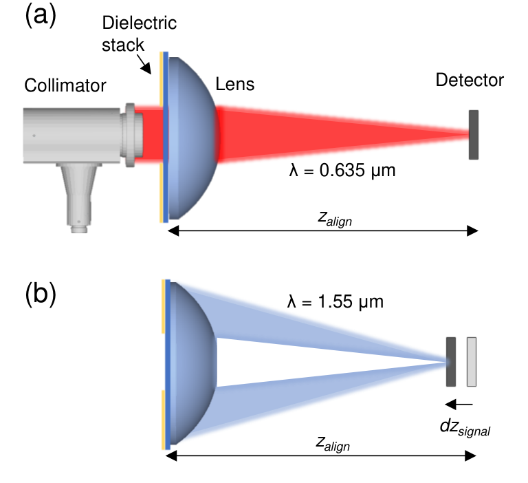

Ray tracing is used to calculate the estimated OCE for the system when it is aligned at this position, for the peak signal wavelength of 1700 nm (note this differs from the expected wavelength of 1550 nm due to larger-than-intended layer thicknesses). We identified two sources of misalignment that are sufficiently large to consider in this estimation, which are defocus (deviation from the best focal length in the z axis) and unwanted detector translation along the xy plane away from the calculated DM signal spot position. We estimate a defocusing uncertainty of 2.5 mm in our experiment. The translation error constitutes a fixed and known misalignment contribution as well as a systematic uncertainty. The fixed misalignment itself comes from (i) off-axis tilt in the reflective collimator, causing the alignment beam position to differ from the DM signal position by a small amount, and (ii) an initial error in the detector position when it was glued down, due to shifting during the curing of the epoxy used to fix it in place. Both these values were summed and used in the ray tracing simulations shown in Supplementary Fig. 6 as a starting location for the DM signal beam’s position relative to the detector. We noted that the alignment beam’s position in the plane of the detector was observed to vary by 100 m when inspected between cooldown cycles. As there is no reason for this error to vary during data collection once the apparatus has cooled to 300 mK, and since we cannot inspect the alignment beam’s position when cooled down, we incorporated this as a systematic uncertainty to be tested for worst-case estimation of the OCE. Ray tracing simulations were performed to compare several plausible misalignment scenarios. We varied the beam position by 100 m in either in-plane axis and by 2.5 mm along the focal length and found the worst case scenario of possible misalignment outcomes, in which the detector is shifted relative to the signal beam by +100 m along the x-axis, and -2.5 mm on the z-axis sending much of the beam off the surface at its most tightly focused point (Supplementary Fig. 6(a)). The OCE for this scenario is calculated to be 1.27%. In Supplementary Fig. 6(b) we also considered the best-case misalignment outcome, which gives an OCE of up to 7.2%. We note that displacement in the y-axis does not significantly affect any of the results, within the tolerance observed. rays were used for non-sequential ray-tracing. To simulate the effect of the DM signal’s angular spread (due to DM velocity dispersion), the rays were scattered with a Gaussian angular distribution (standard deviation of 0.85 mRad angular deflection per ray away from the normal vector). The lens was coated in simulations with the exact AR-coating that was applied to the real lens in the experiment. As a final note, we neglected the influence of signal light transmitted through the aperture portion of the stack, where the reflector is absent, as it is expected to be weak in comparison to the rest.
We also note the ray tracing results for a modified haloscope optical path (Supplementary Fig. 6(c)) which uses a plano-convex lens of a much larger focal distance (200 mm) with the convex side facing the stack. These changes would minimize the effects of spherical aberration and total internal reflection losses, resulting in a significantly improved OCE of 93%.
Earlier, we mentioned an anti-reflection (AR) coating applied to the lens in the haloscope. In our case, the coating is proprietary to the manufacturer of the lens and designed for broadband operation transmission within a certain spectral window (like the near-infrared, in our case), or a so-called broad-band anti reflection (BBAR) coating. Such a coating may consist of numerous alternating dielectric layers, typically arranged in a numerically optimized, aperiodic set of thicknesses. Since the number of layers and their composition are unknown to us, one may consider whether the BBAR coating could generate its own signal capable of destructively interfering with the dielectric stack’s own signal. In order for this to occur, several conditions must be satisfied: (1) the BBAR coating must be very specifically designed to concentrate a similar amount of power into the exact spectral window in which we are operating, (2) it must be almost perfectly co-planar across most of its surface, and specifically positioned to produce destructive interference, and (3) the dielectric stack and the BBAR coating must be less than a coherence length apart, in order for the signal powers to interfere at all. As discussed earlier in this Supplement, (2) is not satisfied, since wafer bow causes the gap between the stack and the lens to be significantly non-uniform, which would result in averaging of the signals over a large area, rather than perfect destructive or constructive interference. Additionally, small and slow thickness variation across the stack wafer introduces another effectively random perturbation to this distance. Moreover, (3) is not satisfied since the dielectric stack is at least one coherence length () away from the BBAR coating on the lens, considering the thickness of the stack substrate (525 m), plus contributions from the gap between the lens/stack from the epoxy used to attach them, and the additional gap due to wafer bow. Finally, we conducted ray tracing to consider a final aspect relevant to this issue: due to the wafer bow, a ray originating from a specific point on the BBAR coating and another ray originating from the same relative location on the dielectric stack are consistently displaced from one another along the focal plane of the detector (due to the effective local tilt of the stack wafer adding a defocus term to the BBAR coating’s signal). As a result, the two signals would be significantly misaligned on the detector, again preventing perfectly uniform interference. Since multiple conditions for uniform destructive interference from the BBAR coating are not satisfied, we conclude that it can be safely neglected from our experiment. However, in the future, it is worth considering that a deliberately designed and deposited BBAR coating on the lens could be an economical means of obtaining a thick and highly uniform dielectric stack in itself, without the need for a separate stack wafer.
We also conducted optical simulations of the SNSPD’s detection efficiency under various conditions for the purpose of validating our alignment strategy and confirming nominal operation of the SNSPD. We conducted a combination of 2D finite-element modeling and rigorous coupled-wave analysis Moharam and Gaylord 1981 to obtain this value, using the best available measurements of material thicknesses, refractive indices, and lateral dimensions of the as-fabricated SNSPD. Considering only the light incident from the top surface of the SNSPD, the theoretical detection efficiency is 32.7% for the parallel polarization (and 10.2% for the perpendicular polarization). However, given the large detection area of this device and the size of the near-infrared beam used for alignment, the reflection off the backside of the silicon substrate cannot be neglected in the calculation of the total absorption coefficient in the detector. This factor is most significant when the beam is centered on the detector area but focused on the bottom surface of the substrate. Conservatively, if we assume the worst case in which the focal spot of the beam is centered on the detection area and focused on the bottom side of the substrate, the light transmitted through the SNSPD will diffusely scatter off the unpolished back silicon surface with a Lambertian intensity profile. The total absorption coefficient of this backward pass can then be calculated by integration of light scattered to angles encompassing the SNSPD’s active area, and multiplication by the angle-dependent absorption coefficient of the SNSPD for light incident from underneath, referred to as the backward pass. For simplicity, we neglect light scattered into the perpendicular polarization, which has a much smaller absorption coefficient. Light scattered under a Lambertian profile has a radiant intensity proportional to the cosine of the angle between the incident beam and the surface normal Pedrotti et al. 2017. We start with the calculation of radiant flux emitted from a Lambertian surface wik:
where is the angle of incidence, and are the angular span of integration, and is is the peak radiant intensity chosen as so that when integrating from 0 to , the full angular range available in reflection. To calculate the angular dependence of the total absorption in the detector during the backward pass, we include the angular dependence of the detector’s absorption coefficient in the integral of the previous expression, and integrate over the angles of incidence in which the detector is visible to the point of reflection:
where is the total absorption coefficient of the backward pass, is the angle-dependent absorption coefficient of the detector from backward incidence (around 21% for relevant angles, obtained from 2D simulations), and is the maximum angle of incidence where the detector area is still visible to the reflected beam (0.49 rad). We calculate to be 4.9%. Next, we consider that only some of the original light incident on the top surface remains at the point of reflection off the back surface. The transmission coefficient through the detector, , is 0.62, and the reflection coefficient off the back surface is estimated to be uniformly 0.306, which when multiplied together and with result in an effective increase in the DE of about 1% due to the backward pass. Adding this to the forward-pass DE, the total detection efficiency of the SNSPD is estimated to be 33.6% in the case of an incident beam perfectly aligned to the detector area, and polarized parallel to the nanowire’s long axis. For the case of the perpendicular polarization, the backward pass has a marginal influence, increasing the total DE from 10.2% to about 10.6%. We ignore the effect of light scattered into the rest of the substrate, since the 1 cm2 die is large enough that most of the captured light will escape before encountering the relatively small detector area again.

Appendix C Dielectric stack fabrication and characterization
The dielectric stack, which is responsible for resonant conversion of DM particles to signal photons, was fabricated at NIST Boulder. The starting substrate was a fused silica wafer 50 mm in diameter, which was mounted with wax to a 150 mm-diameter carrier wafer at the position of best uniformity previously recorded for the deposition system to be used. Prior to film coating, it was plasma-cleaned in oxygen. The dielectric stack was deposited with alternating films of hydrogenated amorphous silicon (a-Si) and silicon dioxide (SiO2) deposited at 40°C with inductively-coupled plasma chemical vapor deposition (ICP-CVD). Based on measured deposition rates and prism-coupled refractive index measurements, the stack was designed to consist of 5 pairs of 292 nm a-Si and 548 nm SiO2. A gold reflector with a 5 nm Ti adhesion layer was deposited on top of the last SiO2 layer with electron beam evaporation.
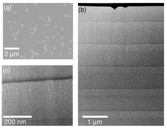

Supplementary Fig. 8 shows several images acquired through scanning transmission electron microscopy (STEM) and scanning electron microscopy (SEM) of one sample of the fabricated stack. Supplementary Fig. 8(a) is a top-view image showing the presence of numerous small (0.1 m2 area) pits present on the sample. These do not typically extend down to the bottom layer (as seen in Fig. 8(b)), but nevertheless we assume that no signal is generated from the area of the stack intersecting with any blisters, resulting in a stack transmission coefficient of 0.88 (or 12% loss) which factors into the final SDE calculation. Small interface effects were also observed between layers, which may be a consequence of sputtering damage or interdiffusion during the early stages of each layer’s deposition.
The precise layer thicknesses were determined with variable-angle spectroscopic ellipsometry over a wavelength range from 200 - 1700 nm. The refractive index of each type of film (such as a-Si or SiO2) was fitted over all measured data but assumed to be constant for all layers. Layer thicknesses were left uncoupled to allow for interlayer thickness variability. Experimentally, we observed actual thicknesses of 590 nm, 591 nm, 593 nm, 591 nm, and 595 nm for the SiO2 layers (starting at the gold reflector and moving toward the substrate), and 289 nm, 282 nm, 286 nm, 280 nm, and 288 nm for the a-Si layers in the same order. Considering two samples from different areas on the wafer, a variability of 0.2% was observed, which has a negligible effect on the stack’s behavior. The overall bias toward thicker-than-intended SiO2 layers may have resulted from different deposition behavior for the fused silica wafer which was wax-mounted to a silicon carrier wafer. The near-infrared refractive index of the a-Si layer was determined to be 2.64, and the refractive index of the SiO2 layer was 1.48, both measured at room temperature. Both indices are constant over the mirror’s spectral response range. The imaginary components of the refractive indices were previously measured to be in the wavelength range of interest to this experiment, making them negligible for the optical performance of the stack. While the optical properties of the stack are well known at room temperature, the a-Si may encounter some degree of thermo-optic shift during cooling to the 300 mK base temperature. We used the temperature dependence of the thermo-optic coefficient for crystalline silicon as a model Komma et al. 2012 and determined that the a-Si would drop to a refractive index of 2.61 (and the SiO2 would shift by a negligible amount). This has been factored into calculations for signal power generated by the stack.
We also characterized the properties of the stack’s substrate, which is a 50 mm diameter fused silica wafer with a nominal thickness of . In the context of this experiment, we are interested to know the surface topography and thickness variation of the wafers. Since DM has a coherence length of , and so signal photon generation is coherent over this length, it is important that the signal wavefront is not disturbed by a large amount over this span. Since the original stack wafer was destructively tested for precision measurements of the stack earlier, we analyzed several substrates from the same batch to capture the worst-case topography variations that could be expected. The wafers were scanned in two ways. The first way uses an array of mm size laser beams reflected off the surface and imaged at a distance to precisely measure wafer curvature and topographical variations over large areas. For a given wafer, it was scanned in a line across one axis, then was flipped upside down, and the scan repeated on the bottom surface in the same axis. The height variation in each case was taken relative to the middle of the wafer. This provides information on the relative variation of the substrate surfaces across its area. The top surface height variation is plotted in Fig. 10. The height is seen to vary by about 7 m across the entire surface, which is several times smaller than the magnitude of surface height deformation induced by wafer bow from intrinsic film stress. At its steepest slope, this is less than 0.2 m deviation per coherence length, which is a negligible amount. It is worth noting that no leveling is done on this height data, so we also plotted the difference between the top and bottom surface height variation as the red line in Fig. 10, showing little difference in the magnitude of the deviation.
To be certain that there were no high-spatial-frequency variations in surface topography, we also conducted 3D laser confocal scans of the surface in an area roughly as large as the coherence length. The relative surface height deviations were considerably smaller than the signal wavelength over the entire region, for several random regions measured on a given wafer. Thus, we conclude that the stack substrate surface height uniformity is sufficiently good for this experiment’s needs.
Taking all of these measurements in account, we obtained a conservative lower bound on the converted power, displayed in Fig. 3 of the main text, by minimizing the signal power over plausible values for the different target parameters. Specifically, we scanned the layer thickness over a range around their measured values, and the substrate thickness over a range around its nominal value. The refractive indices for the SiO2 layers were scanned over a range, while those for the Si layers were scanned over .

Appendix D SNSPD fabrication and testing
The device was fabricated from 7-nm thick WSi film which was sputtered on a 150 nm thick thermal silicon oxide film on a silicon substrate at room temperature with RF co-sputtering. Additionally, a thin 2-nm Si layer was deposited on top of the WSi film in-situ to prevent oxidation of the superconductor. To pattern the nanowires, electron-beam lithography was used with high-resolution positive e-beam resist. The ZEP 520 A resist was spin coated onto the chip at 5000 rpm which ensured a thickness of 335 nm. After exposure, the resist was developed by submerging the chip in O-xylene for 80 s with subsequent rinsing in 2-propanol. The ZEP 520 A pattern was then transferred to the WSi by reactive ion etching in CF4 at 50 W for 5 minutes. The ZEP thickness is estimated to be 250 nm after etching and is left on the top surface.
Supplementary Fig. 7 is a scanning electron micrograph (SEM) of the tungsten silicide (WSi) SNSPD after fabrication. The device area was 400 by 400 m2, and the nanowire was connected to external circuitry via two contact pads. The width of the nanowires was 140 nm with a pitch of 340 nm.
The switching current of the detector was 5.5 A measured at 300 mK by sweeping the current from a impedance source. Supplementary Fig. 12 shows the dependence of the count rate on the absolute bias current for 400 by 400 m2 large-area SNSPD at 1550 nm wavelength (0.8 eV). When the detector was illuminated, the count rate (open red dots) rose at a bias current of 3 A. Counts initially grew with the current and the device was nearly saturated at a bias current of 4.2 A. At this bias current, the count rate with the laser light turned off (background count rate) was below 100 counts/s. The maximum background count rate (black dots) was measured at a point just below the switching to the normal state, at counts/s. The open dots represent the background count rate when the fiber was decoupled from the haloscope. Blocking of infrared photons resulted in significant reduction of the background noise. With extrapolation of the experimental data, the expected count rate at the working bias current (vertical dashed blue line) for the long-duration integration experiment is Hz. However, deviations from this extrapolation are likely when going to very low bias currents, so direct measurements of dark counts at lower bias currents is desirable in the future.
Over the total 180 hour exposure, the experiment’s reference SNSPD registered 5 counts, while the haloscope detector registered 4 counts, with the latter corresponding to a count rate of . These counts were spread fairly evenly across the integration time, as illustrated in Supplementary Fig. 13. As discussed in the main text, we cannot be certain as to the cause of these events — plausible explanations include cosmic ray muons, Cherenkov photons generated in dielectric materials such as the lens, or current fluctuations in the detector. In particular, we do not necessarily expect the extrapolations for the intrinsic dark count rate, discussed above and shown in Supplementary Fig. 11, to hold down to the bias currents used during the exposure. Consequently, it is not surprising that the observed dark count rates are somewhat lower than the estimates from the previous paragraph.
Since the most plausible dark count mechanisms would result in almost the same dark count rates in the reference and primary SNSPDs, it is sensible to set limits on the signal rate (and correspondingly the kinetic mixing parameter ) assuming a common dark count rate. Specifically, we model the reference and primary counts as being independent and Poisson-distributed, with means and respectively, where is the expected number of dark counts and is the expected number of DM signal counts (for a given ). We view as an unknown parameter (since we do not have a precise estimate of the dark count rate), and derive a 90% limit on via requiring that
| (4) |
where are the reference and primary counts, and is the probability of observing counts given rates and . Since, if , we have for , the probability of obtaining a limit smaller than the true value is for any value of (where we take the limit to be sufficiently large if we observe ). Numerically, the LHS of Eq. (4) is maximized at , giving . We use this to derive the limit on displayed in Fig. 4 of the main text.

Appendix E Dark photon polarization
Our limits on the coupling of dark photon dark matter are derived under the assumption that the dark photon polarization direction varies randomly over timescales longer than the DM coherence time. This is the behaviour expected from the simplest early-universe production mechanisms, such as production from inflationary fluctuations Graham et al. 2016. As discussed in Caputo et al. 2021, it may be the case that for some other production mechanisms, the dark photon polarization direction is almost constant, over the time and length scales probed by the experiment. In such scenarios, our time-averaged power could deviate by up to from its value in the randomly-varying case, depending on the polarization direction. In addition, the proper statistical treatment of the noise will be slightly different, due to the time dependence of the signal photon rate. However, these effects make only a fractionally small () difference to our limits, so we do not display separate curves.
References
- Rubin and Ford (1970) V. C. Rubin and W. K. Ford, Jr., Astrophys. J. 159, 379 (1970).
- Aghanim et al. (2020) N. Aghanim et al. (Planck), Astron. Astrophys. 641, A6 (2020), arXiv:1807.06209 [astro-ph.CO] .
- Dine and Fischler (1983) M. Dine and W. Fischler, Phys. Lett. B 120, 137 (1983).
- Abbott and Sikivie (1983) L. F. Abbott and P. Sikivie, Phys. Lett. B 120, 133 (1983).
- Preskill et al. (1983) J. Preskill, M. B. Wise, and F. Wilczek, Physics Letters B 120, 127 (1983).
- Arias et al. (2012) P. Arias, D. Cadamuro, M. Goodsell, J. Jaeckel, J. Redondo, and A. Ringwald, JCAP 1206, 013 (2012), arXiv:1201.5902 [hep-ph] .
- Graham et al. (2016) P. W. Graham, J. Mardon, and S. Rajendran, Phys. Rev. D 93, 103520 (2016).
- Svrcek and Witten (2006) P. Svrcek and E. Witten, JHEP 06, 051 (2006), arXiv:hep-th/0605206 .
- Arvanitaki et al. (2010) A. Arvanitaki, S. Dimopoulos, S. Dubovsky, N. Kaloper, and J. March-Russell, Phys. Rev. D 81, 123530 (2010), arXiv:0905.4720 [hep-th] .
- Holdom (1986) B. Holdom, Phys. Lett. B166, 196 (1986).
- Cicoli et al. (2011) M. Cicoli, M. Goodsell, J. Jaeckel, and A. Ringwald, JHEP 07, 114 (2011), arXiv:1103.3705 [hep-th] .
- Dimopoulos and Giudice (1996) S. Dimopoulos and G. F. Giudice, Phys. Lett. B379, 105 (1996), arXiv:hep-ph/9602350 [hep-ph] .
- Damour and Polyakov (1994) T. Damour and A. M. Polyakov, Nucl. Phys. B423, 532 (1994), arXiv:hep-th/9401069 [hep-th] .
- Akrami et al. (2020) Y. Akrami et al. (Planck), Astron. Astrophys. 641, A10 (2020), arXiv:1807.06211 [astro-ph.CO] .
- Baryakhtar et al. (2018a) M. Baryakhtar, J. Huang, and R. Lasenby, Phys. Rev. D 98, 035006 (2018a).
- Arvanitaki et al. (2018) A. Arvanitaki, S. Dimopoulos, and K. Van Tilburg, Phys. Rev. X 8, 041001 (2018).
- Goodman and Witten (1985) M. W. Goodman and E. Witten, Phys. Rev. D 31, 3059 (1985).
- Caldwell et al. (2017) A. Caldwell, G. Dvali, B. Majorovits, A. Millar, G. Raffelt, J. Redondo, O. Reimann, F. Simon, and F. Steffen (MADMAX Working Group), Phys. Rev. Lett. 118, 091801 (2017), arXiv:1611.05865 [physics.ins-det] .
- Carosi et al. (2020) G. Carosi, R. Cervantes, S. Kimes, P. Mohapatra, R. Ottens, and G. Rybka, in Microwave Cavities and Detectors for Axion Research, edited by G. Carosi and G. Rybka (Springer International Publishing, Cham, 2020) pp. 169–175.
- Phillips (2017) B. Phillips, in 2nd Workshop on Microwave Cavities and Detectors for Axion Research, Lawrence Livermore National Laboratory (2017).
- Sloan (2015) J. Sloan, in 1nd Workshop on Microwave Cavity Design for Axion detection, Livermore Valley Open Campus (2015).
- Baryakhtar et al. (2018b) M. Baryakhtar, J. Huang, and R. Lasenby, Phys. Rev. D98, 035006 (2018b), arXiv:1803.11455 [hep-ph] .
- Hochberg et al. (2019) Y. Hochberg, I. Charaev, S.-W. Nam, V. Verma, M. Colangelo, and K. K. Berggren, Phys. Rev. Lett. 123, 151802 (2019).
- Reddy et al. (2020) D. V. Reddy, R. R. Nerem, S. W. Nam, R. P. Mirin, and V. B. Verma, Optica 7, 1649 (2020).
- Verma et al. (2020) V. B. Verma et al., “Single-photon detection in the mid-infrared up to 10 micron wavelength using tungsten silicide superconducting nanowire detectors,” (2020), arXiv:2012.09979 [physics.ins-det] .
- Wollman et al. (2017) E. E. Wollman et al., Opt. Express 25, 26792 (2017).
- Du et al. (2020) P. Du, D. Egana-Ugrinovic, R. Essig, and M. Sholapurkar, “Sources of low-energy events in low-threshold dark matter detectors,” (2020), arXiv:2011.13939 [hep-ph] .
- Andrianavalomahefa et al. (2020) A. Andrianavalomahefa et al. (The FUNK Experiment), Phys. Rev. D 102, 042001 (2020).
- Barak et al. (2020) L. Barak et al. (SENSEI Collaboration), Phys. Rev. Lett. 125, 171802 (2020).
- Angle et al. (2011) J. Angle et al. (XENON10 Collaboration), Phys. Rev. Lett. 107, 051301 (2011).
- An et al. (2020) H. An, M. Pospelov, J. Pradler, and A. Ritz, Phys. Rev. D 102, 115022 (2020).
- McCabe (2010) C. McCabe, Physical Review D 82 (2010), 10.1103/physrevd.82.023530.
- Millar et al. (2017) A. J. Millar, G. G. Raffelt, J. Redondo, and F. D. Steffen, JCAP 01, 061 (2017), arXiv:1612.07057 [hep-ph] .
- Horns et al. (2013) D. Horns, J. Jaeckel, A. Lindner, A. Lobanov, J. Redondo, and A. Ringwald, JCAP 1304, 016 (2013), arXiv:1212.2970 [hep-ph] .
- Suzuki et al. (2015) J. Suzuki, T. Horie, Y. Inoue, and M. Minowa, JCAP 1509, 042 (2015), arXiv:1504.00118 [hep-ex] .
- Marsili et al. (2012) F. Marsili, F. Bellei, F. Najafi, A. E. Dane, E. A. Dauler, R. J. Molnar, and K. K. Berggren, Nano letters 12, 4799 (2012).
- Weinberg (1978) S. Weinberg, Phys.Rev.Lett. 40, 223 (1978).
- Wilczek (1978) F. Wilczek, Phys.Rev.Lett. 40, 279 (1978).
- Peccei and Quinn (1977) R. Peccei and H. R. Quinn, Phys.Rev.Lett. 38, 1440 (1977).
- Graham et al. (2015) P. W. Graham, I. G. Irastorza, S. K. Lamoreaux, A. Lindner, and K. A. van Bibber, Annual Review of Nuclear and Particle Science 65, 485 (2015).
- Polakovic et al. (2020) T. Polakovic, W. Armstrong, V. Yefremenko, J. Pearson, K. Hafidi, G. Karapetrov, Z.-E. Meziani, and V. Novosad, Nuclear Instruments and Methods in Physics Research Section A: Accelerators, Spectrometers, Detectors and Associated Equipment 959, 163543 (2020).
- Lawrie et al. (2021) B. J. Lawrie, C. E. Marvinney, Y.-Y. Pai, M. A. Feldman, J. Zhang, A. J. Miller, C. Hua, E. Dumitrescu, and G. B. Halász, “Multifunctional superconducting nanowire quantum sensors,” (2021), arXiv:2103.09896 [quant-ph] .
- Moharam and Gaylord (1981) M. G. Moharam and T. K. Gaylord, J. Opt. Soc. Am. 71, 811 (1981).
- Pedrotti et al. (2017) F. L. Pedrotti, L. M. Pedrotti, and L. S. Pedrotti, Introduction to optics (Cambridge University Press, 2017).
- Lyon et al. (1977) K. G. Lyon, G. L. Salinger, C. A. Swenson, and G. K. White, Journal of Applied Physics 48, 865 (1977), https://doi.org/10.1063/1.323747 .
- Hahn and Kirby (1972) T. A. Hahn and R. K. Kirby, AIP Conference Proceedings 3, 13 (1972), https://aip.scitation.org/doi/pdf/10.1063/1.2948551 .
- (47) “Thin film mechanics,” https://www.mrsec.harvard.edu/education/ap298r2004/Vlassak%20AP298presentation.pdf.
- Stoney and Parsons (1909) G. G. Stoney and C. A. Parsons, Proceedings of the Royal Society of London. Series A, Containing Papers of a Mathematical and Physical Character 82, 172 (1909).
- (49) “Lambert’s cosine law,” https://en.wikipedia.org/wiki/Lambert’s_cosine_law.
- Komma et al. (2012) J. Komma, C. Schwarz, G. Hofmann, D. Heinert, and R. Nawrodt, Applied Physics Letters 101, 041905 (2012), https://doi.org/10.1063/1.4738989 .
- Caputo et al. (2021) A. Caputo, A. J. Millar, C. A. J. O’Hare, and E. Vitagliano, (2021), arXiv:2105.04565 [hep-ph] .
- (52) See Supplemental Material for additional experimental and theoretical details, which includes Refs. [43-51].