Scaling Up Silicon Photonic-based Accelerators:
Challenges and OpportunitiesPreprint: AIP/123-QED
Abstract
Digital accelerators in the latest generation of CMOS processes support multiply and accumulate (MAC) operations at energy efficiencies spanning 10-to-100 fJ/Op. But the operating speed for such MAC operations are often limited to a few hundreds of MHz. Optical or optoelectronic MAC operations on today’s SOI-based silicon photonic integrated circuit platforms can be realized at a speed of tens of GHz, leading to much lower latency and higher throughput. In this paper, we study the energy efficiency of integrated silicon photonic MAC circuits based on Mach-Zehnder modulators and microring resonators. We describe the bounds on energy efficiency and scaling limits for optical networks with today’s technology, based on the optical and electrical link budget. We also describe research directions that can overcome the current limitations.
I Introduction:
Vector matrix multiplication operations represents the core of artificial neural networks (ANNs) and other computing applications of hardware accelerators. ANNs are realized in digital complementary metal–oxide-semiconductor (CMOS) circuits with multiple processing elements implementing multiply and accumulate (MAC) operations which calculates the product of two numbers and adds the result to an accumulator Sze et al. 2017. The processing elements can be arranged in a systolic architecture, where data is passed through connected processing elements in a rhythmic sequence, to perform MACs either spatially or temporally over several clock cycles Kung 1982.
Integrated silicon photonics (SiP) circuits have been popularly employed in high-speed links to move data at a rate of tens of Gb/s, where optical modulation is more efficient than electronic switching for transmitting data over significant distances Ahmed et al. 2020. Optical modulation can be realized using Mach Zehnder modulators (MZMs) or microring modulators (MRMs) Ahmed et al. 2016. MZMs are broadband and easily support complex modulation schemes Ahmed et al. 2020. MRMs have significantly smaller footprint and driver power consumption Moazeni et al. 2017. As a technology, the current generation of SiP has now matured with high volume shipments for datacenter transceivers from companies such as Intel and Cisco. SiP circuits comprising of Mach Zehnder interferometers (MZIs) or microring resonators (MRRs) have been used also for other applications such as high-speed optical switches and filters AlTaha et al. 2019; Jayatilleka et al. 2019; Dong, Melikyan, and Kim 2018; Ikeda et al. 2020; Bhaskar et al. 2020.
SiP is also being used for computing applications Tait et al. 2019; Shen et al. 2017; Hughes et al. 2018; Bangari et al. 2019; Shekhar 2021; Ramey 2020, where devices such as MZIs, MZMs, MRRs, and MRMs are used for computation in optical analog domain. These encompass inference and training accelerators used for machine learning and neuromorphic computing applications where convolution takes of the total processing time Li et al. 2016a; Huang et al. 2022; Filipovich et al. 2021. Other integrated optical configurations implemented using field-programmable photonic arrays were shown to carry out linear transformations for signal processing and control Pérez, Gasulla, and Capmany 2018; Zhang and Yao 2020. Linear transformation circuits are also employed in Ising machinesTezak et al. 2020 and photonic quantum computing processors Qiang et al. 2018.
In this Perspective, we describe the advantages and challenges of implementing MACs using SiP, and comment on how to address them. The paper is organized as follows: Section II and III describe the link budget, energy efficiency and scaling opportunities for SiP MACs implemented with MZM and MRM, respectively. Section IV explores the possible approaches to further improve SiP MAC systems. It introduces the ongoing research in the field of SiP that when fully realized, will lead to significant changes in the field of optical computing and communication. Section V concludes the paper.
II MZM Based Si-photonic Implementation
II.1 System Architecture
Fig. 1 illustrates an MZM-based SiP implementation of an optical accelerator. Using off-chip lasers, light is guided by a polarization-maintaining (PM) single mode fiber (SMF), gets coupled to the SiP chip via an edge coupler and then split to parts. These parts are modulated by an array of MZI modulators and fed into an weight transformation (multiplication) matrix, . The optical intensities at the MAC outputs, , are thus described by the multiplication product of the input vector, and the weight matrix, , as:
| (1) |
In other words, the weight matrix performs linear transformation for the input vector, , and delivers outputs, , that are routed to an array of photodetectors (PDs). These PDs are then connected to the electrical components, including TIAs, main amplifiers, and sense amplifiers based comparators, which are either built in a separate CMOS/BiCMOS chip, or monolithically integrated with the SiP devices in the same process.
Singular value decomposition (SVD) is an effective approach to represent a given matrix as a factorization of multiple matrices Lawson and Hanson 1995; Golub and Reinsch 1970. SVD decomposes a real matrix into a product of unitary matrices and a diagonal matrix. This is useful in the experimental realization of an matrix topology in which the sequential product of rotation matrices represents the sequential arrangement of linear transformation units in the overall matrix grid Reck et al. 1994. A linear transformation unit in the whole grid arrangement is practically implemented using a tunable beam splitter (TBS) as seen in Fig. 1 Clements et al. 2016; AlTaha et al. 2019. A TBS comprises of an MZI with a phase shifter () in at least one of the arms, along with either an outer phase shifter () or a tunable directional coupler Pai et al. 2019; Taballione et al. 2019. The transfer function for a single TBS can be described using the matrix representations for ideal 50:50 beam splitters and lossless phase shifters as:
| (2) | ||||
Thus, any arbitrary light redistribution can be obtained by changing and .
The SVD decomposition of the weight matrix can be described as:
| (3) |
where is a diagonal matrix, and represents the transformation matrix for a node between two input terminals, and , within the multiplication matrix Clements et al. 2016, given as:
| (4) |
II.2 Optical Network Link Budget
The photonic components shown in Fig. 1 are simulated in Cadence Spectre for and transformation matrix sizes to verify the optical link budget analysis. The optical components are modeled in Verilog-A to enable electronics-photonics co-simulation Shekhar et al. 2016; Sorace-Agaskar et al. 2015. The models of some of the components used in this paper are derived from Sorace-Agaskar et al. 2015, with some modifications to account for the laser electrical power consumption, the wall plug efficiency, , link losses, etc. The optical power of laser is set to 0 dBm to estimate the optical power at the output terminals of the network, incident on the PDs. Coupling light to the SiP chip introduces loss in the range of 0.6-to-3 dB based on the coupling scheme used Dietrich et al. 2018; Honmou et al. 1986. The overall coupling loss from the laser to the SiP chip is collectively estimated as 1.6 dB considering possible optimizations in the coupling efficiency. 1.6 dB is also a realistic estimate for photonic wire bonds (PWBs), an emerging technology which involves writing three-dimensional waveguides in a photosensitive polymer. PWBs have demonstrated efficient interfacing between the external sources to the silicon waveguide with coupling losses as low as 0.4 dB up to 1.7 dB Won 2018; van; Billah et al. 2017; Lindenmann et al. 2012; Lindenmann et al. 2015.
For an input vector size of , light passes through splitters before modulation, resulting in a total insertion loss of dB, where is the estimated excess loss for a single splitter and ranges between 0.01 dB to 0.5 dB Chrostowski et al. 2019; Li 1997; Samani et al. 2016; Dai, Ma, and Wu 2017; González-Andrade et al. 2019. The estimated excess loss for beam splitters and combiners in this study is 0.01 dB. The overall attenuation in the silicon waveguide is a function of the depth of the network. The MZM based implementation is based on Clement’s arrangement which is composed of beam splitters and phase shifters that can be programmed to implement linear transformationClements et al. 2016. With an MZM representing one node in Clements arrangementClements et al. 2016, the waveguide attenuation can be approximated as , where represents the optical intensity attenuation in the Si waveguide and is the length of an MZM arm, with chosen values of 3 dB/cm and 0.5 mm respectively. The insertion loss introduced by an MZM’s PN phase shifter is approximated as 1 dB/mm Samani et al. 2016.
The insertion loss through a node is dependent on the excess loss for cross and through states, and , respectively, both of which are typically 1 dB Lu et al. 2015; Chen et al. 2016. For simplicity, two phase shifters connected by 3 dB adiabatic directional couplers ( 0.1 dB)Chrostowski et al. 2019 are assumed in this work for analysis.
To study the optical attenuation of the MZM implementation shown in Fig. 1 and verify its functionality, all inputs, except for the uppermost terminal (), are driven by voltage that creates a phase shift difference between their MZM’s arms and null their outputs. As light is set to propagate through the uppermost input terminal, the optical depth is defined by the route passing through the diagonal TBS nodes with .
For a rectangular mesh arrangement, the matrix optical depth is equal to with a total number of optical crossings Clements et al. 2016; Reck et al. 1994. Hence, the matrix implementation shown in Fig. 1, has an optical depth of 8 with 28 crossings.
The total optical link budgets are calculated based on (5), where , , , , , and represent the attenuation introduced by the SMF fiber, fiber to chip coupling loss, silicon waveguide attenuation, splitter insertion and excess loss, phase shifters’ insertion loss, total adiabatic coupling insertion loss and network penalty, respectively. The network penalty takes into account further impairments due to extinction ratio, cross talk, intersymbol interference (ISI) and laser relative intensity noise (RIN) which is caused by the random spontaneous emission over time Ahmed et al. 2016; Hui 2020; Li et al. 2016b.
| (5) | ||||
Fig. 2 shows the calculated optical power throughout networks with different inputs vector sizes. The optical power of the laser is set to for ease of illustration. Besides the attenuation due to the splitting, it can be noticed that the losses introduced by the optical components in the multiplication matrix (i.e. directional couplers and phase shifters) pose a limitation for scaling the network due to the highly attenuated optical intensities reaching the outputs. Fig. 3 shows the optical intensities required at the analog front-end (AFE) to detect a signal with a resolution of bit. This is obtained by representing the desired output signal and current noises in terms of the received optical intensity as given in Eq. (8). The blue dotted lines represent the optical power at the matrix outputs and the corresponding bit resolution for a laser intensity of . It can be shown that the maximum achievable matrix size is for binary networks operating at . We revisit this calculation again in Section II.4.
II.3 Energy Efficiency
The total electrical power dissipation of the whole network comprises of the power consumed by the laser, input modulators, thermo-optic tuning of the matrix phase-shifters, and the AFE including PDs. Accordingly, for a configuration of size operating at a data rate of , the energy efficiency (J/Op) can be calculated as:
| (6) | ||||
where , , , and represent the electrical power dissipated due to the laser, input modulator drivers, data fetch interfacing circuits, matrix tuning and the output AFE circuits, respectively. represent the electrical power dissipated if a semiconductor optical amplifier (SOA) is used to recover the loss.
The factor refers to the energy efficiency enhancement. It can be represented as where represents the energy scaling due to the loss of precision factor, and will be described later in Section II.4. represents the efficiency enhancement due to an SOA. Assuming an SOA introducing a gain of (in dB), the corresponding enhancement is . The use of an SOA is discussed later in Section IV, but it can be inferred from Eq. (6) that the use of an SOA always degrades the overall energy efficiency.
The amount of power dissipated by the laser is represented in terms of the laser’s wall plug efficiency, , the optical insertion losses introduced by the SMF fiber, , the fiber to chip coupling , the silicon waveguide loss, , the input MZM loss, , the weight phase shifter loss, , the directional coupler loss, , as well as the receiver’s PD sensitivity, , as given in Eq. (7).
| (7) | ||||
The total length of the waveguide was roughly approximated as the length spanning the optical depth of the matrix only. The output sensitivity is solved based on the targeted bit resolution, as well as the total noise at the output front-end due to the photodetector shot noise, dark current , thermal noise and laser relative intensity noise (RIN) as given in Eq. (8), with values reported in Table 1. The parameters , , and represent the PD responsivity, output load resistance, Boltzmann’s constant and the absolute temperature.
| (8) |
| Giewont et al. 2019 | ||
| Giewont et al. 2019 | ||
| Hui 2020; Li et al. 2016b | ||
The MZM drivers consume power that scales linearly with as , where represents the energy efficiency of the MZM driver. For binary resolution, the power consumed by the drivers and AFEs are extracted from recent work on PAM2, and is typically in the range of 2pJ/b Szilagyi et al. 2018.
The matrix weights are tuned using thermo-optic phase shifters (TO-PS). Doped Si heaters on SOI platform typically dissipate about 20 mW for a -shift AlTaha et al. 2019; Jacques et al. 2019; Harris et al. 2014. The efficiency of TO-PS can be improved using other heater materials such as TiN, substrate undercut to improve insulation and deep trenches to reduce thermal cross-talk Jacques et al. 2019; Nakamura et al. 2012. This can be shown to significantly improve the overall energy efficiency of the network as illustrated in Fig. 5. Assuming uniformly distributed weights, the expected energy consumption of the thermo-optic phase shifter is , where denotes the amount of electrical power required to create a phase shift of . Calculating for all the nodes in Clement’s topology, the total average tuning power is .
After optical processing, the optical data needs to be converted to the electrical domain to be processed, stored or reused in other networks. Efficient opto-electronic receivers, comprising of a PD, TIA and main amplifiers have been shown to have energy efficiencies pJ/b Liu et al. 2012; Lee and Chen 2018; Takemoto et al. 2010; Morita et al. 2014; Schow et al. 2009; Park et al. 2010. For an AFE operating at Gb/s and realized in CMOS technology, an energy efficiency of pJ/bLiu et al. 2012 is assumed for the calculation of binary resolution AFE, which scales with a factor of for the whole output array. Higher AFE resolutions entail the use of linear TIAs along with analog to digital converter (ADC) circuits to recover the digital data. High speed linear TIAs have shown efficiencies as low as pJ/b Lakshmikumar et al. 2019. The energy consumption for ADCs is extracted from the energy per conversion figure of merit (FOM) such that . The energy consumption values used in this work for , and are pJ/b, pJ/b and pJ/b based on a FOM of pJ/conversion for an ADC designed to operate at a sampling rate of GS/s Frans et al. 2017.
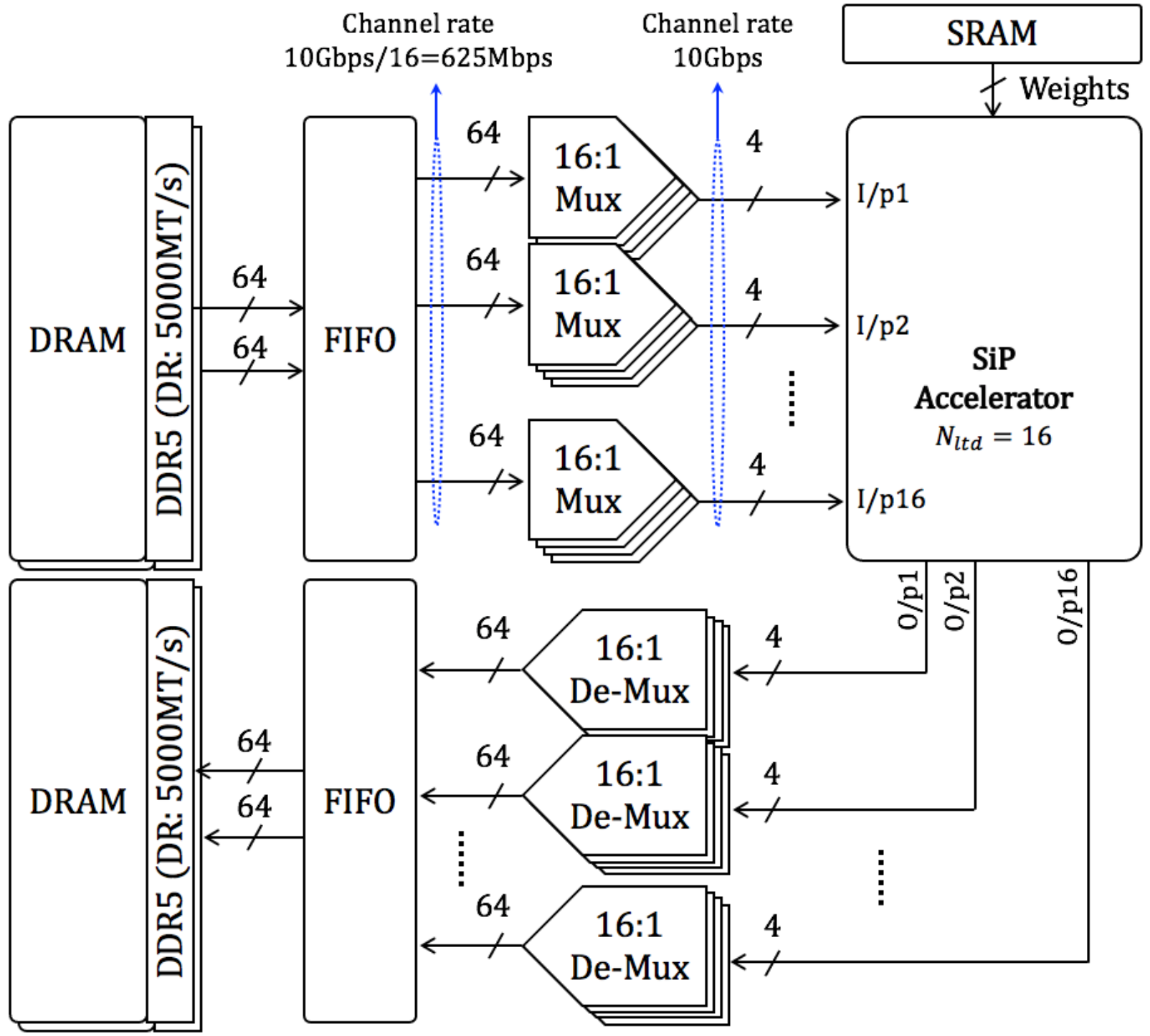
Providing high-speed serial inputs to the SiP accelerator requires FIFOs and multiplexers to interface the data transfer with DRAM, as shown in Fig. 4. For a fair comparison to digital CMOS implementations, the power dissipation for both input and output interfacing circuits, represented by is taken into consideration in the energy efficiency calculation of SiP implementations. The power dissipated by the FIFO, multiplexers, clock dividers and retimers is estimated as in CMOS based on the data reported in Cao et al. 2002 in CMOS technology.
II.4 Efficiency Tradeoff Factors
It can be inferred from Eq. (7) that the required input laser power increases as a function of as a result of the exponentially increasing optical losses in the MZM based accelerator. But the total energy efficiency Eq. (6) starts improving as scales up due to the quadratic increase in the number of accelerated operations performed by the optical matrix as shown in Fig. 5. Taking all optical losses into account shows that there is a scaling limit beyond which optical losses grow significantly and the overall efficiency drops and an optimal network size exists for minimum energy efficiency. Unfortunately, the maximum network scale, , is limited by the rated output optical power of the laser and the SNR required for any given signal resolution, , as given in Eq. (8) and illustrated in Fig. 3.
Fig. 6 shows the total energy efficiency and scaling limit for various input resolutions considering thermo-optic phase shifters with and without insulation. The energy efficiencies in Fig. 6 are calculated for accelerators to be operated at binary and higher resolution, . Although the probability of transition reduces for multilevel signaling Moazeni et al. 2017, the requirement on driver’s linearity or segmentation also increases. Furthermore, the energy consumed in the serializing and clocking remains the same Moazeni et al. 2017. Thus, we assume similar energy efficiency for multilevel signaling as PAM2, , for MZM modulatorsTanaka et al. 2018. For binary resolution, the power consumed by the drivers and AFEs are extracted from recent work on PAM2 transceiversTanaka et al. 2018; Moazeni et al. 2017; Michard et al. 2020; Lakshmikumar et al. 2019; Tanaka et al. 2018. Therefore, the energy efficiency for , and input MZM drivers are estimated in our calculation as , and per symbol, respectively.
It can be concluded from Fig. 6 that opting for PDs with higher responsivities improves the energy efficiency of the network. This compensates for the optical system loss, relaxes the need to inject high optical power at the network input and improves the overall energy efficiency. Utilizing avalanche PDs (APDs) is a possible way to significantly improve the optical sensitivity Nayak et al. 2019. Fig. 6 also suggests that taking advantage of the loss of precision, when possible, shows minor improvement in the energy efficiency and the network scaling.
Considering a matrix that scales with , the laser optical intensity should be typically scaled by a factor of to account for the splitting loss in a lossless network. For mesh-like configurations similar to Fig. 1, scaling the input vector size increases the dynamic range of the output intensities. In other words, for a given matrix output, the intensity can be as low as that of a single input or as high as times that amount. With the input’s digital resolution being , the effective overall output resolution due to the network scaling is .
The conservative estimate of scaling the input power by may not be necessary in some computational context such as convolutional neural network (CNN) layers with adaptable hidden layer resolutions Moons et al. 2016; the increased output resolution might be higher than that needed by the AFE to detect. Therefore, an energy scaling vs. loss of precision trade-off factor, , can be introduced to take advantage of the network scaling, Nahmias et al. 2020; Agarwal et al. 2016, as illustrated in Fig. 7. Full accuracy is described by corresponding to reduced output precision of , at which the input optical intensity is scaled by . Generally, for bit reduction, the input is scaled by . Therefore, the maximum amount of energy saving is achieved when the bit reduction is tolerable at the optical output (AFE input).
To get a meaningful sense of the trade-off between the energy scaling and the loss of precision, is quantified in Eq. (9) in terms of the probability of bit errors for binary networks (networks with binary weights) at the output such that:
| (9) |
where the function is defined as , and represents the total input referred noise at the AFE input with contributions from the PD, TIA, main amplifiers and comparators (if applicable). Therefore, the laser power, , can be traded off for loss of output resolution.
The IL difference between the bar and cross states of a tunable beam splitter impacts the interference between the nodes in the mesh. For an MZM with intensity loss of in one arm and in the other, it can be shown that the output intensity at the cross state is given by when , where and represent the MZM input intensities at its input ports 1 and 2, respectively. To get the transmission response of an MZM with equal losses, on both arms, should be modified such that in order to account for the loss difference between the two MZM arms, where and describes the phase shift when both arms have attenuation of . This difference in insertion losses can be observed in single-arm beam splitters in which phase shifters are controlled by a single arm only. Using dual-arm tunable beam splitters, where is implemented differentially using phase shifters on both arms, introduces equal insertion losses for the bar and cross transmissions of each node. A dummy phase shifter can also be used in single-arm topologies to obtain equal losses.
For sake of comparison, the energy consumption for a digital MAC is estimated based on the energy consumed by multiplication and accumulation operations as well as register file access in a CMOS implementation Gudaparthi et al. 2019. With an estimated energy consumption 0.046 pJ for 8b MAC and 0.0117 pJ for register file access, the calculated energy consumption is pJpJ=fJ for a single operation. Conversely, it can be observed from Fig. 6 that SiP networks based on MZMs need to be scaled down to achieve higher resolutions which further degrades their energy efficiency. Compared to their 8b digital CMOS counterpart, the energy efficiencies for SiP MZM MACs (using low-power thermo-optic phase shifters with insulation and 1.2 A/WBenedikovic et al. PD responsivity) at = 1b to 4b resolutions are to worse. Despite the lower energy efficiency, MZM-based MAC operations are performed at 2 higher operating speed and lower latency (for a weight-stationary systolic array with input vector size of ) than the corresponding digital CMOS implementation.
In addition, multiple clock cycles are needed for digital multipliers and adders to provide the MAC output in systolic arrays. Operating at lower clock speeds further decreases their throughput in comparison to optical implementations. Assuming a number of clock cycles needed for digital MAC, the latency of a digital systolic array with a input vector size and a matrix size is where represent the clock frequency of the digital CMOS implementation. Hence, the throughput ratio of the optical to CMOS implementations is , where represents the clock speed at which an optical implementation operates at.
We also investigate the energy efficiency and network size at lower data rates in Fig. 8. Intuitively, the energy efficiency degrades at lower data rates because less number of operations are conducted with respect to the dissipated static power. On the other hand, the network size, shown in Fig. 8, can be increased by making use of the SNR improvement at lower data rates, as inferred from Eq. (8). If maximizing the optical throughput is not an overarching goal, opting for lower data rates (relative to 10 GS/s) leads to larger networks while not sacrificing much on the energy efficiency in implementations incorporating phase shifters with insulation (which do not consume much static power as shown by the dotted curves in Fig. 8 (a)).
III MRR Based Si-photonic Implementation
III.1 System Architecture
The SiP MRR-based implementation of an optical accelerator is illustrated in Fig. 9. A comb CW laser source is used to provide wavelengths through which are coupled into the chip and then modulated by an array of MRMs. Unlike mesh-like topologies, implementing vector matrix multiplication in the form of dot products has the advantage of maintaining equal path loss for all the outputs. The modulated input vector, , is then split (broadcast) into branches to be modulated by the weight bank arrays Tait et al. 2014; each output represents the dot product of the input vector and one of the row arrays of the weight matrix. In order to achieve weights with positive and negative polarities, the thru and drop transmissions of the weight arrays are routed to balanced PDs in a push-pull configuration at the receiver. The current difference at the output, , can be represented as Bangari et al. 2019:
| (10) |
where , and represent the amplitude of the input optical field, the difference between the weight’s drop and thru intensity transmissions and the PD responsivity at a wavelength , respectively.
III.2 Optical Network Link Budget
Similar to Eq. (5), the optical link budget is calculated based on Eq. (11):
|
|
(11) |
where represents the transmission insertion loss of the MRM for the input vector, represents out of band insertion loss () of the MRM for the input vector when the MRM resonance wavelength does not match the input vector wavelength, represents transmission insertion loss of the MRR for the weight vector, and represents out of band insertion loss of the MRR for the weight vector. Other terms have been defined already when describing Eq. (5).
| Li et al. 2021 | |
Fig. 10 shows the calculated optical power throughout an MRR-based implementation with different input vector sizes, , using the values shown in Table 3. The optical power of the laser is set to for the ease of illustration. Similar to MZM-based implementations, the attenuation introduced due to the splitting and cascading of microrings significantly degrade the optical power and pose a limitation on the energy efficiency as will be discussed in Section III.3. Fig. 11 shows the optical intensities required at the AFE to detect a signal with a resolution of bit. This is obtained by representing the desired output signal and current noises in terms of the received optical intensity as given in Eq. (8). It can be shown that the maximum achievable matrix size is for binary networks. We revisit this calculation again in Section III.4.
III.3 Energy Efficiency
The energy efficiency of the MRM-based implementation with size operating at a data rate of can be calculated as:
| (12) | ||||
here represents the total electrical power consumed by the optical source (either a single comb laser source or multiple sources generating all the desired input wavelengths). To better study the energy efficiency based on a targeted signal resolution, , the power consumption of the input laser source is formulated as a function of the optical power reaching the PDs at the output AFE as given in (13).
| (13) | ||||
where represents the gap between the centers of two adjacent microrings and is dictated by the thermal crosstalk which should be taken for design considerations. A of has been shown to be sufficient to avoid thermal crosstalk in a photonic switch implementation Konoike et al. 2019. We assume a of in this work for an optimistic realization of the system with .
Since the number of operations scale quadratically with the weight vector size, , while the energy consumption of the modulators and AFE increases linearly as can be seen in (12), the overall energy efficiency improves with scaling as shown in Fig. 12. We assume similar MRM energy efficiency for multilevel signaling as PAM2, , Moazeni et al. 2017 which takes into account both the contribution of the modulator driver as well as the serializers. Therefore, the energy efficiency for , and input MRM drivers are estimated in our calculation as , and per symbol, respectively.
MRMs offer smaller footprint and lower input capacitance which leads to significant reduction in their driving power. However, they are also more sensitive to fabrication mismatch and thermal drift which entails the need to use heaters for calibration across a wide spectral range. Excluding heater power, the power consumed by a closed loop controller implemented for a low-power WDM topology is Zheng et al. 2014. The average energy efficiency for state-of-the-art MRR heaters on an SOI platform is Gan et al. 2007; Jayatilleka et al. 2019; Masood et al. 2013. The scaling of the power consumed by the heaters with degrades the overall energy efficiency of the network. Fig. 13 shows the total energy efficiency and scaling limit for various input resolutions considering thermo-optic phase shifters with and without insulation. We assume power consumption values, , of Masood et al. 2013 and Jayatilleka et al. 2019 for phase shifters with and without insulation, respectively, to provide phase shift of one free spectral range (FSR).
III.4 Scaling Limitations
It can be inferred from Fig. 13 that it is feasible to implement vector matrix multiplication using MRR based networks with sizes scaling up to . For or above, the network size is within the maximum number of microrings permitted for WDM implementations due to FSR limitations and crosstalk Tait et al. 2016. Attempting to engineer the MRR’s dimensions and coupling ratio compromises the quality factor which degrades the channel spacings. This translates to a limit in the MRR vector size of . Channel spacings are typically set according to the amount of acceptable crosstalk between channels (interchannel interference). As an example, for a transmission window with channel spacings of , the maximum number of channels is Jayatilleka et al. 2016; Tait et al. 2016. Thus, for , FSR may set a limitation to the overall network size.
Using series coupling to increase the filter order has been experimentally shown to reduce both interchannel and intrachannel crosstalks, thus, maximizing the filter finesse and the channel count Jayatilleka et al. 2016. However, this comes at the expense of higher footprint, lower drop port transmission and extra tuning power. To cascade several MRRs for MAC operations, it is necessary to maintain channel spacings to avoid the adjacent weight-dependent cross-talk. The number of channels that can be supported by optimized MRRs with finesse of 368 and 540 are calculated to be 108 and 148, respectively Tait et al. 2016; Xu, Fattal, and Beausoleil 2008; Biberman et al. 2012.
Two-point coupling scheme has been proposed to address the post-fabrication correction of MRM spectral features for large-scale MRM implementations Shoman et al. 2019. Although it mitigates the secondary resonances of an MRM and doubles the FSR, an extra micro-heater is introduced to correct for the coupling which increases the power consumption. Another attempt to achieve an FSR-free filter has been demonstrated using tunable couplers along with modified vernier filters that use higher-order coupled MRRs Milanizadeh et al. 2020. However, this topology is associated with penalty in terms of design complexity, increased footprint and tuning power.
Introducing contra-directional coupling (CDC) in a microring combines the wavelength selectivity of the CDC with the compact feature size of the MRR, thus reaping the advantages of both and providing an FSR-free response Eid et al. 2016. Implementing this design technique allows the potential use of several channels in MRR-based accelerators. This comes with a tradeoff of using extra heaters in the CDC and in the region of the MRR that does not include corrugated structures.
As shown in Fig. 13, the optimum energy per operation of binary SiP networks based on MRRs (fJ) is obtained at for PD responsivity of A/W. It can also be shown that reducing the power consumption of weight tuning circuits by one order of magnitude improves the energy efficiency by roughly one order of magnitude as well. Compared to their 8b digital CMOS counterpart, the energy efficiencies for SiP MRM MACs (using low-power thermo-optic phase shifters with insulation and 1.2 A/W PD responsivity) at = 1b to 4b resolutions are to worse. In comparison to MZM-based implementations, MRR-based implementations can have bigger network scale and achieve lower energy consumption per operation. Similar to MZM-based implementations, MRR MACs are performed at a higher throughput than its digital CMOS counterparts.
Fig. 14 shows the energy efficiency and scaling at lower data rates. Similar to MZM implementations, reducing the data rate degrades the energy efficiency while scaling up the network size due to the reduced noise levels at the AFE.
IV Research Opportunities
As summarized in sections II and III, SiP accelerators operate at much higher speed and lower latency than their CMOS counterparts. Nevertheless, it is further desired to improve the size of the MAC networks in SiP, especially for neural network applications, and improve the energy efficiency. There has been several promising research in the field of SiP. Classifying the existing commercial SiP technology as the first generation, we describe several emerging technologies that will make up the next generation of SiP Fig. 16 summarizes the advancements in SiP that can be leveraged by SiP-based accelerators to reduce optical loss, improve the energy efficiency and incorporate heterogeneous integration techniques for performance improvement.
IV.1 Optical Loss Reduction
As described in sections II and III, optical losses limit the scalability of the SiP technology. Losses must be minimized at the coupling interfaces and in the components. PWB is one way to ensure efficient coupling between the chip and the optical fiber with insertion loss dB with negligible variation van. Passive alignment to SMF optical fibers can be accomplished using V-grooves arrays. Such fiber to chip self-alignment has been shown to have coupling efficiency of dB Barwicz et al. 2016. In another demonstration, coupling losses as low as dB and dB have also been reported for passive and active alignments, respectively Fathololoumi et al. 2020.
For scaling up the networks, the optical signal attenuation can be compensated by using SOAs. On-chip SOAs can be utilized to pre-amplify the input signal and also exploited as weight matrix elements to provide weights magnitudes Shi, Calabretta, and Stabile 2020. However, the non-linear gain-current curve entails a need for calibration.
Improving the responsivity of the AFE is yet another way to tolerate the optical losses. It relaxes the need to increase the laser power to compensate for the losses. The high multiplication gain and responsivity of APDs have been shown to improve the sensitivities of optoelectronic receivers front-end Nayak et al. 2019. Improving dark current and quantum efficiency by careful design of the APD geometry has been projected to improve the sensitivity of Si-Ge APD receivers up to dBm at 12.5 Gb/s Huang et al. 2016 as compared to dBm for Ge PIN detectorsJoo et al. 2010. Limiting the bandwidth of the AFE and using equalization techniques Shekhar et al. 2013 such as continuous time linear equalization (CTLE) and decision feedback equalization (DFE) Lim et al. 1993 can reduce the input referred noise of the AFE and further improve the sensitivity.
IV.2 Improving energy efficiency
Commercial CW lasers suffer from low WPE in the range of , which impacts the energy efficiency on the system Zilkie et al. 2012; Tanaka et al. 2012. Hybrid-integrated silicon photonic lasers have been shown to provide WPE Lee et al. 2015.
Although introducing on-chip CW lasers mitigates the coupling losses, the feasibility of using them, especially for networks using WDM, require wavelength stabilization and reflection cancellation Doerr, Dupuis, and Zhang 2011; Shoman et al. 2021.
Reducing the power consumption of the phase shifters in the weight matrix is a critical requirement given that their overall energy consumption scales quadratically with network size (Eq. (6) and Eq. (12)). Thermo-optic phase shifters dissipate high power consumption given their resistive nature. Introducing trenches, undercuts and back-side substrate removal has been shown to improve the tuning efficiency of the rings by an order of magnitude with measured reported power consumption of per FSR Dong et al. 2010; Zheng et al. 2013; Masood et al. 2013. However, thermal isolation and substrate removal exacerbates self-heating and must be taken into consideration while designing a CMOS controller Sun et al. 2016.
Several post-fabrication schemes have been investigated to correct for the fabrication-induced variations. Reducing the process variations was investigated by patterning SiN on top of the Si waveguide to introduce field perturbations which effectively adjusts the optical path length Alipour et al. 2015. Another demonstrated technique relies on trimming using Ge ion implantation followed by laser annealing to tune MRR resonant wavelength across the whole FSR without introducing any excess loss. Its accuracy, CMOS-compatibility, and feasibility for wafer-scale correction renders it a potential technique to be utilized in optical neuromorphic implementations to reduce the tuning power Chen et al. 2018.
Alternatives such as nano-opto-electro-mechanical systems (NOEMS) Ramey 2020; Feng et al. 2020 and liquid crystal on silicon (LCOS) Xing et al. 2015 have the potential to reduce the tuning power overhead significantly. The dynamic energy consumption of NOEMS was reported in the range of fJ and fJ for digital pulse signals Feng et al. 2020, and is assumed as fJ for our study. On the other hand, LCOS have been shown to dissipate power as low as nW Xing et al. 2015.
Phase change materials (PCMs) such as have been demonstrated as compact phase shifters in which the optical phase shift is obtained by tuning the state of the material from amorphous and crystalline Zhang et al. 2018; Dhingra et al. 2019. Being able to sustain their crystallization state with the absence of power renders them as good candidates for tuning low-speed weights in SiP implementations with no static power consumption. Given their compact sizes and non-volatile nature, the efficiency of implementing them in large-scale SiP networks is investigated as shown in Fig. 15. Although not as lossy as PN phase shifters, PCMs have an which is relatively high for cascaded phase shifters in a large-scale implementationZhang et al. 2018. This limits the network sizes for computation with several bits of resolutions. The resolution of the weights can be set by adjusting the level of crystallization of a PCM cell Ríos et al. 2015.
The pulse energy consumption for writing and erasing levels 1-7 were reported in the range of and Ríos et al. 2015, respectively. Assuming the weights to be uniformly distributed, the average energy consumption, , for setting the PCM to various weights can be calculated as in Eq. (14), where and represent the pulse energy required to write (amorphization) and erase (crystallization) the first level (), respectively. For levels, , where , and represent the average amount of energy required to transition to one level higher or a lower, respectively, with all levels assumed to be equally spaced for the sake of simplicity.
| (14) | ||||
Assuming pJ, pJ, pJ and pJ, the estimated average energy consumption for a PCM phase shifter with equals pJ. For phase shifters with zero static power dissipation, the dynamic energy consumption is divided by the number of times weights have been reused for vector matrix multiplication. This is done by introducing a weight reuse factor, , such that , where typically ranges between to in general matrix multiplications (GEMMs) User Guide |NVIDIA Docs 2021. A value of is chosen for the calculation of energy efficiencies in this work. For networks where the weight reuse is low, the contribution of the dynamic energy per operation can be considerably higher for PCM than all the other weight tuning alternatives, degrading the energy efficiency by orders of magnitude.
Fig. 15 shows the energy efficiency breakdown for both the MZM-based and MRR-based architectures for weight tuning that rely on thermo-optic phase shifters without and with insulation Masood et al. 2013, NOEMS, LCOS and PCM. For each implementation, energy calculations are based on the network scales that can satisfy the SNR requirements to compute with bit resolutions, . The insertion loss for a long LCOS used to realize a phase shift is taken as 0.35 dB Xing et al. 2015. For MZM implementations, thermo-optic phase shifters with insulation seem currently attractive for energy efficiency and network size. For a large weight reuse factor, NOEMS-based phase shifters promise further energy reduction. For MRM implementations, similar conclusions can be drawn except that LCOS-based phase shifters also seem promising.
For both MZM-based and MRR-based architectures, it is evident that opting for matrix weight tuning alternatives with almost zero power consumption significantly improves the total energy efficiency, with values approaching fJ/Op for both architectures. Further research is still needed to demonstrate the feasibility of these approaches in high volume production to realize such energy efficiency regime.
|
|
(15) |
IV.3 SOA Cascadability
SOAs are used to amplify optical signals over a given spectrum and can be implemented off-chip or using hybrid integration. Cascading SOAs has been conventionally used to restore signal levels in interconnect links and has been recently explored in deep neural network implementations Shi, Calabretta, and Stabile 2020.
Although SOAs help compensate for the optical losses to increase the scale of the network, they contribute significantly to the energy consumption. In addition, they suffer from several downsides, including the noises produced due to the optical amplification, the ripples in their gain spectrum, and amplification nonlinearity Connelly 2011; Sasikala and Chitra 2018; Baney, Gallion, and Tucker 2000. The major noise component is attributed to the amplified spontaneous emission (ASE) of photons towards the input and output of an SOA las 2010; Baney, Gallion, and Tucker 2000. Therefore, the build-up of ASE noise due to the cascade degrades the SNR of the optical signal reaching the output Connelly 2011; Baney, Gallion, and Tucker 2000.
To investigate the effect of incorporating SOAs on the scalability of the network as well as the received signal resolution, the overall SNR is quantified in Eq. (15), with an SOA gain value as dBHui 2020; zhi 2021. and stand for the optical bandwidth of the amplifier and electrical bandwidth of the AFE, respectively. represents the ASE noise and is calculated as:
| (16) |
where and represent the number of SOAs used in the network and the spontaneous emission factor of the optical amplifier, respectively.
The parameters given in Table 1 are used for calculating the SNR and . For a target network resolution, , the number of SOAs are calculated based on the resultant SNR whose signal and noise power values vary with the network scale. The SNR is calculated as in Eq. (17).
| (17) |
As can be inferred form Fig. 2 and Fig. 10 for an SOA-less network, the SNR degrades since the signal optical intensity at the AFE is attenuated with the scale of . Incorporating an SOA helps replenish the signal intensity. SOAs can be added in the network before the SNR degrades below the threshold for a given resolution due to the insertion losses. However, the signal dependent noises are amplified as well which do not align in favor of the network resolution. For calculating the resolution, the AFE is assumed to tolerate signals with maximum intensity as high as , beyond which the number of SOAs are limited. Regions with no SOAs at the right side of Fig. 17 and Fig. 18, shown in appendix A, represent regions where the desired SNR cannot be achieved, indicating an infeasible resolution for a given scale.
SOAs require introducing III-V or II-VI compound semiconductor materials to the SiP platform which is non-compliant with the standard SiP CMOS foundry runs. Back propagating ASE noise from the SOA emphasizes the need to employ an optical isolator for the input laser source Connelly 2011. Use of narrowband filters are also possible to reduce the out-of-band noise Shi, Calabretta, and Stabile 2020; Connelly 2011, but these further reduce the maximum channel count, thus limiting the scaling of the network. To be used for linear analog computations, SOAs should deliver gains that are independent of the input intensities. Cross-gain modulation (XGM) is one type of non-linearity observed in SOA amplifiers in which the combination of all the input intensities impacts the gain of a single channel Chauhan, Vyas, and Bhandari 2018; Shuangmei Xu and Khurgin 2004.
The aforementioned SOA limitations should be addressed in order to maintain the linearity of the weight matrix and allow further scaling of networks. Designing highly efficient SOAs has the potential to increase the size of the networks. However, improving the network energy efficiency requires that the SOAs have low injection current and high optical signal to noise ratio. Recent attempts to use SOAs for optical networks have reported power consumption of 42 mW per SOA which leads to an energy consumption of 4.2 pJ/Op at a GS/s Shi, Calabretta, and Stabile 2020. To carry out 4 weighted additions, 16 SOAs were used for the weight tuning, along with extra SOAs for optical pre-amplification and input selection. A crosstalk of 0.6 dB was reported for the SOAs even for a small-scale circuit implementation of arrayed waveguide grating (AWG) filter, which necessitated the use of feedback loops for gain calibration. For accelerators with SOA integration, the contribution to the overall network energy efficiency scales with , setting the efficiency to the pJ/Op regime.
V Conclusion
We describe the behavior of MZM and MRM based SiP implementations for MAC accelerators based on today’s SiP 1.0 technology. Both MZM and MRM implementations share similar optical and electrical challenges. In comparison to digital CMOS accelerators, SiP implementations have relatively higher energy consumption and operate at lower bit resolutions. In addition, they cannot be scaled to large network sizes because of the optical losses. Implementing MACs using SiP has two distinct advantagesShastri et al. 2021:
- 1.
Optical MAC operations can be scaled to frequencies at tens of GHz, whereas MACs in digital CMOS are limited to a few hundreds of MHz or at most GHz operating speeds. For tasks where memory access is not the bottleneck, such as inference with fixed weights, an optical implementation can reduce latency and improve the energy efficiency at such high speeds. Digital CMOS counterparts, on the hand, are limited by the clock frequency.
- 2.
Multiplication operations can be intrinsically implemented in parallel in which the analog nature of the computation allows all matrix operations to take place at the same time for each input fetch Tamir et al. 2009. Therefore, optical MAC implementations can increase their throughput and improve the energy efficiency at such high speeds. MACs implemented with digital circuits in CMOS are limited by the wiring interconnect density.
There are also some challenges of implementing MACs using SiP:
- 1.
The losses in optical circuits severely limit the size of the MAC networks that can be physically realized, in comparison to a digital CMOS implementation where signal gain and regeneration is easily available. This, in turn, limits the applications of SiP MACs.
- 2.
Although the power consumed in the optical MAC is small, when accounting for the losses and the power consumed by the laser and CMOS electronic circuits that drive and control the optical circuits, the energy efficiency is degraded.
- 3.
Unlike digital CMOS implementations which can support 16b/32b resolution, analog photonic MACs have a maximum demonstrated resolution of 8.5b Zhang et al. 2021. Nevertheless, such a resolution has been shown to be adequate for many inference tasks Hubara et al. 2016; Lee et al. 2017; Esser et al. 2016.
- 4.
Achieving a high throughput optical network entails accessing data at high speed. High-speed input/output (I/O) data can be streamed in/out from/to an off-chip DRAM; the corresponding energy consumption in moving the data must be considered for the overall implementation of an acceleratorCole 2021. The energy consumption in data fetch from off-chip DRAM is significantly large. However, for a given dataset, the DRAM associated penalty is similar for both optical and digital CMOS implementations. We exclude that penalty in our work. For weight-stationary implementations where weights do not need to change frequently, an on-chip SRAM can be used, which can be adequately large due to the limited network size of the photonic accelerators.
- 5.
Most of the low-loss phase shifters have a reconfiguration speed in the range of s-to-ms, making the weight reconfiguration in photonic MACs significantly slower than their electronic counterparts. This limits the use of photonic MACs to weight-stationary systolic array implementations, where the incoming data is high-speed, but the weight does not get updated quickly. For other scenarios, a fine weight retuning can be done with high-speed plasma-dispersion phase shifters, where the loss is controlled due to the need for a fine weight tuning range only.
- 6.
To carry out optoelectronic computing with several bits of resolutions at high speed, CMOS or biCMOS drivers and transimpedance amplifiers (TIAs) are needed that must operate with multi-level pulse-amplitude modulation (PAM) signaling. Although many PAM2 () and PAM4 () transceivers have been demonstratedWu et al. 2013; Tanaka et al. 2018, higher levels of modulation require linear drivers and TIAs which are challenging to design at high speed and good energy efficiencyAhmed et al. 2020. However, if data rates in optical computing are limited to a few tens of GBaud, this challenge is surmountable.
- 7.
Packaging considerations in optics (e.g., laser, fiber and SOA attach) are far more challenging than the packaging considerations for electronic dies due to alignment accuracy and thermal management requirements Carroll et al. 2016.
The mesh-like interconnections of MZM-based implementations which extend the optical dynamic range at the AFE place a tradeoff between the output resolution and the power requirement of the laser. MZM drivers also consume higher electrical driver power because MZMs cannot be made very long due to the losses associated with their larger footprints. Therefore, the power consumption of the laser and high speed drivers are amortized with a limited network scalability. On the other hand, MRR-based topologies provide better energy efficiencies due to their small footprint and thus lower modulation energy consumption. The overall energy efficiency for either of the implementations experience major degradation mainly due to the inefficiency in lasers and phase shifters, the insertion and excess losses of the optical components as well as the optical to electrical and electrical to optical conversion overhead.
However, an order of magnitude higher operating speed as well as the inherent parallelism in conducting multiplication for analog signals render them attractive for reducing delay and enhancing throughput in comparison to digital CMOS implementations. With the emerging technologies in SiP, e.g. NOEMS and LCOS, low energy tuning schemes have the potential to significantly improve the energy efficiency of the photonic accelerators. Nonetheless, thermal PS with insulation is still an efficient weight-tuning option which is attractive for mass production. Low voltage-swing modulators, with heterogeneous integration of polymers also promise improvements in energy efficiency due to the significant reduction in modulator and CMOS driver power consumption.
Scaling SiP accelerators to larger network sizes is limited by the rated output optical power of the laser as well as the SNR required for a given signal resolution, . MRM-based networks can scale to larger values than their MZM-based counterparts due to the lower loss associated with cascading microrings in a WDM implementation. Incorporating high-power multi-wavelength lasers will be crucial. However, MRR-based networks are more sensitive to temperature, and often require temperature control between the photonic IC and the laser. The size of MRR-based networks that have been demonstrated in prototype hardware have been limited to 8 modulators Wade 2019 or 1616 switch Jayatilleka et al. 2019. Until larger MRM-based networks are demonstrated in hardware, the adoption of MZM-based networks will continue to be favored.
Heterogeneous integration of low-noise SOAs in SiP is a possible way to increase the network size, but the high power consumption of SOAs degrade the energy efficiency significantly. Higher responsivity and low-noise APDs will also prove beneficial in scaling up the network sizes. The size can be further scaled up by reducing the insertion losses of contributors such as directional couplers, phase shifters (if lossy), etc. The splitters remain a significant limitation for scaling. To make efficient use of the limited optical network sizes, general matrix Multiplication (GEMM) algorithms must be adopted.
Enhancing the energy efficiency can be achieved by adopting modulators with low static and dynamic power consumption, high-responsivity APDs along with TIAs with high sensitivity, and efficient SOAs and lasers with high WPE. To better address the need for high resolution, multi-level signaling significantly beyond PAM4 and PAM8 must be implemented. Controlling the temperature of the chip also helps with maintaining high resolution. Besides, the crosstalk and distortion of SOAs should be further investigated.
Acknowledgements.
This work was supported by the Natural Sciences and Engineering Research Council of Canada (NSERC). Access to CAD tools and technology is facilitated by CMC Microsystems. The authors acknowledge Dr. Alex Tait at Queen’s University and Avilash Mukherjee at UBC for their technical comments.Author Declarations
The authors declare no conflict of interest.
Data Availability
The data that supports the findings of this study are available within the article.
Appendix: Scaling Up Using SOAs
This section illustrates the feasibility of incorporating SOAs in SiP networks in Mach Zehnder and microring based implementations. Fig. 17 and Fig. 18 illustrate the number of SOAs in terms of the network resolution and scale for MZM and MRM based implementations, respectively. It can be observed that the resolution which a SiP network is desired to operate at is dependant on the network scale.
It can be inferred that an MZM-based network can support signal resolutions of for a network size of , with a single SOA. In comparison, incorporating SOAs in MRM implementations increases the network limited scale to for as can be shown in Fig. 18. The number of SOAs that can be added to a network are limited to 1 or 2.
References
References
- Sze et al. (2017) V. Sze, Y. Chen, T. Yang, and J. S. Emer, “Efficient processing of deep neural networks: A tutorial and survey,” Proceedings of the IEEE 105, 2295–2329 (2017).
- Kung (1982) Kung, “Why systolic architectures?” Computer 15, 37–46 (1982).
- Ahmed et al. (2020) A. H. Ahmed, A. El Moznine, D. Lim, Y. Ma, A. Rylyakov, and S. Shekhar, “A dual-polarization silicon-photonic coherent transmitter supporting 552 Gb/s/wavelength,” IEEE Journal of Solid-State Circuits 55, 2597–2608 (2020).
- Ahmed et al. (2016) A. H. Ahmed, A. Sharkia, B. Casper, S. Mirabbasi, and S. Shekhar, “Silicon-photonics microring links for datacenters—challenges and opportunities,” IEEE Journal of Selected Topics in Quantum Electronics 22, 194–203 (2016).
- Moazeni et al. (2017) S. Moazeni, S. Lin, M. Wade, L. Alloatti, R. J. Ram, M. Popović, and V. Stojanović, “A 40-Gb/s PAM-4 transmitter based on a ring-resonator optical DAC in 45-nm SOI CMOS,” IEEE Journal of Solid-State Circuits 52, 3503–3516 (2017).
- AlTaha et al. (2019) M. W. AlTaha, H. Jayatilleka, Z. Lu, J. F. Chung, D. Celo, D. Goodwill, E. Bernier, S. Mirabbasi, L. Chrostowski, and S. Shekhar, “Monitoring and automatic tuning and stabilization of a 2x2 MZI optical switch for large-scale WDM switch networks,” Opt. Express 27, 24747–24764 (2019).
- Jayatilleka et al. (2019) H. Jayatilleka, H. Shoman, L. Chrostowski, and S. Shekhar, “Photoconductive heaters enable control of large-scale silicon photonic ring resonator circuits,” Optica 6, 84–91 (2019).
- Dong, Melikyan, and Kim (2018) P. Dong, A. Melikyan, and K. Kim, “Commercializing silicon microring resonators: Technical challenges and potential solutions,” in 2018 Conference on Lasers and Electro-Optics (CLEO) (2018) pp. 1–2.
- Ikeda et al. (2020) K. Ikeda, K. Suzuki, R. Konoike, S. Namiki, and H. Kawashima, “Large-scale silicon photonics switch based on 45-nm CMOS technology,” Optics Communications 466, 125677 (2020).
- Bhaskar et al. (2020) M. K. Bhaskar, R. Riedinger, B. Machielse, D. S. Levonian, C. T. Nguyen, E. N. Knall, H. Park, D. Englund, M. Lončar, D. D. Sukachev, and et al., “Experimental demonstration of memory-enhanced quantum communication,” Nature 580, 60–64 (2020).
- Tait et al. (2019) A. N. Tait, T. Ferreira de Lima, M. A. Nahmias, H. B. Miller, H.-T. Peng, B. J. Shastri, and P. R. Prucnal, “Silicon photonic modulator neuron,” Phys. Rev. Applied 11, 064043 (2019).
- Shen et al. (2017) Y. Shen, N. C. Harris, S. Skirlo, M. Prabhu, T. Baehr-Jones, M. Hochberg, X. Sun, S. Zhao, H. Larochelle, D. Englund, and et al., “Deep learning with coherent nanophotonic circuits,” Nature Photonics 11, 441–446 (2017).
- Hughes et al. (2018) T. W. Hughes, M. Minkov, Y. Shi, and S. Fan, “Training of photonic neural networks through in situ backpropagation and gradient measurement,” Optica 5, 864 (2018).
- Bangari et al. (2019) V. Bangari, B. A. Marquez, H. B. Miller, A. N. Tait, M. A. Nahmias, T. F. de Lima, H.-T. Peng, P. R. Prucnal, and B. J. Shastri, “Digital electronics and analog photonics for convolutional neural networks (DEAP-CNNs),” (2019), arXiv:1907.01525 [eess.SP] .
- Shekhar (2021) S. Shekhar, “Silicon photonics: A brief tutorial,” IEEE Solid-State Circuits Magazine 13, 22–32 (2021).
- Ramey (2020) C. Ramey, “Silicon photonics for artificial intelligence acceleration : Hotchips 32,” in 2020 IEEE Hot Chips 32 Symposium (HCS) (2020).
- Li et al. (2016a) X. Li, G. Zhang, H. H. Huang, Z. Wang, and W. Zheng, “Performance analysis of gpu-based convolutional neural networks,” in 2016 45th International Conference on Parallel Processing (ICPP) (2016) pp. 67–76.
- Huang et al. (2022) C. Huang, V. J. Sorger, M. Miscuglio, M. Al-Qadasi, A. Mukherjee, L. Lampe, M. Nichols, A. N. Tait, T. F. de Lima, B. A. Marquez, J. Wang, L. Chrostowski, M. P. Fok, D. Brunner, S. Fan, S. Shekhar, P. R. Prucnal, and B. J. Shastri, “Prospects and applications of photonic neural networks,” Advances in Physics: X 7, 1981155 (2022), https://doi.org/10.1080/23746149.2021.1981155 .
- Filipovich et al. (2021) M. J. Filipovich, Z. Guo, M. Al-Qadasi, B. A. Marquez, H. D. Morison, V. J. Sorger, P. R. Prucnal, S. Shekhar, and B. J. Shastri, “Monolithic silicon photonic architecture for training deep neural networks with direct feedback alignment,” (2021), arXiv:2111.06862 [cs.LG] .
- Pérez, Gasulla, and Capmany (2018) D. Pérez, I. Gasulla, and J. Capmany, “Field-programmable photonic arrays,” Opt. Express 26, 27265–27278 (2018).
- Zhang and Yao (2020) W. Zhang and J. Yao, “Photonic integrated field-programmable disk array signal processor,” Nature Communications 11 (2020), 10.1038/s41467-019-14249-0.
- Tezak et al. (2020) N. Tezak, T. Van Vaerenbergh, J. S. Pelc, G. J. Mendoza, D. Kielpinski, H. Mabuchi, and R. G. Beausoleil, “Integrated coherent ising machines based on self-phase modulation in microring resonators,” IEEE Journal of Selected Topics in Quantum Electronics 26, 1–15 (2020).
- Qiang et al. (2018) X. Qiang, X. Zhou, J. Wang, C. M. Wilkes, T. Loke, S. O’Gara, L. Kling, G. D. Marshall, R. Santagati, T. C. Ralph, and et al., “Large-scale silicon quantum photonics implementing arbitrary two-qubit processing,” Nature Photonics 12, 534–539 (2018).
- Lawson and Hanson (1995) C. L. Lawson and R. J. Hanson, “Solving least squares problems,” (1995), 10.1137/1.9781611971217.
- Golub and Reinsch (1970) G. H. Golub and C. Reinsch, “Singular value decomposition and least squares solutions,” Numerische Mathematik 14, 403–420 (1970).
- Reck et al. (1994) M. Reck, A. Zeilinger, H. J. Bernstein, and P. Bertani, “Experimental realization of any discrete unitary operator,” Phys. Rev. Lett. 73, 58–61 (1994).
- Clements et al. (2016) W. R. Clements, P. C. Humphreys, B. J. Metcalf, W. S. Kolthammer, and I. A. Walmsley, “Optimal design for universal multiport interferometers,” Optica 3, 1460–1465 (2016).
- Pai et al. (2019) S. Pai, I. A. D. Williamson, T. W. Hughes, M. Minkov, O. Solgaard, S. Fan, and D. A. B. Miller, “Parallel fault-tolerant programming of an arbitrary feedforward photonic network,” (2019), arXiv:1909.06179 [cs.ET] .
- Taballione et al. (2019) C. Taballione, T. A. W. Wolterink, J. Lugani, A. Eckstein, B. A. Bell, R. Grootjans, I. Visscher, D. Geskus, C. G. H. Roeloffzen, J. J. Renema, and et al., “8×8 reconfigurable quantum photonic processor based on silicon nitride waveguides,” Optics Express 27, 26842 (2019).
- Shekhar et al. (2016) S. Shekhar, L. Chrostowski, S. Mirabbasi, S. Nayak, M. W. AlTaha, A. Naguib, A. S. Ramani, and H. Jayatilleka, “Silicon electronics-photonics integrated circuits for datacenters,” in 2016 IEEE Compound Semiconductor Integrated Circuit Symposium (CSICS) (2016) pp. 1–4.
- Sorace-Agaskar et al. (2015) C. Sorace-Agaskar, J. Leu, M. R. Watts, and V. Stojanovic, “Electro-optical co-simulation for integrated cmos photonic circuits with veriloga,” Opt. Express 23, 27180–27203 (2015).
- Dietrich et al. (2018) P.-I. Dietrich, M. Blaicher, I. Reuter, M. Billah, T. Hoose, A. Hofmann, C. Caer, R. Dangel, B. Offrein, U. Troppenz, and et al., “In situ 3D nanoprinting of free-form coupling elements for hybrid photonic integration,” Nature Photonics 12, 241–247 (2018).
- Honmou et al. (1986) H. Honmou, R. Ishikawa, H. Ueno, and M. Kobayashi, “1.0 db low-loss coupling of laser diode to single-mode fibre using a planoconvex graded-index rod lens,” Electronics Letters 22, 1122–1123 (1986).
- Won (2018) R. Won, “Wire-bonding assembly,” Nature Photonics 12, 500–500 (2018).
- (35) “Technology for photonic multi-chip integration - photonic wire bonding,” .
- Billah et al. (2017) M. R. Billah, M. Blaicher, J. N. Kemal, T. Hoose, H. Zwickel, P. Dietrich, U. Troppenz, M. Moehrle, F. Merget, A. Hofmann, J. Witzens, S. Randel, W. Freude, and C. Koos, “8-channel 448 gbit/s silicon photonic transmitter enabled by photonic wire bonding,” in 2017 Optical Fiber Communications Conference and Exhibition (OFC) (2017) pp. 1–3.
- Lindenmann et al. (2012) N. Lindenmann, G. Balthasar, D. Hillerkuss, R. Schmogrow, M. Jordan, J. Leuthold, W. Freude, and C. Koos, “Photonic wire bonding: a novel concept for chip-scale interconnects,” Optics Express 20, 17667 (2012).
- Lindenmann et al. (2015) N. Lindenmann, S. Dottermusch, M. L. Goedecke, T. Hoose, M. R. Billah, T. P. Onanuga, A. Hofmann, W. Freude, and C. Koos, “Connecting silicon photonic circuits to multicore fibers by photonic wire bonding,” J. Lightwave Technol. 33, 755–760 (2015).
- Chrostowski et al. (2019) L. Chrostowski, H. Shoman, M. Hammood, H. Yun, J. Jhoja, E. Luan, S. Lin, A. Mistry, D. Witt, N. A. F. Jaeger, S. Shekhar, H. Jayatilleka, P. Jean, S. B.-d. Villers, J. Cauchon, W. Shi, C. Horvath, J. N. Westwood-Bachman, K. Setzer, M. Aktary, N. S. Patrick, R. J. Bojko, A. Khavasi, X. Wang, T. Ferreira de Lima, A. N. Tait, P. R. Prucnal, D. E. Hagan, D. Stevanovic, and A. P. Knights, “Silicon photonic circuit design using rapid prototyping foundry process design kits,” IEEE Journal of Selected Topics in Quantum Electronics 25, 1–26 (2019).
- Li (1997) Y. P. Li, “Optical fiber telecommunications,” (1997) Chap. Silicon Optical Bench Waveguide Technology, pp. 319–376, 3rd ed., an optional note.
- Samani et al. (2016) A. Samani, V. Veerasubramanian, E. El-Fiky, D. Patel, and D. V. Plant, “A silicon photonic PAM-4 modulator based on dual-parallel mach–zehnder interferometers,” IEEE Photonics Journal 8, 1–10 (2016).
- Dai, Ma, and Wu (2017) D. Dai, K. Ma, and H. Wu, “Mode/polarization manipulation in silicon photonics,” Journal of Physics: Conference Series 844, 012039 (2017).
- González-Andrade et al. (2019) D. González-Andrade, C. Lafforgue, E. Durán-Valdeiglesias, X. L. Roux, M. Berciano, E. Cassan, D. Marris-Morini, A. V. Velasco, P. Cheben, L. Vivien, and et al., “Polarization- and wavelength-agnostic nanophotonic beam splitter,” Scientific Reports 9 (2019), 10.1038/s41598-019-40497-7.
- Lu et al. (2015) Z. Lu, H. Yun, Y. Wang, Z. Chen, F. Zhang, N. A. F. Jaeger, and L. Chrostowski, “Broadband silicon photonic directional coupler using asymmetric-waveguide based phase control,” Opt. Express 23, 3795–3808 (2015).
- Chen et al. (2016) S. Chen, Y. Shi, S. He, and D. Dai, “Low-loss and broadband 2x2 silicon thermo-optic mach–zehnder switch with bent directional couplers,” Opt. Lett. 41, 836–839 (2016).
- Hui (2020) R. Hui, Introduction to Fiber-Optic Communications (Academic Press, 2020).
- Li et al. (2016b) C. Li, S. Xu, X. Huang, Z. Feng, C. Yang, K. Zhou, J. Gan, and Z. Yang, “High-speed frequency modulated low-noise single-frequency fiber laser,” IEEE Photonics Technology Letters 28, 1692–1695 (2016b).
- Giewont et al. (2019) K. Giewont, K. Nummy, F. A. Anderson, J. Ayala, T. Barwicz, Y. Bian, K. K. Dezfulian, D. M. Gill, T. Houghton, S. Hu, B. Peng, M. Rakowski, S. Rauch, J. C. Rosenberg, A. Sahin, I. Stobert, and A. Stricker, “300-mm monolithic silicon photonics foundry technology,” IEEE Journal of Selected Topics in Quantum Electronics 25, 1–11 (2019).
- Szilagyi et al. (2018) L. Szilagyi, R. Henker, D. Harame, and F. Ellinger, “2.2-pJ/bit 30-Gbit/s mach-zehnder modulator driver in 22-nm-FDSOI,” in 2018 IEEE/MTT-S International Microwave Symposium - IMS (2018) pp. 1530–1533.
- Jacques et al. (2019) M. Jacques, A. Samani, E. El-Fiky, D. Patel, Z. Xing, and D. V. Plant, “Optimization of thermo-optic phase-shifter design and mitigation of thermal crosstalk on the SOI platform,” Opt. Express 27, 10456–10471 (2019).
- Harris et al. (2014) N. C. Harris, Y. Ma, J. Mower, T. Baehr-Jones, D. Englund, M. Hochberg, and C. Galland, “Efficient, compact and low loss thermo-optic phase shifter in silicon,” Opt. Express 22, 10487–10493 (2014).
- Nakamura et al. (2012) S. Nakamura, S. Takahashi, I. Ogura, J. Ushida, K. Kurata, T. Hino, H. Takeshita, A. Tajima, M. Yu, and G. Lo, “High extinction ratio optical switching independently of temperature with silicon photonic 1 × 8 switch,” in OFC/NFOEC (2012) pp. 1–3.
- Liu et al. (2012) F. Y. Liu, D. Patil, J. Lexau, P. Amberg, M. Dayringer, J. Gainsley, H. F. Moghadam, X. Zheng, J. E. Cunningham, A. V. Krishnamoorthy, E. Alon, and R. Ho, “10-gbps, 5.3-mw optical transmitter and receiver circuits in 40-nm CMOS,” IEEE Journal of Solid-State Circuits 47, 2049–2067 (2012).
- Lee and Chen (2018) Y. Lee and W. Chen, “A 20-Gb/s, 2.4 pJ/bit, fully integrated optical receiver with a baud-rate clock and data recovery,” in 2018 IEEE International Symposium on Circuits and Systems (ISCAS) (2018) pp. 1–4.
- Takemoto et al. (2010) T. Takemoto, F. Yuki, H. Yamashita, S. Tsuji, T. Saito, and S. Nishimura, “A 25 Gb/s × 4-channel 74 mw/ch transimpedance amplifier in 65 nm CMOS,” in IEEE Custom Integrated Circuits Conference 2010 (2010) pp. 1–4.
- Morita et al. (2014) H. Morita, K. Uchino, E. Otani, H. Ohtorii, T. Ogura, K. Oniki, S. Oka, S. Yanagawa, and H. Suzuki, “8.2 a 12×5 two-dimensional optical i/o array for 600Gb/s chip-to-chip interconnect in 65nm CMOS,” in 2014 IEEE International Solid-State Circuits Conference Digest of Technical Papers (ISSCC) (2014) pp. 140–141.
- Schow et al. (2009) C. L. Schow, F. E. Doany, C. W. Baks, Y. H. Kwark, D. M. Kuchta, and J. A. Kash, “A single-chip CMOS-based parallel optical transceiver capable of 240-Gb/s bidirectional data rates,” Journal of Lightwave Technology 27, 915–929 (2009).
- Park et al. (2010) K. Park, B. Yoo, M. Hwang, H. Chi, H. Kim, J. Park, K. Kim, and D. Jeong, “A 10-Gb/s optical receiver front-end with 5-mw transimpedance amplifier,” in 2010 IEEE Asian Solid-State Circuits Conference (2010) pp. 1–4.
- Lakshmikumar et al. (2019) K. R. Lakshmikumar, A. Kurylak, M. Nagaraju, R. Booth, R. K. Nandwana, J. Pampanin, and V. Boccuzzi, “A process and temperature insensitive CMOS linear TIA for 100 Gb/s/ PAM-4 optical links,” IEEE Journal of Solid-State Circuits 54, 3180–3190 (2019).
- Frans et al. (2017) Y. Frans, J. Shin, L. Zhou, P. Upadhyaya, J. Im, V. Kireev, M. Elzeftawi, H. Hedayati, T. Pham, S. Asuncion, C. Borrelli, G. Zhang, H. Zhang, and K. Chang, “A 56-Gb/s pam4 wireline transceiver using a 32-way time-interleaved sar adc in 16-nm finfet,” IEEE Journal of Solid-State Circuits 52, 1101–1110 (2017).
- Cao et al. (2002) J. Cao, M. Green, A. Momtaz, K. Vakilian, D. Chung, K.-C. Jen, M. Caresosa, X. Wang, W.-G. Tan, Y. Cai, L. Fujimori, and A. Hairapetian, “OC-192 transmitter and receiver in standard 0.18-/spl mu/m CMOS,” IEEE Journal of Solid-State Circuits 37, 1768–1780 (2002).
- Tanaka et al. (2018) S. Tanaka, T. Simoyama, T. Aoki, T. Mori, S. Sekiguchi, S.-H. Jeong, T. Usuki, Y. Tanaka, and K. Morito, “Ultralow-power (1.59 mw/gbps), 56-Gbps PAM4 operation of Si photonic transmitter integrating segmented pin mach–zehnder modulator and 28-nm cmos driver,” Journal of Lightwave Technology 36, 1275–1280 (2018).
- Michard et al. (2020) A. Michard, J.-F. Carpentier, N. Michit, P. Le Maître, P. Bénabès, and P. M. Ferreira, “A sub-pJ/Bit, low-er mach–zehnder-based transmitter for chip-to-chip optical interconnects,” IEEE Journal of Selected Topics in Quantum Electronics 26, 1–10 (2020).
- Nayak et al. (2019) S. Nayak, A. H. Ahmed, A. Sharkia, A. S. Ramani, S. Mirabbasi, and S. Shekhar, “A 10-Gb/s -18.8 dbm sensitivity 5.7 mw fully-integrated optoelectronic receiver with avalanche photodetector in 0.13 m CMOS,” IEEE Transactions on Circuits and Systems I: Regular Papers 66, 3162–3173 (2019).
- Moons et al. (2016) B. Moons, B. De Brabandere, L. Van Gool, and M. Verhelst, “Energy-efficient ConvNets through approximate computing,” in 2016 IEEE Winter Conference on Applications of Computer Vision (WACV) (2016) pp. 1–8.
- Nahmias et al. (2020) M. A. Nahmias, T. F. de Lima, A. N. Tait, H. Peng, B. J. Shastri, and P. R. Prucnal, “Photonic multiply-accumulate operations for neural networks,” IEEE Journal of Selected Topics in Quantum Electronics 26, 1–18 (2020).
- Agarwal et al. (2016) S. Agarwal, T.-T. Quach, O. Parekh, A. H. Hsia, E. P. DeBenedictis, C. D. James, M. J. Marinella, and J. B. Aimone, “Energy scaling advantages of resistive memory crossbar based computation and its application to sparse coding,” Frontiers in Neuroscience 9, 484 (2016).
- Gudaparthi et al. (2019) S. Gudaparthi, S. Narayanan, R. Balasubramonian, E. Giacomin, H. Kambalasubramanyam, and P.-E. Gaillardon, “Wire-aware architecture and Dataflow for CNN accelerators,” (2019).
- (69) D. Benedikovic, L. Virot, G. Aubin, J.-M. Hartmann, F. Amar, B. Szelag, X. L. Roux, C. Alonso-Ramos, P. Crozat, Éric Cassan, D. Marris-Morini, C. Baudot, F. Boeuf, J.-M. Fédéli, C. Kopp, , and L. Vivien.
- Tait et al. (2014) A. N. Tait, M. A. Nahmias, B. J. Shastri, and P. R. Prucnal, “Broadcast and weight: An integrated network for scalable photonic spike processing,” Journal of Lightwave Technology 32, 4029–4041 (2014).
- Li et al. (2021) H. Li, G. Balamurugan, T. Kim, M. N. Sakib, R. Kumar, H. Rong, J. Jaussi, and B. Casper, “A 3-D-integrated silicon photonic microring-based 112-Gb/s PAM-4 transmitter with nonlinear equalization and thermal control,” IEEE Journal of Solid-State Circuits 56, 19–29 (2021).
- Konoike et al. (2019) R. Konoike, K. Suzuki, S. Namiki, H. Kawashima, and K. Ikeda, “Ultra-compact silicon photonics switch with high-density thermo-optic heaters,” Opt. Express 27, 10332–10342 (2019).
- Zheng et al. (2014) X. Zheng, E. Chang, P. Amberg, I. Shubin, J. Lexau, F. Liu, H. Thacker, S. S. Djordjevic, S. Lin, Y. Luo, J. Yao, J.-H. Lee, K. Raj, R. Ho, J. E. Cunningham, and A. V. Krishnamoorthy, “A high-speed, tunable silicon photonic ring modulator integrated with ultra-efficient active wavelength control,” Opt. Express 22, 12628–12633 (2014).
- Gan et al. (2007) F. Gan, T. Barwicz, M. A. Popovic, M. S. Dahlem, C. W. Holzwarth, P. T. Rakich, H. I. Smith, E. P. Ippen, and F. X. Kartner, “Maximizing the thermo-optic tuning range of silicon photonic structures,” in 2007 Photonics in Switching (2007) pp. 67–68.
- Masood et al. (2013) A. Masood, M. Pantouvaki, G. Lepage, P. Verheyen, J. Van Campenhout, P. Absil, D. Van Thourhout, and W. Bogaerts, “Comparison of heater architectures for thermal control of silicon photonic circuits,” in 10th International Conference on Group IV Photonics (2013) pp. 83–84.
- Tait et al. (2016) A. N. Tait, A. X. Wu, T. F. de Lima, E. Zhou, B. J. Shastri, M. A. Nahmias, and P. R. Prucnal, “Microring weight banks,” IEEE Journal of Selected Topics in Quantum Electronics 22, 312–325 (2016).
- Jayatilleka et al. (2016) H. Jayatilleka, K. Murray, M. Caverley, N. A. F. Jaeger, L. Chrostowski, and S. Shekhar, “Crosstalk in soi microring resonator-based filters,” Journal of Lightwave Technology 34, 2886–2896 (2016).
- Xu, Fattal, and Beausoleil (2008) Q. Xu, D. A. Fattal, and R. G. Beausoleil, “Silicon microring resonators with 1.5-µm radius,” Optics Express 16, 4309–4315 (2008).
- Biberman et al. (2012) A. Biberman, M. J. Shaw, E. Timurdogan, J. B. Wright, and M. R. Watts, “Ultralow-loss silicon ring resonators,” in The 9th International Conference on Group IV Photonics (GFP) (2012) pp. 39–41.
- Shoman et al. (2019) H. Shoman, H. Jayatilleka, A. H. K. Park, A. Mistry, N. A. F. Jaeger, S. Shekhar, and L. Chrostowski, “Compact wavelength- and bandwidth-tunable microring modulator,” Opt. Express 27, 26661–26675 (2019).
- Milanizadeh et al. (2020) M. Milanizadeh, M. Petrini, F. Morichetti, and A. Melloni, “Fsr-free filter with hitless tunability across cl telecom band,” in OSA Advanced Photonics Congress (AP) 2020 (IPR, NP, NOMA, Networks, PVLED, PSC, SPPCom, SOF) (Optical Society of America, 2020) p. IM3A.5.
- Eid et al. (2016) N. Eid, R. Boeck, H. Jayatilleka, L. Chrostowski, W. Shi, and N. A. F. Jaeger, “Fsr-free silicon-on-insulator microring resonator based filter with bent contra-directional couplers,” Opt. Express 24, 29009–29021 (2016).
- Barwicz et al. (2016) T. Barwicz, Y. Taira, T. W. Lichoulas, N. Boyer, Y. Martin, H. Numata, J. Nah, S. Takenobu, A. Janta-Polczynski, E. L. Kimbrell, R. Leidy, M. H. Khater, S. Kamlapurkar, S. Engelmann, Y. A. Vlasov, and P. Fortier, “A novel approach to photonic packaging leveraging existing high-throughput microelectronic facilities,” IEEE Journal of Selected Topics in Quantum Electronics 22, 455–466 (2016).
- Fathololoumi et al. (2020) S. Fathololoumi, K. Nguyen, H. Mahalingam, M. Sakib, Z. Li, C. Seibert, M. Montazeri, J. Chen, J. Doylend, H. Jayatilleka, C. Jan, J. Heck, R. Venables, H. Frish, R. Defrees, R. Appleton, S. Hollingsworth, S. McCargar, R. Jones, and L. Liao, “1.6Tbps silicon photonics integrated circuit for co-packaged optical-IO switch applications,” (2020) p. T3H.1.
- Shi, Calabretta, and Stabile (2020) B. Shi, N. Calabretta, and R. Stabile, “Deep neural network through an InP SOA-based photonic integrated cross-connect,” IEEE Journal of Selected Topics in Quantum Electronics 26, 1–11 (2020).
- Huang et al. (2016) Z. Huang, C. Li, D. Liang, K. Yu, C. Santori, M. Fiorentino, W. Sorin, S. Palermo, and R. G. Beausoleil, “25 gbps low-voltage waveguide sige avalanche photodiode,” Optica 3, 793–798 (2016).
- Joo et al. (2010) J. Joo, S. Kim, I. G. Kim, K.-S. Jang, and G. Kim, “High-sensitivity 10 gbps ge-on-si photoreceiver operating at 1.55 m,” Opt. Express 18, 16474–16479 (2010).
- Shekhar et al. (2013) S. Shekhar, J. E. Jaussi, F. O’Mahony, M. Mansuri, and B. Casper, “Design considerations for low-power receiver front-end in high-speed data links,” in 2013 IEEE Custom Integrated Circuits Conference (CICC) (2013) pp. 1–8.
- Lim et al. (1993) P. J. . Lim, A. Y. C. Tzeng, H. L. Chuang, and S. A. St. Onge, “A 3.3-v monolithic photodetector/CMOS-preamplifier for 531 mb/s optical data link applications,” in 1993 IEEE International Solid-State Circuits Conference Digest of Technical Papers (1993) pp. 96–97.
- Zilkie et al. (2012) A. J. Zilkie, P. Seddighian, B. J. Bijlani, W. Qian, D. C. Lee, S. Fathololoumi, J. Fong, R. Shafiiha, D. Feng, B. J. Luff, X. Zheng, J. E. Cunningham, A. V. Krishnamoorthy, and M. Asghari, “Power-efficient III-V/silicon external cavity DBR lasers,” Opt. Express 20, 23456–23462 (2012).
- Tanaka et al. (2012) S. Tanaka, S.-H. Jeong, S. Sekiguchi, T. Kurahashi, Y. Tanaka, and K. Morito, “High-output-power, single-wavelength silicon hybrid laser using precise flip-chip bonding technology,” Opt. Express 20, 28057–28069 (2012).
- Lee et al. (2015) J. Lee, J. Bovington, I. Shubin, Y. Luo, J. Yao, S. Lin, J. E. Cunningham, K. Raj, A. V. Krishnamoorthy, and X. Zheng, “12.2% waveguide-coupled wall plug efficiency in single mode external-cavity tunable Si/III–V hybrid laser,” in 2015 IEEE Optical Interconnects Conference (OI) (2015) pp. 142–143.
- Doerr, Dupuis, and Zhang (2011) C. R. Doerr, N. Dupuis, and L. Zhang, “Optical isolator using two tandem phase modulators,” Opt. Lett. 36, 4293–4295 (2011).
- Shoman et al. (2021) H. Shoman, N. Jaeger, C. Mosquera, H. Jayatilleka, M. Ma, H. Rong, S. Shekhar, and L. Chrostowski, “Stable and reduced-linewidth laser through active cancellation of reflections without a magneto-optic isolator,” Journal of Lightwave Technology , – (2021).
- Dong et al. (2010) P. Dong, W. Qian, H. Liang, R. Shafiiha, D. Feng, G. Li, J. E. Cunningham, A. V. Krishnamoorthy, and M. Asghari, “Thermally tunable silicon racetrack resonators with ultralow tuning power,” Opt. Express 18, 20298–20304 (2010).
- Zheng et al. (2013) X. Zheng, E. Chang, I. Shubin, G. Li, Y. Luo, J. Yao, H. Thacker, J. Lee, J. Lexau, F. Liu, P. Amberg, K. Raj, R. Ho, J. E. Cunningham, and A. V. Krishnamoorthy, “A 33mw 100gbps CMOS silicon photonic wdm transmitter using off-chip laser sources,” in 2013 Optical Fiber Communication Conference and Exposition and the National Fiber Optic Engineers Conference (OFC/NFOEC) (2013) pp. 1–3.
- Sun et al. (2016) C. Sun, M. Wade, M. Georgas, S. Lin, L. Alloatti, B. Moss, R. Kumar, A. H. Atabaki, F. Pavanello, J. M. Shainline, J. S. Orcutt, R. J. Ram, M. Popović, and V. Stojanović, “A 45 nm CMOS-SOI monolithic photonics platform with bit-statistics-based resonant microring thermal tuning,” IEEE Journal of Solid-State Circuits 51, 893–907 (2016).
- Alipour et al. (2015) P. Alipour, A. H. Atabaki, M. Askari, A. Adibi, and A. A. Eftekhar, “Robust postfabrication trimming of ultracompact resonators on silicon on insulator with relaxed requirements on resolution and alignment,” Opt. Lett. 40, 4476–4479 (2015).
- Chen et al. (2018) X. Chen, M. M. Milosevic, X. Yu, B. Chen, A. F. J. Runge, A. Z. Khokhar, S. Mailis, D. J. Thomson, A. C. Peacock, S. Saito, O. L. Muskens, and G. T. Reed, “Germanium implanted photonic devices for post-fabrication trimming and programmable circuits,” in Nanophotonics and Micro/Nano Optics IV, Vol. 10823, edited by Z. Zhou and K. Wada, International Society for Optics and Photonics (SPIE, 2018) pp. 118 – 125.
- Feng et al. (2020) Y. Feng, D. J. Thomson, G. Z. Mashanovich, and J. Yan, “Performance analysis of a silicon NOEMS device applied as an optical modulator based on a slot waveguide,” Opt. Express 28, 38206–38222 (2020).
- Xing et al. (2015) Y. Xing, T. Ako, J. P. George, D. Korn, H. Yu, P. Verheyen, M. Pantouvaki, G. Lepage, P. Absil, A. Ruocco, C. Koos, J. Leuthold, K. Neyts, J. Beeckman, and W. Bogaerts, “Digitally controlled phase shifter using an SOI slot waveguide with liquid crystal infiltration,” IEEE Photonics Technology Letters 27, 1269–1272 (2015).
- Zhang et al. (2018) Q. Zhang, Y. Zhang, J. Li, R. Soref, T. Gu, and J. Hu, “Broadband nonvolatile photonic switching based on optical phase change materials: beyond the classical figure-of-merit,” Opt. Lett. 43, 94–97 (2018).
- Dhingra et al. (2019) N. Dhingra, J. Song, G. J. Saxena, E. K. Sharma, and B. M. A. Rahman, “Design of a compact low-loss phase shifter based on optical phase change material,” IEEE Photonics Technology Letters 31, 1757–1760 (2019).
- Ríos et al. (2015) C. Ríos, M. Stegmaier, P. Hosseini, D. Wang, T. Scherer, C. D. Wright, H. Bhaskaran, and W. H. Pernice, “Integrated all-photonic non-volatile multi-level memory,” Nature Photonics 9, 725–732 (2015).
- User Guide |NVIDIA Docs (2021) User Guide |NVIDIA Docs, “Optimizing Linear/Fully-Connected Layers,” https://docs.nvidia.com/deeplearning/performance/pdf/Optimizing-Linear-Fully-Connected-Layers-User-Guide.pdf (2021).
- Connelly (2011) M. J. Connelly, Semiconductor optical amplifiers (Springer, 2011).
- Sasikala and Chitra (2018) V. Sasikala and K. Chitra, “All optical switching and associated technologies: a review,” Journal of Optics 47, 307–317 (2018).
- Baney, Gallion, and Tucker (2000) D. M. Baney, P. Gallion, and R. S. Tucker, “Theory and measurement techniques for the noise figure of optical amplifiers,” Optical Fiber Technology 6, 122–154 (2000).
- las (2010) “Semiconductor optical amplifiers,” in Laser Diodes and their Applications to Communications and Information Processing (John Wiley & Sons, Ltd, 2010) Chap. 9, pp. 233–245, https://onlinelibrary.wiley.com/doi/pdf/10.1002/9780470769522.ch9 .
- zhi (2021) “C-Band semiconductor optical amplifier - SOA1530S,” (InP Photonic Integrated Circuits Foundry, 2021) http://www.zwphotonics.com/en/ .
- Chauhan, Vyas, and Bhandari (2018) M. Chauhan, O. P. Vyas, and S. Bhandari, “"cross gain modulation" effect of SOAs for different modulation formats,” International journal of engineering research and technology 2 (2018).
- Shuangmei Xu and Khurgin (2004) Shuangmei Xu and J. B. Khurgin, “A dispersion management scheme for reducing SOA-induced crosstalk in WDM links,” Journal of Lightwave Technology 22, 417–422 (2004).
- Shastri et al. (2021) B. J. Shastri, A. N. Tait, T. Ferreira de Lima, W. H. P. Pernice, H. Bhaskaran, C. D. Wright, and P. R. Prucnal, “Photonics for artificial intelligence and neuromorphic computing,” Nature Photonics 15, 102–114 (2021).
- Tamir et al. (2009) D. E. Tamir, N. T. Shaked, P. J. Wilson, and S. Dolev, “High-speed and low-power electro-optical DSP coprocessor,” J. Opt. Soc. Am. A 26, A11–A20 (2009).
- Zhang et al. (2021) W. Zhang, C. Huang, S. Bilodeau, A. Jha, E. Blow, T. F. D. Lima, B. J. Shastri, and P. Prucnal, “Microring weight banks control beyond 8.5-bits accuracy,” (2021), arXiv:2104.01164 [physics.app-ph] .
- Hubara et al. (2016) I. Hubara, M. Courbariaux, D. Soudry, R. El-Yaniv, and Y. Bengio, “Quantized neural networks: Training neural networks with low precision weights and activations,” (2016), arXiv:1609.07061 [cs.NE] .
- Lee et al. (2017) E. H. Lee, D. Miyashita, E. Chai, B. Murmann, and S. S. Wong, “Lognet: Energy-efficient neural networks using logarithmic computation,” in 2017 IEEE International Conference on Acoustics, Speech and Signal Processing (ICASSP) (2017) pp. 5900–5904.
- Esser et al. (2016) S. K. Esser, P. A. Merolla, J. V. Arthur, A. S. Cassidy, R. Appuswamy, A. Andreopoulos, D. J. Berg, J. L. McKinstry, T. Melano, D. R. Barch, C. di Nolfo, P. Datta, A. Amir, B. Taba, M. D. Flickner, and D. S. Modha, “Convolutional networks for fast, energy-efficient neuromorphic computing,” Proceedings of the National Academy of Sciences 113, 11441–11446 (2016), https://www.pnas.org/content/113/41/11441.full.pdf .
- Cole (2021) C. Cole, “Optical and electrical programmable computing energy use comparison,” Opt. Express 29, 13153–13170 (2021).
- Wu et al. (2013) X. Wu, B. Dama, P. Gothoskar, P. Metz, K. Shastri, S. Sunder, J. V. d. Spiegel, Y. Wang, M. Webster, and W. Wilson, “A 20Gb/s NRZ/PAM-4 1v transmitter in 40nm CMOS driving a Si-photonic modulator in 0.13µm CMOS,” in 2013 IEEE International Solid-State Circuits Conference Digest of Technical Papers (2013) pp. 128–129.
- Carroll et al. (2016) L. Carroll, J.-S. Lee, C. Scarcella, K. Gradkowski, M. Duperron, H. Lu, Y. Zhao, C. Eason, P. Morrissey, M. Rensing, S. Collins, H. Y. Hwang, and P. O’Brien, “Photonic packaging: Transforming silicon photonic integrated circuits into photonic devices,” Applied Sciences 6 (2016), 10.3390/app6120426.
- Wade (2019) M. Wade, “Teraphy: A chiplet technology for low-power, high-bandwidth in-package optical i/o,” in 2019 IEEE Hot Chips 31 Symposium (HCS) (2019) pp. i–xlviii.