Ohm-GPU: Integrating New Optical Network and Heterogeneous Memory into GPU Multi-Processors
Abstract
Traditional graphics processing units (GPUs) suffer from the low memory capacity and demand for high memory bandwidth. To address these challenges, we propose Ohm-GPU, a new optical network based heterogeneous memory design for GPUs. Specifically, Ohm-GPU can expand the memory capacity by combing a set of high-density 3D XPoint and DRAM modules as heterogeneous memory. To prevent memory channels from throttling throughput of GPU memory system, Ohm-GPU replaces the electrical lanes in the traditional memory channel with a high-performance optical network. However, the hybrid memory can introduce frequent data migrations between DRAM and 3D XPoint, which can unfortunately occupy the memory channel and increase the optical network traffic. To prevent the intensive data migrations from blocking normal memory services, Ohm-GPU revises the existing memory controller and designs a new optical network infrastructure, which enables the memory channel to serve the data migrations and memory requests, in parallel. Our evaluation results reveal that Ohm-GPU can improve the performance by 181% and 27%, compared to a DRAM-based GPU memory system and the baseline optical network based heterogeneous memory system, respectively.
I Introduction
Over the past decade, there emerged a huge number of large-scale data-intensive applications such as artificial intelligence, bigdata and cloud computing [11, 13, 14]. Graphics processing units (GPUs) have been widely adopted as an efficient accelerator hardware platform to speed up the execution of such applications. In practice, the process of large-scale applications is decomposed into a form of multiple GPU kernels. Each GPU kernel contains hundred of thousands of threads, which can be simultaneously executed by many GPU cores [69]. While massively parallel computing power of a GPU can enhance data processing bandwidth, its memory system is difficult to satisfy increasing I/O demands of the large-scale applications. Specifically, DRAM faces many practical challenges to scale their technology down, and it cannot be denser due to memory retention time violations, insufficient sensing margins and low reliability issues [33, 34, 29, 43, 67]. Although one can vertically stack multiple memory dies to expand the memory capacity [2], stacking more memory dies will reach a near-future point where its power consumption is infeasible to be applied in GPU-like peripheral devices. In the meantime, bandwidth trends of the existing memory run behind those of GPU computing power. For example, while the computation throughput of the GPU cores can reach 261 TB/s (131 FP16 TFLOPS) [47], the total bandwidth of the GPU memory system is restricted by 0.7 TB/s due to the limited width of the electrical memory channels [47].

One way to improve the performance of memory channels is to parallelize data transfers with more electrical lanes. However, the number of electrical lanes is physically bounded by a limited number of I/O pins exposed by a DRAM chip. HBM2 addresses this constraint by replacing the I/O pins with through-silicon vias and microbumps [63]. Even though HBM2 expands the width of a memory channel to 1024-bit, its data transfer rate per lane is much lower than that of traditional memory channel, which limits the accumulated bandwidth of HBM2 [21]. Another approach to improve the performance of memory channels is to overclock the frequency [26], thereby increasing the data transfer rate per electrical lane. However, this overclocking method needs to apply a higher voltage in electrical lanes to shorten the charging/discharging time of their parasitic capacitors, which can significantly increase the memory power consumption.
On the other hand, to meet the requirements of large memory capacity and low power, one possible solution is to integrate new non-volatile memory, in particular 3D XPoint [25], into the GPU memory system as a substitute of DRAM. 3D XPoint, called XPoint in this paper, has no destructive reads, and therefore, it does not require refresh power and consumes less leakage power than DRAM. In addition, the storage cores of XPoint are amenable to process scaling and formed a three-dimensional memory matrix, which in turn offers 8 greater memory spaces than the traditional DRAMs [23]. Nevertheless, read and write bandwidths of XPoint are respectively 4 and 6 slower than those of DRAM [28].
In this work, we propose Ohm-GPU, an Optical network based heterogeneous memory system for GPUs. We employ photonic waveguides [60, 7] as the GPU internal memory channels to replace its conventional electrical memory bus. A photonic waveguide can provide two orders of magnitude higher bandwidth and reduces the power consumption by 10 compared to a single electrical lane [59]. To increase the memory capacity and address the latency issue of XPoint, Ohm-GPU also integrates XPoint and DRAM chips as heterogeneous memory, which can reap the benefits of DRAM’s high performance while exploiting the large storage capacity offered by XPoint. Figure 1 shows an architectural overview of our Ohm-GPU. The GPU-side memory controller can transfer data to off-chip DRAM and XPoint modules through an optical network-based memory channel, called optical channel. However, this baseline heterogeneous memory potentially degrades the performance due to data migrations between DRAM and XPoint. To overcome such shortcoming, Ohm-GPU leverages unique characteristics of a silicon nano-photonic technique to create dual routes in the optical channel. The proposed dual routes can simultaneously serve the memory requests and the data migration tasks. Ohm-GPU can eliminate memory traffic generated by the data migrations on our optical channel, which can mitigate the performance degradation. Our evaluation results show that Ohm-GPU can improve the performance by 181% and 27%, compared to an original DRAM-based GPU memory system and a baseline optical network based heterogeneous memory system, respectively. The main contributions of this paper can be summarized as follows:
Design of optical network and heterogeneous memory in GPU. To improve the GPU memory throughput, Ohm-GPU integrates an optical network into the GPU memory system to replace the traditional electrical channels. As a single optical channel can connect multiple GPU memory controllers and memory chips, the memory requests in our system can compete to occupy the same optical channel, which introduces multiple channel-level I/O conflicts. To prevent the memory controllers from generating such conflicts, Ohm-GPU splits the optical channel into multiple virtual channels and assigns an individual virtual channel to each memory controller. On the other hand, to resolve the conflicts generated by memory chips, we introduce an arbitration mechanism in the optical channel, such that each memory controller can explicitly communicate with a designated memory chip at a time. To further increase GPU memory capacity, Ohm-GPU combines DRAM and XPoint as a heterogeneous memory. We introduce a novel hardware design to make conventional memory communication protocols compatible with the new optical interface. This design allows the heterogeneous memory to be easily attached to our optical network. We also integrate a logic layer into XPoint, which implements address translation, wear-levelling and transaction management. To the best of our knowledge, Ohm-GPU is the first work integrating both optical network and heterogeneous memory into a GPU.
In-depth analysis of memory operational modes. To achieve high performance in the hybrid memory, we propose two memory operational modes in Ohm-GPU: planar memory mode and two-level memory mode. The planar and two-level memory modes utilize DRAM as exclusive and inclusive memory caches, respectively. While both the operational modes can hide the long latency of XPoint by migrating hot data from XPoint to DRAM, we observe that data migration between those two memories with the planar memory and two-level memory modes increase the average memory access latency by 54% and 47%, respectively (cf. Section IV-A). There are two main reasons for such high data migration overhead. First, the data migrations are expensive as the memory controller should copy all the data to its internal buffer and redirect the data to the target memory module. Second, as our optical channel is shared by both data migration and memory requests, data migration consumes the channel resources, which should be used to serve the memory requests. We further optimize the memory system of Ohm-GPU to mitigate the performance overhead of data migration.

Memory system optimization for low memory traffic. To reduce bandwidth costs of the traditional data copy operations, Ohm-GPU enables XPoint controllers to directly migrate data between DRAM and XPoint. To prevent the memory controller and the XPoint controller from competing to access the same DRAM, Ohm-GPU implements a conflict detection mechanism in the memory controllers, which can detect the potential conflicts before scheduling the memory requests and data migration requests. To make the memory requests fully exploit the optical channel, we create dual routes in the same optical channel to simultaneously serve the memory requests and the data migration tasks. Our new design requires minor optical hardware costs and does not increase the total energy consumption of the target memory system.
II Background


II-A Baseline GPU Architecture
Figure 2 shows a baseline GPU architecture, which is similar to the real-world GPU products [49, 45, 47, 46]. Specifically, the baseline GPU consists of multiple streaming multiprocessors (SMs), shared L2 cache and memory controllers, all of which are connected through an interconnect network. Within the SMs, a group of 32 threads, called warp [49], are executed in a lockstep. During the execution, a set of instructions for each warp is fetched from the underlying GPU memory. The instructions are then decoded and stored in the register files. Afterwards, the warp scheduler schedules the warps to execute. Arithmetic instructions are executed by ALUs, while load/store instructions generate memory requests. SMs firstly try to find out data associated with the memory requests from L1D cache. If L1D cache misses, the requests will be forwarded to the shared L2 cache via the interconnect network. If L2 cache also misses, the requests will be sent to the memory controller. A traditional GPU memory controller in practice buffers and schedules incoming memory requests [69]. For each request, the memory controller issues the memory transactions with DRAM via GDDR6 protocol.

II-B Challenges in GPU Memory System
The existing GPU memory system becomes the performance bottleneck of executing large-scale applications in the GPU due to its low capacity, limited throughput, and high energy consumption [68, 69, 70]. As the GPU on-chip DRAM cannot accommodate all data sets of large-scale applications, the data often require being loaded/stored from/to an external storage. To be precise, we evaluated a computing system that integrates a high-performance GPU [45] and an SSD [57] together. Figure 3a shows a breakdown analysis to execute different GPU applications [10, 54, 42] on our testbed system. The storage access delay and data transfers between the GPU and SSD account for 21% and 45% of the total execution time, on average, respectively. This data movement overhead takes a time longer than the GPU computing time itself by 2.3, on average. We also analyze the impact of DMA and DRAM accesses on the GPU memory system in terms of execution time and energy consumption, and the results are shown in Figure 3b. Transferring data via electrical memory channels (i.e., DMA) degrades the performance of the GPU memory system by 31% and 19% in terms of execution time and energy consumption, respectively.
II-C Heterogeneous Memory System
Combining DRAM and 3D XPoint (XPoint) as a heterogeneous memory system is considered as a good solution to take advantage of DRAM’s high-performance and XPoint’s large-capacity in parallel. Figure 4 shows the details of a heterogeneous memory system proposed by prior work [56, 44]. One can observe from the figure that the heterogeneous memory system places both DRAM and XPoint together to share the same memory channel for data transfers. However, DRAM and XPoint require different memory control logic to manage their communication protocols and process memory transactions. To address this, the heterogeneous memory system includes a customized memory controller and a XPoint controller to handle the communication protocols [56, 44].
XPoint controller. Unfortunately, the memory controller cannot directly communicate with XPoint due to two root causes: 1) XPoint operates in a different clock frequency from the memory channel; 2) Xpoint has a limited lifetime, which can easily wear-out if there exist intensive memory accesses. A XPoint controller is deployed between the memory controller and XPoint to handle the different clock frequency and the wear-out issues of XPoint, as shown in Figure 4. Specifically, to address the asymmetric frequency issue, the XPoint controller employs read and persistent write buffers, which temporarily store the incoming memory requests and data. The XPoint controller then processes the memory requests asynchronously and leverages a XPoint protocol engine to access data from XPoint. To improve the endurance of XPoint, the XPoint controller also employs address translation and wear-levelling algorithms, which are similar to the reliability management of flash-based SSD controllers [40, 32, 17, 9]. The “metadata” of these algorithms (e.g., address mapping table) are stored in an external DRAM buffer [30].
Memory controller. In contrast to the DRAM controller, the memory controller employs two different protocols, DDR and DDR-T [56], to communicate with DRAM and the XPoint controller, respectively. This is because the memory access latencies of XPoint are non-deterministic and incompatible with the deterministic memory timing protocol such as DDR; DDR-T is an asynchronous communication protocol. Specifically, after sending commands to the XPoint controller, the memory controller switches to process other memory requests. Once the memory controller gets any response message from XPoint controller, it turns to receive the data over memory channel.


II-D Optical Network
Optical channel. Silicon nano-photonic technologies enable an optical network to replace the existing electrical memory channel [59, 7]. The optical channel can be an ideal candidate to connect between memory controllers and multiple memory chips as it improves the interconnect bandwidth by two orders of magnitude and reduces the power consumption of an electrical channel by 10 [38]. Figure 5a shows a typical design of an optical channel [8]. In contrast to the electrical memory channels, the optical channel uses laser light of multiple wavelengths to carry different data streams from multiple transmitters to receivers. These laser lights traverse through a transmission medium, referred to as waveguide [8]. The external vertical-cavity surface-emitting laser (VCSEL) sources generate lights of different wavelengths and inject the lights into a single waveguide by using dense wavelength-division multiplexing (DWDM) [8]. To send a message via the optical channel, each transmitter employs a micro-ring resonator as a photonic modulator to modulate its electrical data on the light generated by the laser source [8]. On the other hand, the receivers can get the messages by using a micro-ring resonator as a photonic detector to couple and absorb the incoming laser lights. The receiver then converts the light bits into electrical signals, which will be forwarded to the controllers or memories.
Micro-ring resonator. In this work, we adopt an active micro-ring resonator (MRR) to implement photonic modulators and detectors [5]. MRR is a closed loop of transmission medium, which can couple and absorb the light of a wavelength by tuning the resonance wavelength. A photonic modulator leverages MRR to modulate the laser lights. Figure 5b shows a transmission power distribution, generated by an MRR-based photonic modulator. When MRR is tuned to the resonance wavelength , the photonic modulator fully couples the light of wavelength , and thus, the transmission power of wavelength in a waveguide is low, denoted by logic “0”. Otherwise, when MRR is tuned to resonance wavelength , the light of wavelength directly passes the MRR. At this time, the transmission power of wavelength in the waveguide is high, denoted by logic “1”. The photonic detector also leverages MRR to couple/absorb the light. It detects the data by sensing the light strength. Note that a laser light can be used by a single pair of photonic modulator and detector. This is because, once the light of a wavelength is fully coupled in an MRR, other MRRs cannot absorb or modulate data in the same light. Due to this, incoming nominal memory requests and data migration have to be serialized in the optical channel.
III High-level View of Ohm-GPU
Figure 6a shows an overview of our baseline Ohm-GPU design. Compared to the traditional GPU (cf. Figure 2), Ohm-GPU integrates a new memory system, called Ohm memory system, to replace the existing DRAM-based GPU memory system. Specifically, the Ohm memory system employs DRAM and XPoint as a heterogeneous memory to increase the memory capacity while maintaining high performance. DRAM in Ohm-GPU also accommodates write-intensive data, which can significantly reduce the number of writes on XPoint, thereby extending the lifetime of XPoint. To improve the bandwidth and energy consumption behaviors of the memory system, Ohm-GPU also integrates an optical infrastructure, which jointly connects the memory controllers and the memory devices.
III-A Ohm-GPU Architectural Design
Optical infrastructure for Ohm-GPU. Figure 6b shows a high-level overview of our optical infrastructure design. An optical channel replaces hundreds of electrical lanes to connect between the GPU memory controllers and memory devices. Directly attaching multiple memory controllers to a single optical channel can introduce channel-level conflicts, as these memory controllers can compete to occupy the same optical channel. To address this challenge, we statically split the optical channel into multiple virtual channels and assign a dedicated virtual channel to each memory controller. Our “key insight” is that an optical channel transfers different data streams in multiple wavelengths by using the wavelength-division multiplexing. Therefore, we can split the available wavelengths to compose different virtual channels. While the virtual channels ensure no channel conflicts among all memory controllers, the transmitters and receivers of massive memory devices may compete to occupy a virtual channel. To address this, we leverage the control logic and photonic demultiplexers proposed in [38] to arbitrate the competition of an optical channel usage, as shown in Figure 6b. Specifically, if a memory device is ready to serve memory requests, the photonic demultiplexer sets up the communication between the memory controller and the memory device (cf. Figure 6b) by enabling the photonic detector of this memory device. Meanwhile, the photonic detectors of the remaining memory devices are disabled to yield the optical channel.
Integration of DRAM and XPoint. Unfortunately, DRAM and XPoint cannot be directly attached to the optical channel via the photonic transmitters and receivers. There are two reasons. Firstly, the command, address, and data are simultaneously accessed in the memory devices, while all the data are serialized in the optical channel. Secondly, XPoint requires assistance of a XPoint controller to enable ECC, manage the endurance of XPoint, and control its I/O transactions. Figure 6c shows our designs to address such challenges. To make the XPoint and DRAM compatible with the optical channel, we employ a SerDes circuit [3] to transform data between serial and parallel I/Os. We also employ a small size of registers (i.e., 16KB) in front of the memory devices to buffer the data from the optical channel. To integrate XPoint in the optical channel, one simple solution is to employ a XPoint controller for each XPoint. However, having multiple XPoint controllers can increase the area cost, which is critical as the limited GPU space is concerned. In addition, the XPoint controller requires a DRAM buffer to store the metadata of address translation. Since XPoint stacks its storage cores into multiple layers, we can save the area cost by integrating the XPoint controller in XPoint as a logic layer, which is adopted by several prior logic-in-memory designs[52, 61, 74]. In addition, we implement a simple wear-levelling scheme inspired by Start-Gap [55], which periodically shifts the logical address of incoming I/Os rather than maintaining a huge mapping table in DRAM buffer [73]. Thus, our XPoint controller design can fully eliminate the usage of the DRAM buffer.
III-B Operational Modes of Ohm Memory
In our design, the Ohm memory system can be organized in two operational modes to meet different purposes.
Planar memory mode. To maximize the capacity of our heterogeneous memory, DRAM and XPoint can be configured as a planar memory, incarnating a unified address space. However, as XPoint is directly exposed to GPU kernels in this memory mode, GPU kernels suffer from the long NVM read and write delays. To hide such latency, one may use DRAM as prefetching caches by loading hot data from XPoint in advance and serving them directly from DRAM. Unfortunately, each data movement introduces significant OS overhead, including changing page table entries and shooting down translation lookaside buffers. To address this challenge, We adopt an OS-transparent data migration design inspired by [65]. Specifically, the entire memory space is split into multiple groups, each containing a DRAM page and a few XPoint pages based on the capacity ratio of DRAM and XPoint. If a XPoint page experiences intensive memory accesses, the XPoint page is considered as hot, and thus, the data of the XPoint page is swapped with the data of a DRAM page (cf. in Figure 7a). The memory controllers record the mapping information of logical address and data location in a simplified mapping table. When serving memory requests, the memory controllers look up the table for the target data. Note that during this swap, the memory controller can still issue memory requests coming from the GPU kernels to access DRAM/XPoint, which are not busy (). However, the data migration generated by the swap procedure blocks the memory channel, which postpones the data response for the GPU kernels with a significantly long delay ().

Two-level memory mode. DRAM in a two-level memory mode is configured as an inclusive cache of XPoint [66, 12, 50]. We adopted a typical design of memory controllers [44, 66] to implement the two-level memory mode, and it employs a tag check module to examine if data presents in DRAM (cf. Figure 4). Specifically, as shown in Figure 7b, when a memory request arrives at the memory controller, its address is decoded into an index, a tag, and an offset. The memory controller scans the DRAM cache, based on the index of the memory request (). The tag check module then compares the tag of the memory request with the metadata of the target DRAM cache-line. If matched, the memory controller directly services the memory request with the data fetched from DRAM. Otherwise, the memory controller accesses the data from XPoint based on the target address of the memory request (). The memory controller then serves the memory requests with the fetched data (). Note that it is impractical to build a large tag array within the controller as it requires a high space to store the metadata of the entire DRAM cache. Instead, we configure DRAM as a direct-map cache, which can reduce a large tag size to a few bits. Thanks to the reduced tag size, the memory controller can store the small metadata (including 1 valid bit, 1 dirty bit, and 36 tag bits) along with ECC in the ECC region of each DRAM cache-line [44]. This new design can eliminate the space cost of the tag array. In addition, while traditional DRAM cache fetches the metadata and data via two separate memory accesses, the memory controller in our new design can fetch the data, ECC, and corresponding metadata from a single DRAM cache-line. This can eliminate potential overhead of the metadata accesses. Nevertheless, the controller is yet frequently involved in migrating data between DRAM and XPoint (), which can impose migration overhead.
IV Designs for Migration Reduction

IV-A Challenges of Ohm Memory System
We perform a simulation-based study of the two heterogeneous memory modes to measure the data migration overheads observed in the baseline Ohm memory system. We measure the effective memory bandwidth (consumed by different GPU workloads) and the wasted memory bandwidth (used for the data migration) of diverse benchmarks [10, 54, 42]. In addition, we compare average memory access latencies of our baseline Ohm memory system (baseline) with an oracle Ohm memory system (Oracle), which allocates a dedicated optical channel for the data migration. Figure 8 shows each fraction of effective and wasted memory bandwidths. Our evaluation shows that the data migration in the planar memory mode accounts for 39% of the total memory bandwidth, on average. Similarly, in the two-level memory mode, the data migration between DRAM and XPoint overall accounts for 26% of total memory bandwidth. As a result, compared to Oracle, the data migration of baseline increases the average memory access latencies by 54% and 47% in the planar and two-level memory modes, on average, respectively.
IV-B Memory System Design to Remove Migration Overhead
Overall design. To hide the data migration penalties, we propose a design of dual routes that can serve the memory requests and data migration in parallel. Specifically, we design a new optical network infrastructure to create two routes in the same optical channel: 1) a data route connects the memory controller and memory devices together and 2) a memory route connects between two memory devices. While processing memory requests via the data route of an optical channel, Ohm-GPU can simultaneously perform the data migration via the memory route in the same optical channel. Since the dual routes are unfortunately not supported by the existing memory system, we also introduce a few new memory system designs to reap the benefits of our dual routes.

Auto-read/write function. Traditional memory system relies on the memory controller to copy data back and forth for data migrations between two memory modules. The data migrations make the memory channel and controller unavailable for 39% of total execution time (cf. Figure 8). To address this, Ohm-GPU introduces a new function, referred to as auto-read/write, in the XPoint controller. Figure 9 shows a timing diagram of data migrations with assistance of our auto-read/write function. As an example of the planar memory mode (cf. Figure 9a), the memory controller needs to perform the data migration between DRAM and XPoint () while serving a memory request (). To migrate data from DRAM to XPoint, the memory controller firstly reads the target data from DRAM via the data route (). During this time, our XPoint controller also performs a snarf operation [56]. The snarf enables us to monitor the communication between the memory controller and DRAM () and hook necessary information from the memory route such as a command type, address, data, ECC, and tag bits. The XPoint controller utilizes the collected request information to perform a data migration in XPoint without assistance of the memory controller. Since DRAM lacks a controller to perform the snarf operation, the auto-read/write function cannot be used in the process of copying data blocks from XPoint to DRAM. That is, the memory controller still needs to read the target data from XPoint () and write this data to DRAM () one by one. Figure 9b shows auto-read/write assisted data migrations in the two-level memory mode. When the memory controller inquires the target metadata/data from DRAM (), the XPoint controller leverages a snarf operation to extract the request information and the target metadata/data. The XPoint controller detects a DRAM cache miss by comparing the request’s address and the tag bits stored in the DRAM cacheline. As the inquired data should be evicted to XPoint, the XPoint controller takes over the task of a DRAM data eviction from the memory controller. However, the memory controller is required copying new data from XPoint to the DRAM cache-line ().
Swap and reverse write functions. To reduce the overhead of migrating data from XPoint to DRAM, we design two new memory functions, each being referred to as swap and reverse write. These new functions compensate the drawbacks of the auto-read/write. Specifically, the swap function allows the XPoint controller to directly manage the read and write memory transactions in DRAM via the DDR interface. However, the swap function faces three challenges: first, unlike the auto-read/write function, which snarfs I/O commands and data from the memory channel, a XPoint controller should be informed of the request information to initialize the swap function. Second, the XPoint controller cannot generate correct DDR command sequences as it is unaware of the states (i.e., precharged, activated, etc.) of the target DRAM bank. Third, the memory controller may have channel-level conflicts with the XPoint controller during the execution of our swap function. Since the memory controllers cannot issue memory requests during a DRAM refresh period, one possible solution to resolve the conflicts is to constrain the direct data copy operations in the DRAM refresh period [36]. This approach, unfortunately, serializes the memory requests and data migration requests, which can severely degrade the GPU performance. To address all these challenges, we compose a new memory command, SWAP-CMD, which is used by the memory controller to demand the swap function in the XPoint controller (cf. in Figure 10a). This command reuses the data route to transfer the metadata information such as DRAM address, XPoint address, and data size. Afterwards, the memory controller can serve the incoming memory request () while the XPoint controller migrates data between DRAM and XPoint. The XPoint controller signals the memory controller once the data migration completes (). Note that, since the memory controller records the states of all DRAM banks, we leverage the memory controller to preset the target DRAM bank to a stable state (i.e., activated state) before it issues the SWAP command to the XPoint controller. To avoid a potential memory channel conflict, the XPoint controller can synchronize its progress with the memory controller by leveraging the DDR-T protocol.

The swap function yet cannot completely reduce memory traffic for the two-level memory mode due to two issues: 1) the communication between the memory controller and DRAM cannot be avoided, as the memory controller always needs to read data and tag information from DRAM to check if there is a DRAM cache miss; 2) when there is a DRAM cache miss, a memory controller should read the target data from XPoint to serve the memory request as soon as possible, rather than being stalled by the swap function. Instead, the reverse write function can address such the issue by collaborating with our auto-read/write function. Specifically, while the auto-read/write function can use the dual routes to reduce the bandwidth of transferring data from DRAM to XPoint (cf. in Figure 10b), our reverse-write function can leverage the same independent route to move data from XPoint to DRAM in addition to transferring data to the memory controller through the data route (cf. in Figure 10b).
IV-C Optical Network Infrastructure
MRR design for dual routes. The traditional optical channel does not allow the co-existence of dual routes owing to a design issue of the MRR-based photonic transmitter and receiver [59, 7]. In practice, the laser light of one wavelength can be modulated and absorbed by only a pair of photonic transmitter and receiver, respectively. This makes it difficult for other photonic transmitters or receivers to either reuse or snarf the same laser light. We may employ an optical power splitter [64] to split a single laser light to multiple memory devices such that the same light bits can be shared among the memory controller, DRAM and XPoint. However, most power splitters cannot change their status (i.e., enabled/disabled) or adjust the split ratio at a runtime. This inflexibility renders the power splitters difficult to build a flexible independent route between any two memory devices. Although [72, 41] proposed a tunable power splitter, the tuning time, unfortunately, is as long as 6 , which is even longer than DRAM data burst latency. Instead, we adopt an idea from [53], which proposes a new tunable power splitter based on a modified MRR. Compared to the traditional power splitter [64, 72, 41], the MRR-based power splitter is flexible to change the split ratio and consumes shorter tuning time. [53] reports that the MRR-based power splitter reduces the resonance tuning time to only 500 . The key insight behind this approach is that MRR can partially couple the laser light of a specific wavelength if the MRR is tuned to be in partial resonance with the laser light. The uncoupled laser light can traverse to other memory devices. The status between fully-coupled (MRR fully absorbs the laser light) and non-coupled (not absorbs the laser light) is called half-coupled. We’ll explain how a half-coupled MRR (HCMRR) enables dual routes in an optical channel, shortly.
Photonic transmitter and receiver design. To enable the dual routes for our auto-read/write and reverse write functions, Ohm-GPU configures the photonic receiver in DRAM as the half-coupled MRR. Since the half-coupled MRR based photonic receiver only splits the laser light rather than fully absorbs it, the laser light, which is modulated by the memory controller, can transverse to the XPoint. The XPoint controller can, thus, snarf request/data information from the laser light. On the other hand, to enable dual routes for swap function, one laser light stream needs to carry two pieces of data, one from memory requests and another from data migration requests. To this end, we leverage a write-once memory (WOM) coding [71]. By using WOM coding, Ohm-GPU can modulate two different 2-bit data in a 3-bit laser light signal. We will explain more details in Section V-B. Since a 3-bit laser light signal can only carry 2-bit data, WOM coding reduces the effective memory bandwidth by 33% for the memory requests. To avoid the bandwidth wastage, we propose an aggressive approach. Specifically, photonic transmitters are also configured as the half-coupled MRR to enable the dual routes for our swap function. While the traditional photonic transmitter in the memory controller modulates the data bit 0 by fully absorbing the laser light, the half-coupled MRR ensures that the laser light maintains at least half of power strength, regardless of carrying the data bit 0 or 1. Thanks to the half-coupled MRR, the XPoint controller can reuse the remaining laser light to modulate its own data.



Optical channel optimization for low cost. While the proposed photonic transmitter and receiver designs make the dual routes feasible in an optical channel, it is challenging to deploy the corresponding photonic hardware in our GPU memory system. The main reason behind such a difficulty is that it needs a fine-granule tuning method for one MRR to precisely switch the status among coupled, half-coupled, and non-coupled. For example, [53] reports the tuning procedure increases the latency by 5 from 100 to 500 , which is too long compared to the data transmission rate of the laser light. To address this challenge, we propose to employ an array of photonic transmitters and detectors in each memory device. To configure an independent route between any two devices, each memory device needs four pairs of photonic transmitters and detectors in total; two pairs, which are made from the fully-coupled and half-coupled MRRs, respectively, are attached to the forward path from memory controller to memory device, and the same two pairs are attached to the backward path. Unfortunately, this new design introduces a huge area cost. We optimize such array by reducing the number of MRRs to be just sufficient to serve our auto-read/write, reverse-write and swap functions. We simplify the array by leveraging the insight that different operational modes of heterogeneous memory require different memory functions.

V Hardware Implementation
V-A Swap and Reverse-Write Functions
To realize swap function, we introduce a DDR sequence generator in the XPoint controller to manage the memory read and write transactions of DRAM. Figure 11 shows the implementation details of our swap function. As shown in the figure, before sending a swap command to XPoint, the memory controller firstly checks the state of the target DRAM. If the target data is not loaded in DRAM row buffer, the memory controller issues the precharge and activate commands to clean the row buffer and load the target data from DRAM cells to row buffer, respectively (). Afterwards, the memory controller informs the XPoint controller of the swap command and postpones scheduling the memory requests that conflict with the swap command (). The XPoint controller then leverages the DDR sequence generator to control the read and write transactions of the target DRAM (). Once the swap function completes, the XPoint controller sends a ready signal to the memory controller via DDR-T protocol (). The memory controller then responds with confirmation signal and resumes the stalled requests ().
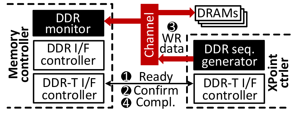
To implement the reverse-write function, we also introduce a DDR monitor in the memory controller. Similar to XPoint, the DDR monitor module enables the memory controller to monitor the memory channel and extract request information from the communication between XPoint and DRAM. Figure 12 shows the implementation details of the reverse-write function. Before XPoint starts the reverse-write function, the XPoint controller sends a ready signal to notify the memory controller to snarf data from the memory channel (). The memory controller then stops issuing new memory requests, enables the DDR monitor, and then sends a confirmation signal to the XPoint controller (). Afterwards, the memory controller snarfs the data from the memory channel, while XPoint writes data to DRAM (). Once XPoint sends a completion signal to the memory controller (), the memory controller serves the requests with the collected data.
V-B Half-coupled Micro Ring Resonator
Figure 13a shows our approach of generating dual routes to support auto-read/write and reverse-write functions. To snarf messages from the optical channel, the photonic receiver of XPoint tunes its resonance wavelength to , whose frequency shifts slightly from the message-carrying wavelength . Due to this wavelength shift method, the photonic receiver partially couples the laser light of wavelength . Thus, the remaining laser light traverses from XPoint to DRAM and its data are detected by DRAM’s photonic detector.
Figure 14 shows how our Ohm-GPU can leverage the half-coupled MRR and WOM coding to generate our dual routes for the swap function. Specifically, by referring the data-code mapping table, the transmitters of the target memory and the XPoint controllers can encode their data into 1st and 2nd write codes, respectively. The write codes are then modulated in the same light signals, which will be detected and decoded by the corresponding receivers. In the figure, the memory and XPoint1 controllers send data to XPoint0 and DRAM, respectively. When the memory controller transfers data “10” to XPoint0, the target data is encoded into a write code “010” and modulated into a laser light (). The half-coupled MRR-based receiver (HCMRR) of XPoint0 controller gets the laser light and decodes the write code to data “10”. This process consumes the laser light by half, which is “1”. XPoint1 controller can modulate its own data “01” in the same laser light, which turns the light bits to “11” (). DRAM can decode the laser light to retrieve data “01” by referring to the data-code mapping table.
To fully utilize bandwidth of the optical channel, we propose an aggressive approach to multiplex the data of memory requests and data migration requests on the same optical channel, which is shown in Figure 13b. Specifically, when modulating electrical bit ‘0’ as light bit, the transmitter in memory controller does not tune MRR to fully couple the laser light. Instead, the photonic transmitter tunes its resonance wavelength to , reducing the strength of the laser light by half. For example, a data stream of “00110” is modulated as “11” in terms of laser light strength. The photonic detector can identify bits 0 or 1 based on the light strength. Note that the photonic detector in XPoint also modulates the resonance wavelength to , which partially couples the laser light. At this juncture, the remaining laser light maintains at least one fourth of its original transmission power (“” in the example). The laser light continues to traverse between XPoint and DRAM. The transmitter of XPoint can modulate its own data stream “10101” in the remaining laser light by tuning MRR to fully-coupled or non-coupled. After modulation, the strength of the laser light becomes “00”. The photonic detector in DRAM fully couples the laser light and detects the data stream of “10101” by checking the light strength.
V-C Optical Channel Optimization for Low Cost
Creating dual routes to support auto-read/write, write-reverse and swap functions in any memory device requires at least three transmitters and three receivers in DRAM, and two transmitters and three receivers in XPoint. Figure 15a shows a general optical channel design. Specifically, DRAM and XPoint need to employ a pair of MRR-based photonic transmitter and receiver (i.e., T3, R8, T5, R6, T7 and R5 in Figure 15a) to support conventional photonic communication. While both DRAM and XPoint need to employ half-coupled MRR-based photonic receivers in both the forward path and backward path to enable auto-read/write function (i.e., R1, R2, R3, R4, R7 and R11), DRAM needs half-coupled MRR-based photonic receivers in the backward path to enable write-reverse function (i.e., R4 and R7). Lastly, to support data swap function in the dual routes, the half-coupled MRR-based photonic transmitters should be employed in DRAM and XPoint (i.e., T4, T6 and T8). While the photonic transmitters of T9, T10 and T11 are not necessary, they can improve the parallelism of scheduling memory requests and data swap function in parallel. We further reduce the number of MRRs based on the characteristics of different operational modes in heterogeneous memory. Specifically, planar memory mode only needs data swap function and two-level memory mode only needs auto-read/write and reverse-write functions. Figure 15b shows the MRR deployment in different operational modes. Our customized design can reduce the number of required MRRs by 58% and 42% in planar and two-level memory modes, respectively, compared to the general design. Note that, for simplicity, only a pair of DRAM and XPoint is depicted in the figure. But our analysis can be applied to any number of DRAM and XPoint.
VI Evaluation
Simulation methodology. We implement Ohm-GPU atop a GPU simulator (MacSim) [31]. To explore a full design space of optical network based heterogeneous memory subsystems, we replace six 32-bit electrical memory channels with a single optical channel as default. This optical channel configuration can provide the same bandwidth as the traditional electrical memory channels. Note that the optical channel’s bandwidth is scalable as we can increase the number of optical waveguides and wavelengths. The important parameters of our optical channel are configured based on [38]. Specifically, we adopt the static channel division policy to create six virtual channels to connect different memory devices, which matches with the number of memory controllers inside a GPU. Each virtual channel has a 16-bit data bus width and runs on 30 GHz. We then model XPoint and integrate it into MacSim. Its latency values are derived from the real XPoint-based NVDIMM performance measurement [27]. The default memory capacity of the baseline GPU is 24GB, which is the same as the memory capacity of NVIDIA K80 GPU [48]. We configure the capacity ratios of DRAM and XPoint as 1:8 and 1:64 to achieve the optimal performance [28] and maximum capacity of the GPU heterogeneous memory system, respectively. The detailed configurations are given in Table I. Considering that the simulation speed of an architectural simulator is up to 1000 slower than native-execution, we reduce the memory footprints of executed workloads to 8GB and scale down the GPU memory capacity by 12. This is a common practice in architectural studies [1].
| GPU configuration | Memory configuration | ||
| SM/freq. | 16/1.2 GHz | tRCD (DRAM) | 25 ns |
| L1 cache | 48KB, 6-way, private | tRP (DRAM) | 10 ns |
| L2 cache | 6MB, 8-way, shared | tCL (DRAM) | 11 ns |
| Electrical channels | 6 channels/32-bit/15 GHz | PRAM read | 190 ns |
| Optical channel configuration | PRAM write | 763 ns | |
| Channel width | 96 bits | tRRD | 5 ns |
| Frequency | 30 GHz | Optical power model | |
| Strategy | Static channel division | MRR tuning power | 200 fJ/bit |
| Virtual channel | 6 | Filter drop | 1.5 dB |
| DRAM : OP-DIMM capacity | Waveguide loss | 0.3 dB/cm | |
| Planar memory | 1:8, 108GB | Optical splitter | 0.2 dB |
| Two-level memory | 1:64, 390GB | Detector/Modulator | 0.1/01 dB |
| Apps | APKI | Read ratio | Benchmark | Apps | APKI | Read ratio | Benchmark |
|---|---|---|---|---|---|---|---|
| backp | 30 | 0.53 | [10] | bfsdata | 84 | 0.95 | [42] |
| lud | 20 | 0.52 | [10] | bfstopo | 25 | 0.97 | [42] |
| GRAMS | 266 | 0.7 | [54] | gctopo | 93 | 0.99 | [42] |
| FDTD | 86 | 0.7 | [54] | pagerank | 599 | 0.99 | [42] |
| betw | 193 | 0.99 | [42] | sssp | 103 | 0.98 | [42] |
Heterogeneous memory platforms. We implement seven different GPU platforms: (1) Origin: a baseline GPU architecture with a DRAM based memory system; (2) Hetero: a baseline GPU architecture employing an electrical channel integrated heterogeneous memory system. Hetero leverages the memory controller to migrate data between DRAM and XPoint; (3) Ohm-base: a baseline GPU architecture employing an optical network integrated heterogeneous memory system; (4) Auto-rw: a GPU integrating the auto-read/write function into Ohm-base; (5) Ohm-WOM: a GPU platform enabling auto-read/write, reverse-write and swap functions for Ohm-base. This platform integrates WOM coding to enable dual routes for swap function; (6) Ohm-BW: compared to Ohm-WOM, it replaces WOM coding with half-coupled MRR-based transmitters. Lastly, we configure an Oracle GPU platform that employs 108GB and 390GB DRAM in planar and two-level memory modes, respectively.
Workloads and energy model. We select ten representative workloads from [42, 10, 54], which are classified as read/write-intensive and compute/memory-intensive. The details of our evaluated workloads are shown in Table II. We also set up power models of DRAM, XPoint and optical channel to estimate the energy consumption of our Ohm memory system. Specifically, we adopt an empirical DRAM power model from [37] to estimate the DRAM power consumption in our simulation, while getting the average power and burst power of XPoint from [28]. Our power model of the optical channel (inspired by [38]) includes MRR tuning power and power loss in each optical component (e.g., filter drop loss, waveguide loss and detector loss). The details are given in Table I. Note that the bit error rate (BER) of an optical network is proportional to the sensing power of the photonic receiver [39]. To achieve a reliable end-to-end communication between the memory controllers and the DRAM/XPoint modules, we adopt the default laser light power of a single wavelength (0.73 mW) from [38], which can guarantee bit error rate (BER) under 10-15. To meet the reliability requirements, we also increase the laser light power of Auto-rw, Ohm-WOM and Ohm-BW by 2, 2 and 4, respectively.


VI-A Overall Performance Analysis
IPC. Figure 16 shows the IPC values of different GPU platforms under various workloads, normalized to Ohm-base. Due to the relatively small memory size, Origin invokes data copies between the host and the GPU more frequently. As a result, Origin degrades the overall performance, compared to Hetero, by 42%. Since the optical network in our default configuration has the same bandwidth as electrical memory channels (cf. Table I), Hetero and Ohm-base exhibit similar performance each other. Nevertheless, Ohm-base consumes a lower power and less area space than Hetero (cf. Section VI-B). Note that Ohm-base can significantly outperform Hetero by employing multiple waveguides which will be discussed in Section VI-B. Auto-rw improves the performance by 9% and 4%, respectively, in planar and two-level memory modes, compared to Ohm-base. This is because Auto-rw leverages the auto-read/write function to automate the data transfers from DRAM to XPoint without the interference from the memory controller. On the other hand, Ohm-WOM can improve the performance by 18% and 16%, compared to Auto-rw, in the two operational modes. Specifically, Ohm-WOM in planar memory mode adopts the swap function to fully decouple the memory controller from the management of data migration. Ohm-WOM in planar memory mode also hides the impact of data migration on latency-critical read requests by issuing the data migration with write requests at background. By adopting this approach, the performance of Ohm-WOM is further increased by 4%. Lastly, Ohm-WOM in two-level memory mode automates the data transfer from XPoint to DRAM with the reverse-write function, which reduce the optical channel traffic. Compared to Ohm-WOM, Ohm-BW further improves the performance by 4% in the planar mode. This is because Ohm-BW increases the effective bandwidth of optical channels for the memory requests, thereby improving the overall performance. As DRAM delivers up to 6 higher throughput than XPoint [28], Oracle outperforms all the evaluated GPU platforms that employ heterogeneous memory systems (i.e., Hetero, Ohm-base, Auto-rw, Ohm-WOM and Ohm-BW). Note that Ohm-BW achieves 88% of the ideal GPU performance (Oracle) with a much lower cost (cf. Section VI-B for details).


Memory latency analysis. Figure 17 shows the average memory latencies of different GPU platforms under various workloads, normalized to Ohm-base. Auto-rw can reduce the average memory latencies by 14% and 4%, respectively, in planar and two-level memory modes, compared to Ohm-base. This is because Auto-rw can reduce the time of the optical channel to do data migration, so that memory devices can use the optical channel earlier to serve the regular memory requests. Ohm-WOM in planar memory mode leverages swap function to schedule the data migration through the dual routes in parallel with the memory requests, which does not occupy the optical channel. Thus, Ohm-WOM achieves the minimum memory access latency, which is 28% shorter than Auto-rw, in planar memory mode. Similarly, the benefit of memory latency reduction brought by Ohm-WOM in two-level memory mode is 24%, compared to Auto-rw. Although the reverse-write function in Ohm-WOM cannot shorten the latency of serving the memory requests from XPoint, the reverse-write function leverages the dual routes to reduce the latency of copying data from XPoint to DRAM, making the data migration procedure complete earlier. Compared to Ohm-WOM, Ohm-BW can serve the memory requests faster when swap function is invoked. Therefore, Ohm-BW further reduces the memory latency by 6% in planar memory mode. Ohm-BW reduces the performance gap between a heterogeneous memory system and an ideal memory system from 67% to 18%. This is because Ohm-BW effectively leverage its DRAM cache to serve the most incoming memory requests.
Optical channel usage. Figure 18 shows the fraction of the optical channel bandwidth consumed by data migration in different memory platforms. As Auto-rw can partially do the data migration in the dual routes, it can reduce the bandwidth usage for data migration by 8% and 17%, respectively, in planar and two-level memory modes. Ohm-WOM in planar memory mode further reduces the bandwidth usage by 54% because it performs most of data migrations in the dual routes. Ohm-WOM in the two-level memory mode can fully eliminate the optical channel occupancy caused by data migration. This is because the auto-read/write and reverse-write functions migrate the data in an independent route, when DRAM and XPoint serve the memory requests.
Energy consumption. Figure 19 shows the energy consumption of different components within the memory systems of the evaluated GPU platforms. Compared to Hetero, Ohm-base replaces the electrical memory channels with an optical channel, which can reduce the DMA’s power by 57%, on average. As the user applications generate a fixed amount of memory requests to DRAM, the dynamic DRAM energy to serve the memory requests is the same as those of Ohm-base, Auto-rw, Ohm-WOM and Ohm-BW. On the other hand, the static DRAM energy is proportional to the total execution time when DRAM is powered on. As Ohm-WOM can reduce the execution time of user applications, it, on average, can reduce the static DRAM energy by 19% and 11%, respectively, compared to Ohm-base and Auto-rw. Similar to dynamic DRAM energy, the XPoint in different heterogeneous memory platforms serve the same number of memory requests, which consumes the same amount of energy. Auto-rw, Ohm-WOM and Ohm-BW consume higher optical channel energy than Ohm-base. This is because the laser source needs to increase its power to meet the sensing accuracy of the photonic detectors in the dual routes. As laser power has a minor impact on the energy cost than DRAM and XPoint, Ohm-WOM still decreases the overall energy consumption by 2% and 1% in planar and two-level memory modes, against Ohm-base.


VI-B Sensitive testing, reliability and Overhead
Sensitive tests. While a single optical waveguide can achieve the bandwidth same as electrical memory channels of 192 lanes, Ohm-GPU can employ multiple optical waveguides under the same area constrains as the electrical memory channels. Figure 20a shows the performance improvement brought by multiple optical waveguides in Ohm-GPU. Ohm-base with 8 optical waveguides improves the system performance than Hetero, by 41%, on average. This is because employing multiple optical waveguides can significantly reduce the DMA latency of the heterogeneous memory system. Ohm-BW also benefits from the increased number of optical waveguides. The performance improvement can be 17%.
Reliability. We evaluate the data integrity of the end-to-end communication in various GPU memory systems, and the results are shown in Figure 20b. When serving memory requests, Ohm-base can achieve BER as low as 7.210-16 with our default configuration of laser light power. Since Ohm-WOM and Ohm-BW deploy more MRR-based modulators and detectors in the optical infrastructure for the auto-read/write and swap functions, modulating and detecting data in these MRRs can attenuate the strength of laser signals (cf. optical power model in Table I). To compensate for the laser power loss, we increase the powers of the laser source by 2 and 4 in Ohm-WOM and Ohm-BW, respectively. The measured BER of auto-read/write and swap functions are 6.110-16 and 9.910-16, respectively, in Ohm-WOM, while the worst BER in Ohm-BW is 9.310-16. To sum up, the optical channel of Ohm-GPU satisfies the reliability requirement of 10-15 BER.
| Modes | Planar memory | Two-level memory | ||
|---|---|---|---|---|
| DRAM | 1GB x 12, $140 | 1GB x 6, $70 | ||
| XPoint | 8GB x 12, $125 | 32GB x 12, $499 | ||
| Modulators | Detectors | Modulators | Detectors | |
| Ohm-base | 2,112/$3 | 2,112/$3 | 2,368/$3 | 2,368/$3 |
| Ohm-BW | 2,176/$3 | 3,136/$5 | 2,368/$3 | 4,928/$7 |
| VCSEL | $100 | |||
Overhead analysis. Table III lists the estimated cost of the key components in different platforms. We configure up to 24 memory devices in a GPU, while the number of DRAM and XPoint chips are set to follow the capacity ratio listed in Table I. The price of memory devices are calculated based on [19, 62]. We refer to Figure 15 to calculate the total number of MRRs required in each memory platform. The fabrication cost of MRRs is estimated based on [22]. Although Ohm-BW employs 41% more MRRs (at the cost of $4) than Ohm-base to support the dual routes in the optical channel, Ohm-BW improves the performance by 20%, demonstrating higher performance/cost ratio. In addition to optical components, Ohm-BW also employs a DDR monitor and DDR sequence generator in the memory controller and the XPoint controller, respectively. The DDR monitor is comprised of control logic and a few registers, which enable/disable a DDR interface controller to receive data from the data bus, while the DDR sequence generator converts the memory requests into DDR packets. Our implementation of DDR sequence generators requires 2.8K LUTs and 4.7K flip-flops in FPGA, whose cost is negligible to the XPoint controller. Considering the launch price of NVIDIA K80 GPU ($5k), planar and two-level memory modes enabled Ohm-BW only increase total cost by 7.6% and 13.5%, respectively. We also evaluate the cost-performance (CP) ratio of NVIDIA K80 GPU (Origin), our Ohm-GPU (Ohm-BW) and an ideal GPU (Oracle), and the results are shown in Figure 21. The CP ratio of Ohm-BW is 155% and 24% higher than that of Origin and Oracle, respectively, indicating that the performance benefits brought by Ohm-GPU overwhelms its cost overhead.
VII Related Work

Optical network. To address an expensive energy cost and limited scalability of electrical wires, multiple prior work [16, 15, 75, 64, 18, 6, 38] have proposed to integrate optical network into the memory system as a replacement of electrical wires. Specifically, [16, 15, 75] propose to substitute the traditional electrical network-on-chip with optical on-chip crossbar interconnects in a 3D-stacked GPU, which can improve throughput of interconnect network while saving its operating power. On the other hand,[64] configures the optical network for both inter-core and off-chip memory communication, which can easily achieve 20 TB/s bandwidth with lower power. In addition to the benefits of bandwidth and power, [18] reports a significant network latency reduction and memory capacity expansion by replacing the store-and-forward network and protocol in FB-DIMM with the low-latency optical network. [6] and [38] further optimize the optical memory subsystem by revising either the memory architecture or the optical network. [6] proposes to reduce the number of activated bits in each DRAM bank to reduce power consumption, while [38] proposes to dynamically assign multiple wavelengths as virtual channels to connect to different memory devices, which can mitigate the overhead of rank-to-rank switch delay. While the prior research achieves great progress in integrating the optical network in a homogeneous memory, none of them consider using optical network to address the challenges of a heterogeneous memory. To the best of our knowledge, Ohm-GPU is the first to address the data migration issue in the heterogeneous memory by leveraging the unique characteristics of optical network. To mitigate the impact of data migration on optical network, Ohm-GPU modified the designs of both optical network and heterogeneous memory architecture.
Heterogeneous memory. There are many prior studies [4, 20, 65, 24, 35] oriented towards achieving the balance of high performance and large capacity in the memory system by employing both fast-but-small memory and large-but-slow memory. [4] proposes to group DRAM and PRAM as a heterogeneous memory, while [65] places SLC PRAM and MLC PRAM together. However, all these studies adopt a legacy PRAM model, which uses a low-power protocol (LPDDR2-NVM) and exhibits a read/write latency close to DRAM latency. Recently, [28] and [51] reveal the performance of combining DRAM and XPoint-based Optane DC PMM in a real computing environment. However, their research is limited to use Optane DC PMM as a black box without digging deeper into the internal architecture. In contrast, we revealed the key component designs of the heterogeneous memory. We also explored the design space of XPoint to collaborate with optical network to address the data migration issue.
Data migration. There also exist many studies that try to mitigate the impact of data migration on the memory channel. [58] proposes to leverage the data bus within each DRAM rank to perform intra-bank or inter-bank data migration. While data migration in this approach does not occupy the memory channel, the data migration is constrained to operate within the DRAM rank. Although [65] allows data migration across two PRAM ranks in a lightweight way, the proposed approach relies on a unique architecture where the two PRAM ranks share the same row buffers. While the techniques proposed in both prior work are designed for homogeneous memory, our Ohm-GPU makes it feasible to mitigate the impact of data migration across different DIMMs by leveraging the dual routes in the optical network.
VIII Conclusion
In this work, we propose Ohm-GPU, a new design of optical network for heterogeneous memory integrated GPU, which can mitigate the impact of data migration on optical channel. Specifically, Ohm-GPU decouples the memory controller from the management of the data migration and leverages the dual routes in optical channel to prevent data migration from occupying the memory channel. Our Ohm-GPU can improve the performance by 181% and 27%, compared to a DRAM-based GPU memory system and the baseline optical network based heterogeneous memory system, respectively.
IX Acknowledgement
This research is mainly supported by NRF 2021R1AC4001773 and IITP 2021-0-00524. The work is also supported in part by KAIST start-up package (G01190015), and Samsung (G01200447). Other product names used in this publication are for identification purposes only and may be trademarks of their respective companies. Myoungsoo Jung is the corresponding author.
References
- [1] M. Alian, A. H. Abulila, L. Jindal, D. Kim, and N. S. Kim, “Ncap: Network-driven, packet context-aware power management for client-server architecture,” in 2017 IEEE International Symposium on High Performance Computer Architecture (HPCA). IEEE, 2017, pp. 25–36.
- [2] AMD, “High-bandwidth memory (hbm),” https://www.amd.com/system/files/documents/high-bandwidth-memory-hbm.pdf, 2015.
- [3] M. Aoyama, K. Ogasawara, M. Sugawara, T. Ishibashi, T. Ishibashi, S. Shimoyama, K. Yamaguchi, T. Yanagita, and T. Noma, “3 gbps, 5000 ppm spread spectrum serdes phy with frequency tracking phase interpolator for serial ata,” in 2003 Symposium on VLSI Circuits. Digest of Technical Papers (IEEE Cat. No. 03CH37408). IEEE, 2003, pp. 107–110.
- [4] S. Baek, H. G. Lee, C. Nicopoulos, and J. Kim, “A dual-phase compression mechanism for hybrid dram/pcm main memory architectures,” in Proceedings of the Great lakes symposium on VLSI. ACM, 2012, pp. 345–350.
- [5] M. Bahadori, S. Rumley, D. Nikolova, and K. Bergman, “Comprehensive design space exploration of silicon photonic interconnects,” Journal of Lightwave Technology, vol. 34, no. 12, pp. 2975–2987, 2016.
- [6] S. Beamer, C. Sun, Y.-J. Kwon, A. Joshi, C. Batten, V. Stojanović, and K. Asanović, “Re-architecting dram memory systems with monolithically integrated silicon photonics,” in ACM SIGARCH Computer Architecture News, vol. 38, no. 3. ACM, 2010, pp. 129–140.
- [7] R. G. Beausoleil, P. J. Kuekes, G. S. Snider, S.-Y. Wang, and R. S. Williams, “Nanoelectronic and nanophotonic interconnect,” Proceedings of the IEEE, vol. 96, no. 2, pp. 230–247, 2008.
- [8] K. Bergman, L. P. Carloni, A. Biberman, J. Chan, and G. Hendry, Photonic network-on-chip design. Springer, 2014.
- [9] L.-P. Chang, “On efficient wear leveling for large-scale flash-memory storage systems,” in Proceedings of the 2007 ACM symposium on Applied computing, 2007, pp. 1126–1130.
- [10] S. Che, M. Boyer, J. Meng, D. Tarjan, J. W. Sheaffer, S.-H. Lee, and K. Skadron, “Rodinia: A benchmark suite for heterogeneous computing,” in 2009 IEEE international symposium on workload characterization (IISWC). Ieee, 2009, pp. 44–54.
- [11] N. Dahad, “Addressing memory wall is key to edge-based ai,” https://www.eetimes.com/document.asp?doc_id=1333456, 2018.
- [12] G. Dhiman, R. Ayoub, and T. Rosing, “Pdram: A hybrid pram and dram main memory system,” in 2009 46th ACM/IEEE Design Automation Conference. IEEE, 2009, pp. 664–669.
- [13] M. Feldman, “Revisiting the memory wall,” https://www.hpcwire.com/2009/02/19/revisiting_the_memory_wall/, 2009.
- [14] K. Gai, M. Qiu, and H. Zhao, “Cost-aware multimedia data allocation for heterogeneous memory using genetic algorithm in cloud computing,” IEEE transactions on cloud computing, 2016.
- [15] N. Goswami, Z. Li, R. Shankar, and T. Li, “Exploring silicon nanophotonics in throughput architecture,” IEEE Design & Test, vol. 31, no. 5, pp. 18–27, 2014.
- [16] N. Goswami, Z. Li, A. Verma, R. Shankar, and T. Li, “Integrating nanophotonics in gpu microarchitecture,” in Proceedings of the 21st international conference on Parallel architectures and compilation techniques, 2012, pp. 425–426.
- [17] A. Gupta, Y. Kim, and B. Urgaonkar, “Dftl: a flash translation layer employing demand-based selective caching of page-level address mappings,” Acm Sigplan Notices, vol. 44, no. 3, pp. 229–240, 2009.
- [18] A. Hadke, T. Benavides, S. B. Yoo, R. Amirtharajah, and V. Akella, “Ocdimm: Scaling the dram memory wall using wdm based optical interconnects,” in 2008 16th IEEE Symposium on High Performance Interconnects. IEEE, 2008, pp. 57–63.
- [19] H. Hagedoorn, “Gddr6 significantly more expensive than gddr5,” https://www.guru3d.com/news-story/gddr6-significantly-more-expensive-than-gddr5.html, 2019.
- [20] T. J. Ham, B. K. Chelepalli, N. Xue, and B. C. Lee, “Disintegrated control for energy-efficient and heterogeneous memory systems,” in 2013 IEEE 19th International Symposium on High Performance Computer Architecture (HPCA). IEEE, 2013, pp. 424–435.
- [21] Hamza, “Hbm2 vs gddr6 memory comparison,” https://flashbang.biz/hbm2-vs-gddr6-memory-specification-and-full-comparison/, 2019.
- [22] T. Hausken, “Breaking the cost barrier,” https://www.osa-opn.org/home/articles/volume_26/july_august_2015/departments/breaking_the_cost_barrier/, 2015.
- [23] J. Hruska, “Optane dc persistent memory offers up to 512gb per dimm,” https://www.extremetech.com/computing/288854-optane-dc-persistent-memory-offers-up-to-512gb-per-dimm, 2019.
- [24] W. Hwang and K. H. Park, “Hmmsched: Hybrid main memory-aware task scheduling on multicore systems,” in Proceedings of international conference on future computational technologies and applications, vol. 52, 2013.
- [25] Intel, “Intel optane dc persistent memory,” https://www.intel.com/content/www/us/en/architecture-and-technology/optane-dc-persistent-memory.html, 2018.
- [26] ——, “How to overclock ram,” https://www.intel.com/content/www/us/en/gaming/resources/overclock-ram.html, 2019.
- [27] J. Izraelevitz, J. Yang, L. Zhang, J. Kim, X. Liu, A. Memaripour, Y. J. Soh, Z. Wang, Y. Xu, S. R. Dulloor et al., “Basic performance measurements of the intel optane dc persistent memory module,” arXiv preprint arXiv:1903.05714, 2019.
- [28] J. Izraelevitz, J. Yang, L. Zhang, J. Kim, X. Liu, A. Memaripour, Y. J. Soh, Z. Wang, Y. Xu, S. R. Dulloor, J. Zhao, and S. Swanson, “Basic performance measurements of the intel optane dc persistent memory module,” https://arxiv.org/abs/1903.05714, 2019.
- [29] U. Kang, H.-S. Yu, C. Park, H. Zheng, J. Halbert, K. Bains, S. Jang, and J. S. Choi, “Co-architecting controllers and dram to enhance dram process scaling,” in The memory forum, vol. 14, 2014.
- [30] P. Kennedy, “A close look at intel optane dc persistent memory modules,” https://www.servethehome.com/a-close-look-at-intel-optane-dc-persistent-memory-modules/, 2018.
- [31] H. Kim, J. Lee, N. B. Lakshminarayana, J. Sim, J. Lim, and T. Pho, “Macsim: A cpu-gpu heterogeneous simulation framework user guide,” Georgia Institute of Technology, 2012.
- [32] J. Kim, J. M. Kim, S. H. Noh, S. L. Min, and Y. Cho, “A space-efficient flash translation layer for compactflash systems,” IEEE Transactions on Consumer Electronics, vol. 48, no. 2, pp. 366–375, 2002.
- [33] Y. Kim, “Architectural techniques to enhance dram scaling,” Ph.D. dissertation, figshare, 2015.
- [34] Y. Kim, R. Daly, J. Kim, C. Fallin, J. H. Lee, D. Lee, C. Wilkerson, K. Lai, and O. Mutlu, “Flipping bits in memory without accessing them: An experimental study of dram disturbance errors,” in ACM SIGARCH Computer Architecture News, vol. 42, no. 3. IEEE Press, 2014, pp. 361–372.
- [35] S. Kwon, D. Kim, Y. Kim, S. Yoo, and S. Lee, “A case study on the application of real phase-change ram to main memory subsystem,” in 2012 Design, Automation & Test in Europe Conference & Exhibition (DATE). IEEE, 2012, pp. 264–267.
- [36] C. Lee, W. Shin, D. J. Kim, Y. Yu, S.-J. Kim, T. Ko, D. Seo, J. Park, K. Lee, S. Choi et al., “Nvdimm-c: A byte-addressable non-volatile memory module for compatibility with standard ddr memory interfaces,” in 2020 IEEE International Symposium on High Performance Computer Architecture (HPCA). IEEE, 2020, pp. 502–514.
- [37] J. Leng, T. Hetherington, A. ElTantawy, S. Gilani, N. S. Kim, T. M. Aamodt, and V. J. Reddi, “Gpuwattch: enabling energy optimizations in gpgpus,” ACM SIGARCH Computer Architecture News, vol. 41, no. 3, pp. 487–498, 2013.
- [38] Z. Li, R. Zhou, and T. Li, “Exploring high-performance and energy proportional interface for phase change memory systems,” in 2013 IEEE 19th International Symposium on High Performance Computer Architecture (HPCA). IEEE, 2013, pp. 210–221.
- [39] A. Melloni, M. Martinelli, G. Cusmai, and R. Siano, “Experimental evaluation of ring resonator filters impact on the bit error rate in non return to zero transmission systems,” Optics communications, vol. 234, no. 1-6, pp. 211–216, 2004.
- [40] R. Micheloni, A. Marelli, and K. Eshghi, Inside solid state drives (SSDs). Springer, 2013.
- [41] R. Morris, E. Jolley, and A. K. Kodi, “Extending the performance and energy-efficiency of shared memory multicores with nanophotonic technology,” IEEE Transactions on Parallel and Distributed Systems, vol. 25, no. 1, pp. 83–92, 2013.
- [42] L. Nai, Y. Xia, I. G. Tanase, H. Kim, and C.-Y. Lin, “Graphbig: understanding graph computing in the context of industrial solutions,” in SC’15: Proceedings of the International Conference for High Performance Computing, Networking, Storage and Analysis. IEEE, 2015, pp. 1–12.
- [43] P. J. Nair, D.-H. Kim, and M. K. Qureshi, “Archshield: Architectural framework for assisting dram scaling by tolerating high error rates,” in ACM SIGARCH Computer Architecture News, vol. 41, no. 3. ACM, 2013, pp. 72–83.
- [44] B. Nale, R. K. Ramanujan, M. P. SWAMINATHAN, T. Thomas, and T. Polepeddi, “Memory channel that supports near memory and far memory access,” May 7 2019, uS Patent 10,282,322.
- [45] NIVIDIA, “Nvidia kepler next generation cuda compute architecture,” Computer system, vol. 26, pp. 63–72, 2012.
- [46] Nvidia, “Nvidia tesla v100 gpu architecture,” http://images.nvidia.com/content/volta-architecture/pdf/volta-architecture-whitepaper.pdf, 2017.
- [47] NVIDIA, “Nvidia turing gpu architecture,” https://www.nvidia.com/content/dam/en-zz/Solutions/design-visualization/technologies/turing-architecture/NVIDIA-Turing-Architecture-Whitepaper.pdf, 2019.
- [48] Nvidia, “Nvidia tesla k80: The world most popular gpu,” https://www.nvidia.com/en-gb/data-center/tesla-k80/, 2021.
- [49] C. Nvidia, “Nvidia’s next generation cuda compute architecture: Fermi,” Comput. Syst, vol. 26, pp. 63–72, 2009.
- [50] G. Park, M. Kwon, P. Mahapatra, M. Swift, and M. Jung, “BIBIM: A prototype multi-partition aware heterogeneous new memory,” in 10th USENIX Workshop on Hot Topics in Storage and File Systems (HotStorage 18), 2018.
- [51] O. Patil, L. Ionkov, J. Lee, F. Mueller, and M. Lang, “Performance characterization of a dram-nvm hybrid memory architecture for hpc applications using intel optane dc persistent memory modules,” in Proceedings of the International Symposium on Memory Systems. ACM, 2019, pp. 288–303.
- [52] J. T. Pawlowski, “Hybrid memory cube (hmc),” in 2011 IEEE Hot chips 23 symposium (HCS). IEEE, 2011, pp. 1–24.
- [53] E. Peter, A. Thomas, A. Dhawan, and S. R. Sarangi, “Active microring based tunable optical power splitters,” Optics Communications, vol. 359, pp. 311–315, 2016.
- [54] L.-N. Pouchet, “Polybench: The polyhedral benchmark suite,” URL: http://www. cs. ucla. edu/pouchet/software/polybench, 2012.
- [55] M. K. Qureshi, J. Karidis, M. Franceschini, V. Srinivasan, L. Lastras, and B. Abali, “Enhancing lifetime and security of pcm-based main memory with start-gap wear leveling,” in 2009 42nd Annual IEEE/ACM international symposium on microarchitecture (MICRO). IEEE, 2009, pp. 14–23.
- [56] R. K. Ramanujan, G. J. Hinton, and D. J. Zimmerman, “Dynamic partial power down of memory-side cache in a 2-level memory hierarchy,” Oct. 9 2014, uS Patent App. 13/994,726.
- [57] Samsung, “Ultra-low latency with samsung z-nand ssd,” Ultra-Low_Latency_with_Samsung_Z-NAND_SSD-0.pdf, 2017.
- [58] V. Seshadri, Y. Kim, C. Fallin, D. Lee, R. Ausavarungnirun, G. Pekhimenko, Y. Luo, O. Mutlu, P. B. Gibbons, M. A. Kozuch et al., “Rowclone: fast and energy-efficient in-dram bulk data copy and initialization,” in Proceedings of the 46th Annual IEEE/ACM International Symposium on Microarchitecture. ACM, 2013, pp. 185–197.
- [59] A. Shacham, K. Bergman, and L. P. Carloni, “On the design of a photonic network-on-chip,” in First International Symposium on Networks-on-Chip (NOCS’07). IEEE, 2007, pp. 53–64.
- [60] ——, “Photonic networks-on-chip for future generations of chip multiprocessors,” IEEE Transactions on Computers, vol. 57, no. 9, pp. 1246–1260, 2008.
- [61] M. M. Shulaker, T. F. Wu, A. Pal, L. Zhao, Y. Nishi, K. Saraswat, H.-S. P. Wong, and S. Mitra, “Monolithic 3d integration of logic and memory: Carbon nanotube fets, resistive ram, and silicon fets,” in 2014 IEEE International Electron Devices Meeting. IEEE, 2014, pp. 27–4.
- [62] B. Tallis, “The intel optane ssd 900p 480gb review: Diving deeper into 3d xpoint,” https://www.anandtech.com/show/12136/the-intel-optane-ssd-900p-480gb-review, 2017.
- [63] T. Thomas, “Gddr6 vs hbm2 memory,” https://www.techsiting.com/gddr6-vs-hbm2/, 2019.
- [64] D. Vantrease, R. Schreiber, M. Monchiero, M. McLaren, N. P. Jouppi, M. Fiorentino, A. Davis, N. Binkert, R. G. Beausoleil, and J. H. Ahn, “Corona: System implications of emerging nanophotonic technology,” in ACM SIGARCH Computer Architecture News, vol. 36, no. 3. IEEE Computer Society, 2008, pp. 153–164.
- [65] H. Wang, J. Zhang, S. Shridhar, G. Park, M. Jung, and N. S. Kim, “Duang: Fast and lightweight page migration in asymmetric memory systems,” in 2016 IEEE International Symposium on High Performance Computer Architecture (HPCA). IEEE, 2016, pp. 481–493.
- [66] J. Yang, J. Kim, M. Hoseinzadeh, J. Izraelevitz, and S. Swanson, “An empirical guide to the behavior and use of scalable persistent memory,” in 18th USENIX Conference on File and Storage Technologies (FAST 20), 2020, pp. 169–182.
- [67] J. H. Yoon, H. C. Hunter, and G. A. Tressler, “Flash & dram si scaling challenges, emerging non-volatile memory technology enablement-implications to enterprise storage and server compute systems,” Flash Memory Summit, 2013.
- [68] J. Zhang, D. Donofrio, J. Shalf, M. T. Kandemir, and M. Jung, “Nvmmu: A non-volatile memory management unit for heterogeneous gpu-ssd architectures,” in 2015 International Conference on Parallel Architecture and Compilation (PACT). IEEE, 2015, pp. 13–24.
- [69] J. Zhang and M. Jung, “Zng: Architecting gpu multi-processors with new flash for scalable data analysis,” in 2020 ACM/IEEE 47th Annual International Symposium on Computer Architecture (ISCA). IEEE, 2020, pp. 1064–1075.
- [70] J. Zhang, M. Kwon, H. Kim, H. Kim, and M. Jung, “Flashgpu: Placing new flash next to gpu cores,” in 2019 56th ACM/IEEE Design Automation Conference (DAC). IEEE, 2019, pp. 1–6.
- [71] J. Zhang, G. Park, M. M. Shihab, D. Donofrio, J. Shalf, and M. Jung, “Opennvm: An open-sourced fpga-based nvm controller for low level memory characterization,” in 2015 33rd IEEE International Conference on Computer Design (ICCD). IEEE, 2015, pp. 666–673.
- [72] L. Zhou and A. K. Kodi, “Probe: Prediction-based optical bandwidth scaling for energy-efficient nocs,” in 2013 Seventh IEEE/ACM International Symposium on Networks-on-Chip (NoCS). IEEE, 2013, pp. 1–8.
- [73] P. Zhou, B. Zhao, J. Yang, and Y. Zhang, “A durable and energy efficient main memory using phase change memory technology,” ACM SIGARCH computer architecture news, vol. 37, no. 3, pp. 14–23, 2009.
- [74] Q. Zhu, T. Graf, H. E. Sumbul, L. Pileggi, and F. Franchetti, “Accelerating sparse matrix-matrix multiplication with 3d-stacked logic-in-memory hardware,” in 2013 IEEE High Performance Extreme Computing Conference (HPEC). IEEE, 2013, pp. 1–6.
- [75] A. K. K. Ziabari, J. L. Abellán, R. Ubal, C. Chen, A. Joshi, and D. Kaeli, “Leveraging silicon-photonic noc for designing scalable gpus,” in Proceedings of the 29th ACM on International Conference on Supercomputing, 2015, pp. 273–282.