Near-field imaging of plasmonic nanopatch antennas with integrated semiconductor quantum dots
Abstract
Plasmonic nanopatch antennas that incorporate dielectric gaps hundreds of picometers to several nanometers thick have drawn increasing attention over the past decade because they confine electromagnetic fields to grossly sub-diffraction limited volumes. Substantial control over the optical properties of excitons and color centers confined within these plasmonic cavities has already been demonstrated with far-field optical spectroscopies, but near-field optical spectroscopies are essential to an improved understanding of the plasmon-emitter interaction at the nanoscale. Here, we characterize the intensity and phase-resolved plasmonic response of isolated nanopatch antennas with cathodoluminescence microscopy. Further, we explore the distinction between optical and electron-beam spectroscopies of coupled plasmon-exciton heterostructures to identify constraints and opportunities for future nanoscale characterization and control of hybrid nanophotonic structures. While we observe substantial Purcell enhancement in time-resolved photoluminescence spectroscopies, negligible Purcell enhancement is observed in cathodoluminescence spectroscopies of hybrid nanophotonic structures. The substantial differences in measured Purcell enhancement for electron-beam and laser excitation can be understood as a result of the different selection rules for these complementary experiments. These results provide a fundamentally new understanding of near-field plasmon-exciton interactions in nanopatch antennas that is essential to myriad emerging quantum photonic devices.
I Introduction
Plasmonic heterostructures that offer grossly sub-diffraction-limited field confinement have been a topic of intense research for much of the past twenty yearsWu, Yan, and Lalanne 2021; Baumberg et al. 2019; Maier et al. 2003; Maier 2006; Brongersma, Hartman, and Atwater 2000. This nanoscale field confinement has enabled advances in optical information processingZijlstra, Chon, and Gu 2009, photocatalysisLinic, Christopher, and Ingram 2011, and plasmon enhanced sensors and spectroscopiesNie and Emory 1997; Maier 2006; Lee et al. 2021, as well as a variety of studies of plasmonic analogues to cavity quantum electrodynamicsBaumberg et al. 2019; Benz et al. 2016; Lawrie et al. 2012; Fofang et al. 2008; Akselrod et al. 2014; Akselrod et al. 2016; Huang et al. 2018. While conventional lithographically patterned plasmonic nanostructures like split ring resonatorsCubukcu et al. 2009, bowtie antennasJin and Xu 2006, nanodiscs Lawrie et al. 2012, and other nanopatterned resonators Davidson et al. 2016 can offer a sufficiently small mode volume to enable the exploration of weak and strong plasmon-exciton coupling Lawrie et al. 2012; Fofang et al. 2008; Pamu et al. 2021, the emergence of gap plasmon modes that are confined to gaps of order 1 nm has enabled substantially increased flexibility in the control of the optical properties of excitons and color centers confined within the gapBaumberg et al. 2019; Benz et al. 2016; Akselrod et al. 2014; Akselrod et al. 2016; Huang et al. 2018. Plasmonic nanogap heterostructures have been used to enhance the quantum efficiency of defect and exciton emission in the weak coupling regimeAkselrod et al. 2016; Jiang et al. 2014; Hoang, Akselrod, and Mikkelsen 2016; Huang et al. 2018; Bogdanov et al. 2018; Luo et al. 2018, to modify optical properties in the strong coupling regimeKleemann et al. 2017; Chikkaraddy et al. 2016; Qin et al. 2020, and for applications ranging from gas sensingPowell et al. 2016, water splittingXu et al. 2015, and carbon captureLu et al. 2020 to the non-invasive study of nanoparticle dynamics in liquidsBischak et al. 2017. Electrical tuning of the resonance frequency of nanogap antennas has also been demonstrated as part of the move toward more functional nanophotonic devicesHoang and Mikkelsen 2016.
While finite difference time domain (FDTD) simulations and finite element models (FEM) are widely used to simulate the near-field optical response of plasmonic cavities, inhomogeneities in the actual devices ultimately constrain the photonic response. A clear understanding of plasmonic near-field interactions is essential to uncover the structure-function relationship for nanophotonic media. Techniques such as electron energy loss spectroscopy (EELS) and cathodoluminescence (CL) microscopy are well suited to study the near-field optical properties of plasmonic heterostructuresHachtel et al. 2019; Pakeltis et al. 2021; Hachtel et al. 2018 and hybrid plasmon-emitter heterostructuresFeldman et al. 2018. In this work, we use CL microscopy to map localized and propagating plasmon modes in the proximity of silver (Ag) nanopatch antennas and analyze the effect of this plasmon mode structure on CdSe quantum dots deposited within the nanopatch antenna (NPA). We compare the results with steady state and time-resolved photoluminescence measurements. Furthermore, we perform FEM simulations that improve our understanding of the plasmonic modes observed in CL. Lastly, we observe interference between electron-beam generated transition radiation and surface plasmon polaritons scattered from the NPA. Notably, while substantial Purcell enhancement is observed in the time-resolved photoluminescence (TRPL) spectra, negligible Purcell enhancement is observed in the CL spectra as a result of different selection rules for electron-beam and optical excitations. Combining CL microscopy of nanoplasmonic modes with PL microscopy of plasmon-exciton interactions is thus essential to understanding plasmon-exciton interactions in nanopatch antennas that are essential to a plethora of emerging applications, such as light absorbers, photodetectors, and photon sources.

II Spectrum Imaging of Individual Nanopatch Antennas


The nanopatch heterostructures explored here comprise Ag nanocubes with 75-nm edges dropcast onto a 100-nm gold (Au) thin film. A 3-5 nm spacer layer is deposited between the Au film and the nanocube to minimize charge transfer and to maximize field confinement within the spacer layer. For initial spectroscopic mapping of the plasmon modes, a 3 nm ZnO spacer layer was deposited on the Au films on silicon substrates by atomic layer deposition. For subsequent spectroscopies of coupled plasmon-exciton heterostructures, a peel-and-stick technique was used to transfer gold films with sub-nm surface roughness onto a glass substrate, onto which a polyelectrolyte (PE) spacer layer (3 nm in thickness) was deposited with a dip-coating technique, and CdSe QDs were then spincast before Ag nanocube deposition. A cross-sectional schematic of the fabricated NPA heterostructures and a schematic representation of the CL collection optics are shown in Figure 1.
The nanocube’s plasmonic modes were probed directly by CL microscopy in a FEI Quattro environmental scanning electron microscope (ESEM) with a Delmic Sparc CL collection system. All data described here were acquired with a beam energy of 30 keV, and beam currents of 630-5600 pA were used depending on sample robustness. While the ESEM can operate in a high vacuum or water vapor environment, all data reported here were taken in a background pressure of 40 Pa of water vapor in order to minimize charging and carbon deposition during long spectrum image acquisitions. The NPAs display three prominent plasmon modes centered at wavelengths of 400 nm, 520 nm and 780 nm, as shown in Figure 2 for a typical nanocube. The inset shows the SEM image of the cube. The mode around 780 nm is strongest when the electron beam is in the center whereas the mode around 400 nm is strongest near the corner. The edge mode is weakly excited at the center. However, the point spectra by themselves provide only a limited understanding of the heterostructure’s plasmonic response. The edge and corner modes were previously observed in the near field with EELSGoris et al. 2014 for nanocube assemblies (different than the current nanopatch antenna system), but EELS cannot distinguish the radiative and non radiative modes, a critical requirement for hybrid plasmon-exciton heterostructures.
The spectrum images shown in Figure 3 depict the spatial distribution of distinct modes supported by the nanocube. The images shown in the left column (Figures 3(a), (e), (i)) represent the raw CL intensity at wavelengths of 380, 510, and 820 nm that best represent the corner, edge, and gap plasmon modes. However, simply plotting CL images associated with a limited number of wavelengths tends to obscure the information within the larger spectrum image. Hence, we used non-negative matrix factorization (NMF) to decompose the spectrum image into relevant spectral components. NMF has become a widely used tool for analysis of hyperspectral microscopies because it offers a computationally inexpensive approach to extract sparse, physically relevant data from multidimensional dataKonečná et al. 2021; Liu et al. 2019.
Figures 3 (b), (f) and (j) show the three most prominent modes obtained by four-component NMF, which closely match the modes identified in the raw CL intensity maps (the fourth component is described in Fig.4). The NMF spectra for each of the three components are shown in Figures 3 (c), (g) and (k). Notably, while the NMF decomposition identifies a high quality-factor corner plasmon resonance, the edge mode exhibits some additional spectral complexity, and the gap plasmon mode exhibits a clear bimodal response that is not evident in the direct intensity plot. These raw intensity plots and NMF decompositions are largely consistent with FEM simulations of the plasmonic field confinement induced by a line-current source emulating an ’electron-beam’ (as shown in the right column of Fig. 3), though they certainly exhibit the hallmarks of experimental heterogeneities.
III Plasmon interference with transition radiation
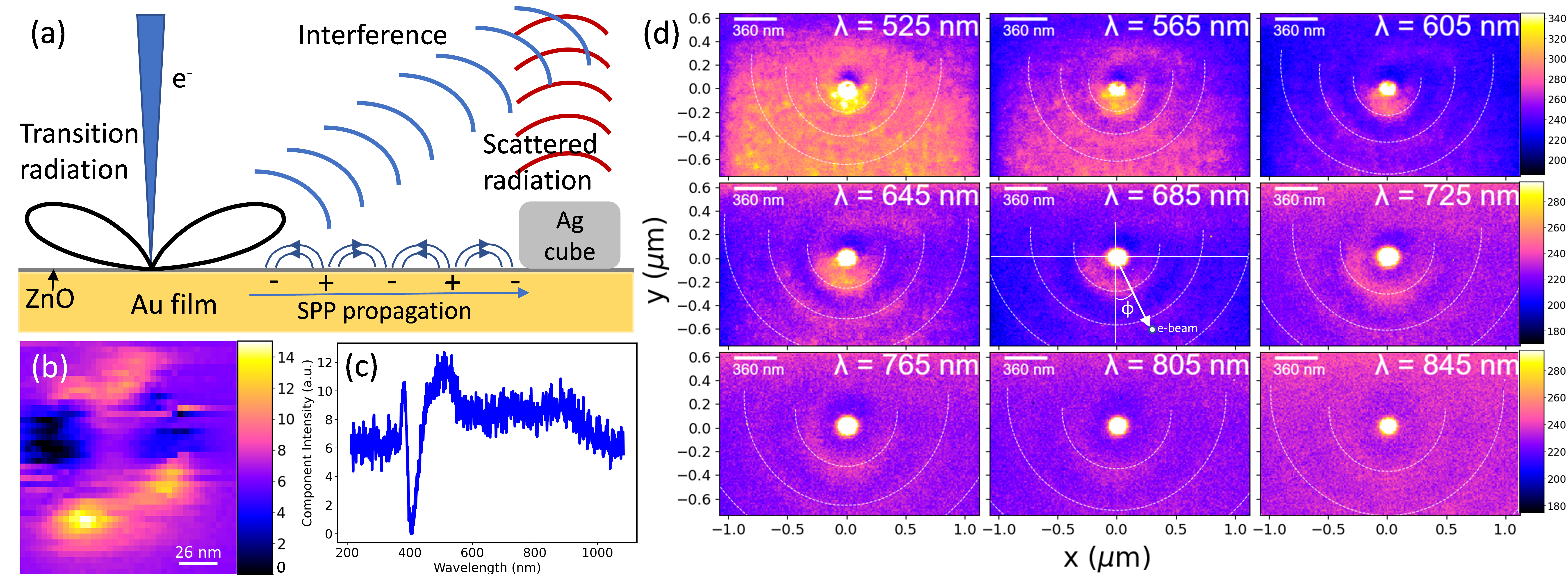
Nanoparticles on metallic planes can act as an antenna to couple free space photons with surface plasmon polaritons (SPPs) Sannomiya et al. 2020. It is crucial to understand this coupling for the current nanopatch antenna system to engineer nanophotonic devices that rely on the out coupling of SPPs to the far field. Notably, the final component of the NMF decomposition shown in Figure 3 (shown in Figures 4 (b) and (c)), is weak compared with the localized modes, and it is very broadband except for an artifact associated with the strong corner modes near 400 nm. It is consistent with broadband SPP modes scattering at the nanocube, but this high resolution image provides no detailed understanding of the SPP propagation on the Au film. Thus, we acquired spectrum images with larger fields of view to characterize interference between transition radiation and SPP CL. This interference allows for near-field imaging of the phase of surface plasmon polaritons before they scatter off the nanocubeKuttge et al. 2009; Hachtel et al. 2019. A clear understanding of SPP propagation combined with the above imaging of nanogap plasmon modes is critical to understanding the composite plasmon-exciton interaction. This understanding is also essential to the ultimate development of dissipative driven entanglement schemes that rely on coupling multiple emitters to shared plasmonic reservoirsDumitrescu and Lawrie 2017; Li, Nemilentsau, and Argyropoulos 2019. Broadband transition radiation is generated when the image-charge-induced dipole in the metal is destroyed as the electron enters the metal. The electron beam also launches SPPs in the metal, which propagate outward. The SPP is scattered into free space photons when it interacts with the nanopatch antenna. A schematic of this process is shown in Figure 4 (a). This scattered radiation has a characteristic phase relative to the transition radiation depending on the distance of the cube from the electron beam. Therefore, the scattered beam and transition radiation can interfere to produce the interferograms shown in Figure 4 (d).
The radial distance which satisfies the interference condition is given by Sannomiya et al. 2020:
| (1) |
where is the phase of the field scattered from the NPA, m is an integer, is the plasmon wave vector that is equal to , where and are the permittivities of ZnO and metal film, respectively, is the azimuthal angle between the NPA and point of electron-beam incidence and is the phase arising due to the distance between the plasmon origin and the NPA. It was previously reported that the phase is zero away from plasmon resonances Sannomiya et al. 2020, and hence due to the high energy of the corner and edge modes ( 520 nm), we set in the wavelength range of 525 to 825 nm, where we observed interference. The parabolic mirror collects all angles from 0 to 90 ∘ and we display the fitting result for as white dashed lines in Figure 4 (d). The thickness of the measured fringes is understood by changing from 0 to 90∘. We plot the calculated fringes for , due to the reduced experimental signal to noise at higher angles. was chosen as , and for the first, second and third interference fringes for all images. Good agreement is obtained between the experimental and theoretical results. This technique can be used for any plasmonic nanoparticle shape to obtain the phase delay and scattering phase.


IV Coupled nanopatch quantum dot heterostructures
While CL microscopy enables clear spectrum imaging of nanogap plasmon modes in these NPAs by using ZnO as spacer layer, the PE layer was moderately deformed by the electron beam during image acquisition. This deformation did not substantially change the optical properties of the nanogap plasmon modes as evidenced by the spectra in Figure 2, but it did modify the morphology of the substrate sufficiently to make drift compensation problematic for long acquisition-time spectrum images. As a result, spectrum images presented in Figure 3 are for the isolated nanocubes on Au film coated silicon substrates with ZnO spacer layers. Below, we compare the CL emission for two different cases where QDs are deposited on a PE spacer layer (on a Au film) with or without nanocubes. We find that in contrast to the PE surface, it is a challenge to adhere the CdSe QDs directly on a ZnO surface (prior to the nanocube deposition). It is also noted that, to date, there has been no careful comparison of the PL and CL of hybrid structures designed to exhibit large Purcell effects.
Point spectra for the CdSe quantum dots dropcast on the PE spacer layer and for the hybrid nanopatch-CdSe quantum dot heterostructure are shown in Figure 5. The data are fit with five Gaussian peaks. The quantum dot contribution to the plasmon-exciton heterostructure is extracted as one of those fit components and plotted separately in the lower panel of Figure 5. Compared with previous reports of quantum dot photoluminescence enhancement by nanogap plasmon modesAkselrod et al. 2016, the cathodoluminescence enhancement compared with the CL of isolated QDs is negligible. This is consistent with a relatively limited literature to date exploring Purcell enhancement of exciton and defect emission by plasmonic heterostructures, where only minimal Purcell enhancement was observed. Feldman et al. 2018; Jiang et al. 2020; Yanagimoto et al. 2020. This is not necessarily surprising, because the electron beam-pumped system exhibits a very different interaction cross-section and different selection rules than the laser-pumped system.
In order to help understand the selection rules associated with electron- and laser-driven plasmon-exciton heterostructures, we acquired complementary optical dark-field (DF) scattering spectra and TRPL spectra in an optical microscope shown in Figures 6(a) and (b) respectively. The DF scattering spectra of several individual NPAs shown in Fig. 6(a) exhibit a small variation in the peak wavelength that is consistent with small variation in the nanocube size or gap thickness. Nevertheless, the NPAs’ peak resonances show an excellent spectral overlap with the QD emission at around 650 nm. Notably, the measured DF scattering under optical excitation exhibits much simpler mode structure than the measured cathodoluminescence because the near-field electron-beam excitation is capable of exciting optically forbidden transitions. Figure 6(b) compares the TRPL of QDs on a glass slide and in an NPA. Similar to the previously observed Purcell enhancement effect in the NPA platform, the decay time of QDs in the NPA is significantly reduced as compared to the intrinsic decay of the same QDs on a glass slideAkselrod et al. 2014; Akselrod et al. 2016; Hoang et al. 2015; Bogdanov et al. 2018. The decay of QDs on a glass slide is well fitted with a single exponential component with a lifetime of 9.5 ns. When the QDs are coupled to the NPA, the decay curve is fitted with a biexponential function deconvolved with the instrument response, resulting in a fast decay component of 0.019 ns and a slower component of 2.19 ns. The fast component is attributed to the decay time of the QDs that are well coupled to the NPA and the slower component is originated from QDs on the Au film, away from the nanocube but within the laser excitation spot. The reduction in the decay of the QDs on a Au film is a result of the nonradiative quenching effect. As it has been shown previously that the decrease in lifetime of the QDs in the NPA is accompanied by a simultaneous increase in the PL intensity Akselrod et al. 2014; Akselrod et al. 2016; Hoang et al. 2015; Bogdanov et al. 2018, the ratio 500 represents the Purcell enhancement factor.
V Conclusion
The TRPL measurements suggest that the heterostructure is well designed with measured Purcell enhancement consistent with the literature, and the samples were transferred in vacuum from the TRPL measurement to the CL measurement, so minimal environmental degradation is expected between measurements. Therefore, the negligible measured Purcell enhancement with electron beam excitation indicates a more fundamental difference between the two measurement modalities. The near-field electron-beam excitation of the NPA excites additional modes than are excited optically, resulting in a broader red-shifted composite NPA response, as shown in Figure 5. Though the QD emission lies within the broadband envelope, the electron beam excitation of modes that are far from resonant with the QD result in substantially reduced plasmon-exciton interactions in the composite system.
However, while it seems clear that CL characterization of hybrid plasmon-exciton heterostructures may not yield the same Purcell enhancement measured in PL spectroscopies, CL microscopy is an indispensable tool for mapping localized and propagating plasmonic modes of technologically relevant nanopatch antenna structures with few nanometer spatial resolution. Further, techniques such as electron-beam induced deposition can be used to pattern plasmonic heterostructures in the SEMWinkler et al. 2017; Iyer et al. 2021 near individual defects or excitons after imaging with CL microscopy, and exert in situ control over plasmon-exciton interactions subject to the understanding that the composite system response will be different under laser excitation than electron beam excitation. Indeed, pump-probe spectroscopies that combine laser and electron beam excitation of the sample should allow for completely integrated experiments that probe the near-field properties of the hybrid heterostructure with an electron beam excitation while probing the resonantly excited state with a laser excitation. Ultimately, this level of integrated manipulation and characterization of hybrid nanophotonic systems is critical to the development of various recently proposed dissipative-driven entanglement schemesDumitrescu and Lawrie 2017; Li, Nemilentsau, and Argyropoulos 2019.
VI Methods
CL microscopy.
CL microscopy was performed in a FEI Quattro environmental scanning electron microscope with a Delmic Sparc cathodoluminescence collection system. A beam energy of 30 keV, and beam currents of 630-5600 pA were used, depending on sample robustness. The sample chamber was maintained at a pressure of 40 Pa water vapor. CL spectra were collected using a parabolic mirror with high numerical aperture of 0.9 and sent to a spectrometer (Andor Kymera 193i) equipped with a 150 line/mm grating and an Andor Newton CCD camera. Spectra were acquired using dwell times of 0.2-2 s per pixel, and spectrum images were acquired by scanning the electron beam while acquiring a CL spectrum at each pixel. Reference images were taken every 2-20 s as necessary during the spectrum image acquisition to allow for drift correction.
Optical characterization. Optical responses of NPA samples were characterized by dark-field scattering and PL measurements through a customized Nikon LV 150N microscope with a 3D nanometer-resolution translation stage (Newport, model 9063). The modified microscope has a halogen lamp for white light illumination and a modified optical path for laser excitation (Coherent laser at 475-nm, 80MHz, 150fs) and PL collection through a bright/dark field 100X microscope objective lens. Dark-field scattering or PL signal from individual NPAs was filtered by a pinhole at a focal imaging plane before entering the spectrometer (Horiba iHR550) and CCD camera (Horiba Jobin-Yvon Synapse). A set of appropriate short-pass (for laser excitation) and long-pass (for PL detection) spectral filters were used for the QD excitation and PL collection. For the decay time measurements of the QDs, a time-correlated single photon counting setup was used. The PL emission from the QDs was collected by the objective lens and sent through the spectrometer for either spectral analysis or through a side exit to be guided into a fast-timing avalanche photodiode for temporal analysis. The signal collected by the photodiode was analyzed by a single photon counting module (PicoHarp 300). Final lifetimes were obtained from fits to the data deconvolved with the instrument response function by using the EasyTau software (PicoQuant).
FEM simulation. Three-dimensional (3D) FEM simulations of the silver (Ag) plasmonic nanopatch antenna structures were performed using Comsol Multiphysics®. The dimensions of the nanocube were identical to the experiments and a spacer layer with thickness of 5 nm was used. The model was surrounded with a spherical scattering boundary condition that prevented backscattering of the electromagnetic waves from the simulation boundaries. A line current was placed vertically 10 nm above the center of the nanocube to simulate the electron beam.Sutter et al. 2021a; Sutter et al. 2021b The induced field plots shown in Figure 3 were obtained by running the simulation twice, once with the line current in vacuum and once with the line current in the presence of the nanopatch antenna, each time using the same mesh. The induced fields were obtained by using the formula: , where is the field calculated with the nanopatch antenna structure and Evac is the field calculated in vacuum. All employed materials were simulated using realistic refractive index data.Stelling et al. 2017; Johnson and Christy 1972
VII acknowledgement
This research was carried out at the Center for Nanophase Materials Sciences (CNMS), which is sponsored at ORNL by the Scientific User Facilities Division, Office of Basic Energy Sciences, U.S. Department of Energy. Support at ORNL for hybrid quantum photonic systems was provided by the U.S. Department of Energy, Office of Science, National Quantum Information Science Research Centers, Quantum Science Center. CA acknowledges support by Office of Naval Research Young Investigator Program (ONR-YIP) under grant no. N00014-19-1-2384. TH acknowledges support from the National Science Foundation (NSF) (Grant no. DMR-1709612).
References
- Wu, Yan, and Lalanne (2021) T. Wu, W. Yan, and P. Lalanne, “Bright plasmons with cubic nanometer mode volumes through mode hybridization,” ACS Photonics 8, 307–314 (2021).
- Baumberg et al. (2019) J. J. Baumberg, J. Aizpurua, M. H. Mikkelsen, and D. R. Smith, “Extreme nanophotonics from ultrathin metallic gaps,” Nature materials 18, 668–678 (2019).
- Maier et al. (2003) S. A. Maier, P. G. Kik, H. A. Atwater, S. Meltzer, E. Harel, B. E. Koel, and A. A. Requicha, “Local detection of electromagnetic energy transport below the diffraction limit in metal nanoparticle plasmon waveguides,” Nature materials 2, 229–232 (2003).
- Maier (2006) S. A. Maier, “Plasmonic field enhancement and sers in the effective mode volume picture,” Optics Express 14, 1957–1964 (2006).
- Brongersma, Hartman, and Atwater (2000) M. L. Brongersma, J. W. Hartman, and H. A. Atwater, “Electromagnetic energy transfer and switching in nanoparticle chain arrays below the diffraction limit,” Physical Review B 62, R16356 (2000).
- Zijlstra, Chon, and Gu (2009) P. Zijlstra, J. W. M. Chon, and M. Gu, “Five-dimensional optical recording mediated by surface plasmons in gold nanorods,” Nature 459, 410–413 (2009).
- Linic, Christopher, and Ingram (2011) S. Linic, P. Christopher, and D. B. Ingram, “Plasmonic-metal nanostructures for efficient conversion of solar to chemical energy,” Nature Materials 10, 911–921 (2011).
- Nie and Emory (1997) S. Nie and S. R. Emory, “Probing single molecules and single nanoparticles by surface-enhanced raman scattering,” Science 275, 1102–1106 (1997), https://science.sciencemag.org/content/275/5303/1102.full.pdf .
- Lee et al. (2021) C. Lee, B. Lawrie, R. Pooser, K.-G. Lee, C. Rockstuhl, and M. Tame, “Quantum plasmonic sensors,” Chemical Reviews 121, 4743–4804 (2021), pMID: 33787252.
- Benz et al. (2016) F. Benz, M. K. Schmidt, A. Dreismann, R. Chikkaraddy, Y. Zhang, A. Demetriadou, C. Carnegie, H. Ohadi, B. de Nijs, R. Esteban, J. Aizpurua, and J. J. Baumberg, “Single-molecule optomechanics in “picocavities”,” Science 354, 726–729 (2016), https://science.sciencemag.org/content/354/6313/726.full.pdf .
- Lawrie et al. (2012) B. J. Lawrie, K.-W. Kim, D. P. Norton, and R. F. Haglund Jr, “Plasmon–exciton hybridization in zno quantum-well al nanodisc heterostructures,” Nano letters 12, 6152–6157 (2012).
- Fofang et al. (2008) N. T. Fofang, T.-H. Park, O. Neumann, N. A. Mirin, P. Nordlander, and N. J. Halas, “Plexcitonic nanoparticles: plasmon- exciton coupling in nanoshell- j-aggregate complexes,” Nano letters 8, 3481–3487 (2008).
- Akselrod et al. (2014) C. Akselrod, Gleb M.and Argyropoulos, T. B. Hoang, C. Ciracì, C. Fang, J. Huang, D. R. Smith, and M. H. Mikkelsen, “Probing the mechanisms of large purcell enhancement in plasmonic nanoantennas,” Nature Photonics 8, 835–840 (2014).
- Akselrod et al. (2016) G. M. Akselrod, M. C. Weidman, Y. Li, C. Argyropoulos, W. A. Tisdale, and M. H. Mikkelsen, “Efficient nanosecond photoluminescence from infrared pbs quantum dots coupled to plasmonic nanoantennas,” ACS Photonics 3, 1741–1746 (2016).
- Huang et al. (2018) J. Huang, G. M. Akselrod, T. Ming, J. Kong, and M. H. Mikkelsen, “Tailored emission spectrum of 2d semiconductors using plasmonic nanocavities,” ACS Photonics 5, 552–558 (2018).
- Cubukcu et al. (2009) E. Cubukcu, S. Zhang, Y.-S. Park, G. Bartal, and X. Zhang, “Split ring resonator sensors for infrared detection of single molecular monolayers,” Applied Physics Letters 95, 043113 (2009).
- Jin and Xu (2006) E. X. Jin and X. Xu, “Plasmonic effects in near-field optical transmission enhancement through a single bowtie-shaped aperture,” Applied Physics B 84, 3–9 (2006).
- Davidson et al. (2016) R. B. Davidson, A. Yanchenko, J. I. Ziegler, S. M. Avanesyan, B. J. Lawrie, and R. F. Haglund Jr, “Ultrafast plasmonic control of second harmonic generation,” ACS Photonics 3, 1477–1481 (2016).
- Pamu et al. (2021) R. Pamu, B. J. Lawrie, B. Khomami, and D. Mukherjee, “Broadband plasmonic photocurrent enhancement from photosystem i assembled with tailored arrays of au and ag nanodisks,” ACS Applied Nano Materials 4, 1209–1219 (2021).
- Jiang et al. (2014) T.-T. Jiang, W.-J. Shao, N.-Q. Yin, L. Liu, J.-L.-Q. Song, L.-X. Zhu, and X.-L. Xu, “Enhanced photoluminescence of CdSe quantum dots by the coupling of ag nanocube and ag film,” Chinese Physics B 23, 086102 (2014).
- Hoang, Akselrod, and Mikkelsen (2016) T. B. Hoang, G. M. Akselrod, and M. H. Mikkelsen, “Ultrafast room-temperature single photon emission from quantum dots coupled to plasmonic nanocavities,” Nano Letters 16, 270–275 (2016).
- Bogdanov et al. (2018) S. I. Bogdanov, M. Y. Shalaginov, A. S. Lagutchev, C.-C. Chiang, D. Shah, A. S. Baburin, I. A. Ryzhikov, I. A. Rodionov, A. V. Kildishev, A. Boltasseva, and V. M. Shalaev, “Ultrabright room-temperature sub-nanosecond emission from single nitrogen-vacancy centers coupled to nanopatch antennas,” Nano Letters 18, 4837–4844 (2018).
- Luo et al. (2018) Y. Luo, G. D. Shepard, J. V. Ardelean, D. A. Rhodes, B. Kim, K. Barmak, J. C. Hone, and S. Strauf, “Deterministic coupling of site-controlled quantum emitters in monolayer wse2 to plasmonic nanocavities,” Nature Nanotechnology 13, 1137–1142 (2018).
- Kleemann et al. (2017) M.-E. Kleemann, R. Chikkaraddy, E. M. Alexeev, D. Kos, C. Carnegie, W. Deacon, A. C. de Pury, C. Große, B. de Nijs, J. Mertens, A. I. Tartakovskii, and J. J. Baumberg, “Strong-coupling of wse2 in ultra-compact plasmonic nanocavities at room temperature,” Nature Communications 8, 1296 (2017).
- Chikkaraddy et al. (2016) R. Chikkaraddy, B. De Nijs, F. Benz, S. J. Barrow, O. A. Scherman, E. Rosta, A. Demetriadou, P. Fox, O. Hess, and J. J. Baumberg, “Single-molecule strong coupling at room temperature in plasmonic nanocavities,” Nature 535, 127–130 (2016).
- Qin et al. (2020) J. Qin, Y.-H. Chen, Z. Zhang, Y. Zhang, R. J. Blaikie, B. Ding, and M. Qiu, “Revealing strong plasmon-exciton coupling between nanogap resonators and two-dimensional semiconductors at ambient conditions,” Physical review letters 124, 063902 (2020).
- Powell et al. (2016) A. W. Powell, D. M. Coles, R. A. Taylor, A. A. R. Watt, H. E. Assender, and J. M. Smith, “Plasmonic gas sensing using nanocube patch antennas,” Advanced Optical Materials 4, 634–642 (2016).
- Xu et al. (2015) D. Xu, S. Yang, Y. Jin, M. Chen, W. Fan, B. Luo, and W. Shi, “Ag-decorated atao3 (a = k, na) nanocube plasmonic photocatalysts with enhanced photocatalytic water-splitting properties,” Langmuir 31, 9694–9699 (2015).
- Lu et al. (2020) W. Lu, Y. Zhang, J. Zhang, and P. Xu, “Reduction of gas co2 to co with high selectivity by ag nanocube-based membrane cathodes in a photoelectrochemical system,” Industrial & Engineering Chemistry Research 59, 5536–5545 (2020).
- Bischak et al. (2017) C. G. Bischak, R. B. Wai, C. Cherqui, J. A. Busche, S. C. Quillin, C. L. Hetherington, Z. Wang, C. D. Aiello, D. G. Schlom, S. Aloni, D. F. Ogletree, D. J. Masiello, and N. S. Ginsberg, “Noninvasive cathodoluminescence-activated nanoimaging of dynamic processes in liquids,” ACS Nano 11, 10583–10590 (2017).
- Hoang and Mikkelsen (2016) T. B. Hoang and M. H. Mikkelsen, “Broad electrical tuning of plasmonic nanoantennas at visible frequencies,” Applied Physics Letters 108, 183107 (2016).
- Hachtel et al. (2019) J. A. Hachtel, S.-Y. Cho, R. B. Davidson, M. A. Feldman, M. F. Chisholm, R. F. Haglund, J. C. Idrobo, S. T. Pantelides, and B. J. Lawrie, “Spatially and spectrally resolved orbital angular momentum interactions in plasmonic vortex generators,” Light: Science & Applications 8, 33 (2019).
- Pakeltis et al. (2021) G. Pakeltis, E. Rotunno, S. Khorassani, D. A. Garfinkel, R. Collette, C. A. West, S. T. Retterer, J. C. Idrobo, D. J. Masiello, and P. D. Rack, “High spatial and energy resolution electron energy loss spectroscopy of the magnetic and electric excitations in plasmonic nanorod oligomers,” Opt. Express 29, 4661–4671 (2021).
- Hachtel et al. (2018) J. A. Hachtel, R. B. Davidson, E. R. Kovalik, S. T. Retterer, A. R. Lupini, R. F. Haglund, B. J. Lawrie, and S. T. Pantelides, “Polarization-and wavelength-resolved near-field imaging of complex plasmonic modes in archimedean nanospirals,” Optics letters 43, 927–930 (2018).
- Feldman et al. (2018) M. A. Feldman, E. F. Dumitrescu, D. Bridges, M. F. Chisholm, R. B. Davidson, P. G. Evans, J. A. Hachtel, A. Hu, R. C. Pooser, R. F. Haglund, and B. J. Lawrie, “Colossal photon bunching in quasiparticle-mediated nanodiamond cathodoluminescence,” Phys. Rev. B 97, 081404 (2018).
- Goris et al. (2014) B. Goris, G. Guzzinati, C. Fernández-López, J. Pérez-Juste, L. M. Liz-Marzán, A. Trügler, U. Hohenester, J. Verbeeck, S. Bals, and G. Van Tendeloo, “Plasmon mapping in au@ag nanocube assemblies,” The Journal of Physical Chemistry C 118, 15356–15362 (2014).
- Konečná et al. (2021) A. Konečná, J. Li, J. H. Edgar, F. de Abajo, and J. A. Hachtel, “Revealing nanoscale confinement effects on hyperbolic phonon polaritons with an electron beam,” arXiv preprint arXiv:2104.01997 (2021).
- Liu et al. (2019) X.-Y. Liu, S. Guo, A. Ramoji, T. Bocklitz, P. Rosch, J. Popp, and H.-Q. Yu, “Spatiotemporal organization of biofilm matrix revealed by confocal raman mapping integrated with non-negative matrix factorization analysis,” Analytical chemistry 92, 707–715 (2019).
- Sannomiya et al. (2020) T. Sannomiya, A. Konečná, T. Matsukata, Z. Thollar, T. Okamoto, F. J. García de Abajo, and N. Yamamoto, “Cathodoluminescence phase extraction of the coupling between nanoparticles and surface plasmon polaritons,” Nano Letters 20, 592–598 (2020).
- Kuttge et al. (2009) M. Kuttge, E. J. R. Vesseur, A. Koenderink, H. Lezec, H. Atwater, F. G. de Abajo, and A. Polman, “Local density of states, spectrum, and far-field interference of surface plasmon polaritons probed by cathodoluminescence,” Physical Review B 79, 113405 (2009).
- Dumitrescu and Lawrie (2017) E. Dumitrescu and B. Lawrie, “Antibunching dynamics of plasmonically mediated entanglement generation,” Physical Review A 96, 053826 (2017).
- Li, Nemilentsau, and Argyropoulos (2019) Y. Li, A. Nemilentsau, and C. Argyropoulos, “Resonance energy transfer and quantum entanglement mediated by epsilon-near-zero and other plasmonic waveguide systems,” Nanoscale 11, 14635–14647 (2019).
- Jiang et al. (2020) M. Jiang, L. Zheng, Y. Li, H. Shan, C. Chi, Z. Liu, Y. Huang, Z. Dang, F. Lin, and Z. Fang, “Tailoring zno spontaneous emission with plasmonic radiative local density of states using cathodoluminescence microscopy,” The Journal of Physical Chemistry C 124, 13886–13893 (2020).
- Yanagimoto et al. (2020) S. Yanagimoto, N. Yamamoto, T. Sannomiya, and K. Akiba, “Purcell effect of nitrogen-vacancy centers in nanodiamond coupled to propagating and localized surface plasmons revealed by photon-correlation cathodoluminescence,” arXiv preprint arXiv:2012.11224 (2020).
- Hoang et al. (2015) T. B. Hoang, G. M. Akselrod, C. Argyropoulos, J. Huang, D. R. Smith, and M. H. Mikkelsen, “Ultrafast spontaneous emission source using plasmonic nanoantennas,” Nature Communications 6, 7788 (2015).
- Winkler et al. (2017) R. Winkler, F.-P. Schmidt, U. Haselmann, J. D. Fowlkes, B. B. Lewis, G. Kothleitner, P. D. Rack, and H. Plank, “Direct-write 3d nanoprinting of plasmonic structures,” ACS applied materials & interfaces 9, 8233–8240 (2017).
- Iyer et al. (2021) V. Iyer, S. T. Retterer, J. Fowlkes, S. Jesse, A. A. Puretzky, J. A. Hachtel, P. D. Rack, and B. J. Lawrie, “In situ electron-beam processing and cathodoluminescence microscopy for quantum nanophotonics,” in Synthesis and Photonics of Nanoscale Materials XVIII, Vol. 11675 (International Society for Optics and Photonics, 2021) p. 1167504.
- Sutter et al. (2021a) P. Sutter, L. K. Khorashad, C. Argyropoulos, and E. Sutter, “Cathodoluminescence of ultrathin twisted ge1–xsnxs van der waals nanoribbon waveguides,” Advanced Materials 33, 2006649 (2021a).
- Sutter et al. (2021b) P. Sutter, J. S. French, L. Khosravi Khorashad, C. Argyropoulos, and E. Sutter, “Optoelectronics and nanophotonics of vapor–liquid–solid grown gase van der waals nanoribbons,” Nano Letters 21, 4335–4342 (2021b).
- Stelling et al. (2017) C. Stelling, C. R. Singh, M. Karg, T. A. F. König, M. Thelakkat, and M. Retsch, “Plasmonic nanomeshes: their ambivalent role as transparent electrodes in organic solar cells,” Scientific Reports 7, 42530 (2017).
- Johnson and Christy (1972) P. B. Johnson and R. W. Christy, “Optical constants of the noble metals,” Phys. Rev. B 6, 4370–4379 (1972).