Tunable electronic and magnetic properties of thin Nb3I8 nanofilms: interplay between strain and thickness
Abstract
The study of novel 2D platforms implementing magnetism in tunable van der Waals (vdW) homo- and hetero-structures paves the way to innovative spintronics and magnetic devices. In this study, we unravel the intriguing properties of few-layer Nb3I8 vdW nanofilms from first principles, showing how and to what extent specific magnetic orderings can be tuned using several degrees of freedom, such as film thickness, stacking geometry, and strain or even a combination of them. All these aspects are explored here, giving a comprehensive view of this novel and promising magnetic material.
Keywords:
van der Waals materials, layer-dependent magnetism, spintronics, straintronicsI Introduction
In the last years, two-dimensional (2D) materials have been attracting tremendous research interest. Their charming properties, induced by the combination of surface effects and quantum confinement, can be exploited to realize 2D platforms-based electronic devices for a wide range of technological applications Liu et al. 2021; Akinwande et al. 2019; Liu et al. 2020. The out-of-plane van der Waals (vdW) interactions allow the integration of deeply different 2D materials, that can thus be viewed as elementary building blocks of new heterostructures showing novel properties and exotic phenomena unavailable in the single-layer constituents. An unprecedented number of degrees of freedom, such as order and number of layers Zhang et al. 2015; Santos et al. 2016; Cantele and Ninno 2017, the twist angle among them Cao et al. 2018; Conte et al. 2019; Lucignano et al. 2019; Cantele et al. 2020, and the distance between two consecutive single layers (interlayer distance) Lebedev et al. 2016; Hu et al. 2016 can be tuned to achieve this goal.
Among these degrees of freedom, strain deserves a special mention, since it offers a viable approach to engineer the electronic, magnetic, and optical properties Cao et al. 2020; Sando et al. 2013; Fei and Yang 2014; Castellanos-Gomez et al. 2013 of 2D nanostructures. The reduced atomic coordination and the enhanced flexibility and elasticity that 2D materials often exhibit when compared with most three-dimensional (3D) crystals Lee et al. 2008; Bertolazzi et al. 2011 have boosted the development of this new field, referred to as “straintronics”.
As far as ground-state magnetism is concerned, several avenues have been devised so far to gain a precise and predictable control over the magnetic states in a number of recently discovered 2D materials. For example, it has been argued that charge doping and/or external strain can significantly affect and modify magnetic phase transitions and exchange interaction Memarzadeh et al. 2021, and are being explored as feasible routes to tune the magnetic ordering in both monolayer ad multilayers systems Jiang et al. 2018; Huang et al. 2018; Li et al. 2019; Song et al. 2019; Wu et al. 2019; Chittari et al. 2020; Tai et al. 2020; Dong et al. 2019.
Since the recent discovery of intrinsic magnetism in monolayers of CrI3 Huang et al. 2017, the exploration of 2D intrinsic magnetic materials has been exponentially increasing Blei et al. 2021. Among the many, we can mention CrI3 and Cr2Ge2Te6 Gong et al. 2017, or those exhibiting high Curie temperature , such as V3I8 Xiao et al. 2019, MnS2 Kan et al. 2014, VSe2 Fuh et al. 2016, and Nb3I8 Conte et al. 2020, all inheriting the magnetic ordering arising from the transition metal -orbitals. In particular, 2D platforms combining ferromagnetism with room and conventional semiconductors open new avenues to implement spintronic applications based on the use of both the charge and the spin degrees of freedom, for example, in next-generation quantum logic chips and nonvolatile magnetic memories with increased densities Žutić et al. 2004; Wolf et al. 2001.
Nb3I8 is a recently synthesized 2D material Oh et al. 2020 with a predicted ferromagnetism at the room temperature ( K) and a layer-dependent magnetism, being ferromagnetic (FM) in monolayer form and antiferromagnetic (AFM) in bilayer and trilayer forms Conte et al. 2020. Also, Nb3I8 monolayer actually is a “ferrovalley” material, because it exhibits an intrinsic spontaneous valley polarization of 107 meV and, thus, the anomalous valley Hall effect without external tunings Peng et al. 2020. All these observations make Nb3I8 an ideal candidate for spintronics and valleytronics applications, as even revealed by recent experimental and theoretical studies Regmi et al. 2022. Nevertheless, a comprehensive explanation of the intriguing electronic and magnetic properties of few-layer Nb3I8 is still missing, so the present work aims to unreveal its potentialities for spintronics applications contributing to the search of novel materials with improved or new functionalities. State-of-the-art first-principles calculations in the framework of density functional theory (DFT) are carried out to bring out the effects of the (in-plane) biaxial strain on the electronic and magnetic properties of Nb3I8 in monolayer, bilayer, and trilayer forms. All these systems are investigated in two different stacking geometries, to establish a possible interplay between thickness, stacking, strain, and magnetism. In particular, we will assess and describe the competition and relative stability between different magnetic phases and the band-gap dependence on the applied strain.
Due to the peculiar nature of Nb3I8, accurate first-principles calculations should definitely take into account two fundamental interactions, that is, vdW interlayer interaction (by an appropriate choice of the exchange-correlation functional) and on-site Coulomb repulsion for Nb 4-electrons (for example, using a DFT+ scheme). Both are carefully included in our analysis, accompanied by a systematic study of the convergence of the presented results with respect to all parameters involved in the calculations. This will be better detailed in the next section.
The paper is organized as follows. In Sec. II we present the computational methods and technical details of our calculations. In Sec. III we show and discuss the electronic and magnetic properties of Nb3I8 films, with special focus on their dependence on the thickness, strain and stacking geometry. Finally, in Sec. IV, we summarize our results and draw some conclusions.
(a) (c)
(c)
(b)

II Methods
All calculations are performed using DFT as implemented in the Quantum-ESPRESSO package (version 6.6) Giannozzi et al. 2009; Giannozzi et al. 2017; Giannozzi et al. 2020. The generalized gradient approximation (GGA) is used with projector-augmented wave (PAW) pseudopotentials Corso 2014 based on the Perdew-Burke-Ernzerhof (PBE) exchange-correlation functional Perdew et al. 1996 to represent the atomic cores PSE. The plane wave basis set is truncated using a cutoff energy of 60 Ry for the plane waves and 480 Ry to represent the charge density in all calculations. An adequate vacuum space of Å is set between periodic replicas along the direction orthogonal to the planes (assumed to be the direction), in order to avoid spurious interactions induced by the periodic boundary conditions. The Brillouin zone (BZ) of the unit cell was sampled using an 881 Monkhorst-Pack -point grid Monkhorst and Pack 1976, grids for supercells were scaled accordingly to guarantee the same accuracy with respect to the -point grid of all calculations. These -point grids have been used for both structural relaxation and total energy calculations.
The vdW interaction has been self-consistently accounted for using the rev-vdW-DF2 Hamada 2014 exchange-correlation functional, that has been proven to be successful in the description of 2D vdW heterostructures with an hexagonal lattice Cantele et al. 2020 and, in particular, provides a good agreement with the available experimental data on Nb3I8 Conte et al. 2020. The supplemental material (SM), in Sec. I, reports typical intralayer binding curves calculated within this approach, characterized by binding energies that are typical of vdW systems.
Based on previous reports Jiang et al. 2017, the on-site Coulomb repulsion of Nb 4 electrons, responsible, as we shall see, of the magnetic behavior of the material, is taken into account by means of the DFT + method Anisimov et al. 1991; Anisimov et al. 1993; Anisimov et al. 1997; Cococcioni and de Gironcoli 2005 with eV. The SM, in Sec. III, contains a number of tests showing that, upon changing within a reasonable range, the reported properties do not exhibit significant variations. In particular, we have verified the stability of the ground-state magnetic ordering, that will be discussed in Sec. III, against . Occupied Kohn-Sham levels do show changes within 0.1-0.2 eV, whereas unoccupied levels shift by much larger energies. This allows to conclude that the main conclusions of the present paper should not be affected by the chosen value of .
The in-plane lattice parameter of all the considered systems has been optimized using spin-polarized calculations. The atomic positions have been fully optimized by means of the Broyden-Fletcher-Goldfarb-Shanno (BFGS) algorithm Broyden 1970; Fletcher 1970; Goldfarb 1970; Shanno 1970, with a convergence threshold of 10-5 Ry on the total energy difference between consecutive structural optimization steps and of 10-4 Ry/Bohr on all components of all the forces acting on the atoms.
In-plane, biaxial strain , where is the optimized in-plane lattice parameter and is the lattice parameter of the strained system, has been applied to the considered structures, ranging from % to 7.5% in steps of 2.5%. Thickness effects have been studied by considering monolayer, bilayer, and trilayer nanofilms, which will be referred to as Nb3I8-L with = 1, 2, 3, respectively.
The effect of the stacking geometry has been assessed for Nb3I8-L and Nb3I8-L, by comparing the bulk stacking, that is the natural order of the layers as they would be arranged in the bulk form, and the AA stacking, constructed by piling different layers with the same planar coordinates.
The ground-state analysis is performed on the non magnetic (NM) and several magnetic states for each system. In particular, since it turns out that Nb3I8-1L has a magnetic ground state with an in-plane FM ordering of the spins, the inter-layer magnetic ordering in thin nanofilms with two or three layers has to be carefully investigated. Indeed, while preserving the in-plane FM ordering, the inter-layer interaction might induce either FM or AFM out-of-plane ordering of the spins, thus giving rise to different spin “stacking sequences”, such as or . This will be better detailed in the next.
Spin-orbit coupling (SOC) has not been included in the calculations, because it does not appear to significantly affect the main conclusions of the paper. An example is shown in Sec. II of the SM, that allows to conclude that the calculated band structures with the inclusion of the SOC do not differ from those calculated in the absence of it.
To conclude this section, it should be pointed out that, mostly as far as the magnetic properties are concerned, accurate convergence tests with respect to the calculation parameters (BZ sampling, plane wave and charge density cut-offs, and so on) are needed. In this respect, we refer to the appendix of Ref. Conte et al. 2020, where a detailed discussion of the convergence of the magnetic stability, band structure, Curie temperature may be found.
III Results and discussion
III.1 Unstrained nanofilms
III.1.1 Bulk Nb3I8
Nb3I8 is a layered transition metal halide belonging to the family of Nb3X8 (X = Cl, Br, I) crystals, having six layers per unit cell (u.c.) in its bulk structure (space group , No. 166) Hulliger 1976. Each single layer shows an I-Nb-I sandwich structure, where the Nb atoms are arranged into an irregular Kagomé lattice formed by triangular Nb3 clusters with side 2.96 Å, separated by a 4.65 Å distance, as sketched in Fig. 1(a). As evidenced in Fig. 1(b), each Nb atom is covalently bonded to a distorted octahedral environment of I atoms, that in turn form a top and a bottom layer that are not equivalent.
III.1.2 Nb3I8-1L
Nb3I8-1L is an intrinsic 2D cluster magnet Conte et al. 2020; Peng et al. 2020, since the magnetic moment per unit cell of 1 is distributed over the Nb3 clusters and results from the seven electrons shared by the Nb atoms. This is depicted in Fig. 1(c), showing the spin polarization isosurfaces in the FM ground state. The NM solution is separated by an energy of 174 meV from the ground state, that protects the magnetic ground state from the thermal fluctuations even at high temperatures. Such a circumstance is supported by the calculations reported in Ref. Conte et al. 2020, where it is shown that such system exhibits a Curie temperature K. The calculated lattice parameter is 7.62 Å and the corresponding band structure is shown in Fig. 2, describing a semiconducting system with a spin-up channel band gap 0.552 eV and a spin-down channel band gap 1.273 eV (highlighted by the shaded orange regions in the figure). It should be pointed out that other and more complex magnetic states, arising in larger (e.g. 22) supercells, can be devised, at an energy from one to few tens of meV higher than the FM ground state Conte et al. 2020. This is an interesting point because, despite the FM state is definitely stable over a wide range of temperatures, phase transitions between different magnetic states could easily occur under suitable conditions (e.g. applied magnetic fields).
The dynamical stability of Nb3I8-1L has been demonstrated both experimentally (isolated monolayers have been successfully obtained onto suitable substrate Kim et al. 2019) and theoretically (from the calculated phonon spectrum, as obtained within the same theoretical framework as that of the present work Jiang et al. 2017). It should be pointed out that, as far as the multilayer and the strained nanofilms considered in the next are concerned, the assessment of the dynamical stability has not be carried out, being computationally quite demanding and out of the scope of the present work. Here, we are going to conceptually support, with the presented results, how the interplay between magnetism, stacking and strain makes Nb3I8 an ideal candidate for novel magnetic devices and functionalities, that certainly demand for further work and investigation.
To conclude the discussion on Nb3I8-1L, the in-plane magnetic coupling, leading to the discussed FM magnetic ordering, can be estimated by building a supercell, as difference between the FM ground state energy and the energy obtained after flipping just one of the spins, out of the four available. The magnetic coupling so obtained is about 23 meV. Such result seems independent on the size of the supercell, since the same value is obtained for a supercell.
III.1.3 Stacking
Starting from Nb3I8-1L, the next layer with bulk stacking is obtained by applying to the former suitable in-plane coordinate transformations. For instance, the second layer results from applying a spatial inversion operation with respect to the center of an Nb3 cluster (inversion center), whereas the third layer results from the first one after applying a suitable fractional translation. On the other hand, multilayer nanofilms with AA stacking can be easily obtained by just replicating the first layer at suitable distances, at fixed in-plane coordinates.
By assuming the (most stable) FM spin ordering within a single layer, the question arises on whether, after stacking two or more layers on top of each other with a given stacking geometry, consecutive layers preferentially carry out the same spin or opposite spins (thus giving rise to a “mixed” spin configuration, with all triangular Nb3 clusters in the same plane exhibiting parallel spins, but with a spin flip when moving form one layer to a nearby one). This is a key concept because the possibility of obtaining a “layered” and eventually tunable (by means of electrostatic doping or out-of-plane pressure) magnetism paves the way to a wide range of applications Jiang et al. 2018; Huang et al. 2018.

III.1.4 Nb3I8-2L
For Nb3I8-2L we explored both bulk and AA stackings, that reveal an in-plane optimized lattice parameter quite similar to that of Nb3I8-1L ( 7.62 Å).
As far as the magnetic ordering is concerned, the most straightforward configuration to be conceived is that of stacking the two layers (with either bulk or AA stacking) with in-plane FM ordering, same as that of Nb3I8-1L (see Fig. 1(c)). In this respect, each layer becomes an “elementary” building block of the multilayer film, carrying a magnetic moment per unit cell (all Nb3 clusters belonging to the same plane carry the same spin). The remaining degree of freedom is that of the relative sign of such moment between the two layers. Therefore, we can conceive two different out-of plane orderings, that will be referred to as FM or (where both layers have a magnetic moment and and the total magnetization is non-zero as well) and AFMz or (where the two layers carry opposite spins, each layer as a non-zero magnetization whereas the total magnetization is zero).
However, aimed at giving a more comprehensive picture of the possible magnetic patterns and their relative stability, supercells were also employed, to explore configurations where each single layer carries a zero total magnetization (two out of the four Nb3 clusters in each plane carry a spin up, the other two a spin down, each plane has a zero magnetization and the total magnetization is zero as well). These configurations will be referred to as AFMxy and are compatibles with different spin patterns, named “stripy-2L”, “Néel-2L”, and “reverted-Néel-2L” states. These patterns, together with FM and AFMz, are sketched in Fig. 3. In the stripy-2L ordering, spin up and spin down in each plane are distributed according to alternating rows, and the same pattern is identically repeated in the two layers. In the Néel-2L ordering spin up and spin down in each plane are distributed according to the supercell diagonal (that is, Nb3 clusters belonging to the same diagonal carry the same spin), and the same pattern is identically repeated on the two layers. Finally, the reverted-Néel-2L state is obtained by flipping the spins of the Néel-2L state in the second layer, such that to a spin-up in the top layer corresponds a spin-down in the bottom layer and the other way around for spin-down. The spin densities associated with the AFMxy orderings are reported in Sec. I of the SM for the sake of completeness.
In the following we report the analysis of the different FM, AFMz and AFMxy magnetic orderings. The relative energy of each magnetic pattern with respect to the lowest-energy AFMz ordering is reported in Tab. 1 for both AA and bulk stacking. The energies are reported per unit cell (u.c.), so as to allow a straightforward comparison between and supercells. It turns out that, regardless of the stacking geometry, the magnetic ground state definitely turns out to be much more stable than the NM solution and that AFMz, among the considered ones, is always the lowest-energy spin pattern . Such circumstance at least partly distinguishes Nb3I8 from CrI3. Indeed, as far as the latter is concerned, while a similar interlayer AFMz ordering has been argued for the bilayer, a stacking-dependent magnetism shows up Xiao et al. 2021; Sivadas et al. 2018; Akram et al. 2021, that seems to lack in Nb3I8. However, in the case of Nb3I8 the stacking geometry plays a role in the relative stability of different magnetic states. Indeed, AFMxy orderings, as depicted in Fig. 3, depending on the stacking, show higher energies, ranging from about 10-20 meV to about 100 meV. On the other hand, the FM state energy is 77 meV/u.c. and 6 meV/u.c. higher than AFMz in the bulk and the AA stacking, respectively. These results reveal that an important role might be played by the deposition steps in the fabrication of real samples, in that the stability of the AFMz ordering against other magnetic orderings gets much more pronounced for bulk stacking. As such, the magnetic phase diagram and its dependence on the temperature can be modified by effect of the stacking geometry.
The effect of the stacking geometry also emerges from the analysis of the spin-polarized band structure. In Fig. 4, the band structure for both AA and bulk stacking is shown for the lowest-energy AFMz state. It can be clearly inferred that for bulk stacking spin-up and spin-down channels provide almost identical band structures (see Fig. 4(b)), with a very tiny difference between the corresponding gaps, eV and eV. This can be ascribed to the inversion symmetry linking the top and the bottom layer in the bulk stacking. On the other hand, for AA stacking, although the overall band structures look similar, the breaking of the inversion symmetry results in a -point dependent spin splitting, yielding the band gaps eV and eV (see Fig. 4(a)). The presence or lack of inversion symmetry for the two stackings can also be easily identified in the charge transfer plots, reported in Sec. I of the SM and showing the ground-state electronic charge difference between Nb3I8-2L and the isolated top and bottom layer.
| Magnetic state | (meV/u.c.) | |
|---|---|---|
| AA stacking | bulk stacking | |
| NM | 292.1 | 103.0 |
| FM () | 5.6 | 76.7 |
| AFMxy-Néel-2L | 21.2 | 96.2 |
| AFMxy-reverted-Néel-2L | 15.6 | 13.7 |
| AFMxy-stripy-2L | 21.2 | 96.2 |
(a)
 (b)
(b)
III.1.5 Nb3I8-3L
At this stage, one might wonder about what would happen if thicker films with an odd number of layers would be considered. Since the AFMz magnetic ordering, corresponding to AFM coupling between two consecutive layers, was proven to be the most stable for Nb3I8-2L, we analyzed similar patterns for Nb3I8-3L. Given the in-plane FM ordering in each layer, different out-of-plane spin-stacking sequences were considered: , analogous of the FM state of Nb3I8-2L; , where neighbor layers carry opposite spin and obtained from the first by flipping the central layer spin; , obtained from the first by flipping the spin of one of the outermost layers. The optimized lattice parameters are 7.63 Å and 7.62 Å for the bulk and the AA stacking, respectively. The ordering, corresponding to AFM coupling between each pair of consecutive layers, has been proven to be the most stable configuration, in agreement with what already reported for trilayer CrI3 Song et al. 2019. In Tab. 2, we report the relative energies per u.c. of all the considered magnetic states with respect to the lowest-energy ordering, for both bulk and AA stacking. Again, the stacking geometry reveals its central role, in that for bulk stacking several tens of meV separate and from the ground state. On the other hand, they lie only 12 and 6 meV from the ground state in the AA stacking.
As far as the ground-state spin-polarized band structure is concerned, we do not expect any degeneracy for both stacking geometries, since no inversion symmetry operation can be identified. Indeed, the bulk stacking shows a semiconducting band structure for both spin channels with eV and eV (see Fig. 5(a)), whereas the AA stacking provides eV and eV (see Fig. 5(b)).
| Magnetic state | (meV/u.c.) | |
|---|---|---|
| AA stacking | bulk stacking | |
| NM | 422.7 | 276.7 |
| 11.9 | 79.5 | |
| 5.9 | 78.0 | |
(a)
 (b)
(b)
As a final remark, we should point out that the out-of-plane AFM magnetic coupling can be estimated, from our results, to be of the order of 6 meV for AA stacking and 80 meV in bulk stacking. Such a coupling is calculated as the the energy needed to flip the spin of a whole layer starting from an otherwise AFMz magnetic configuration and can inferred from both the results for Nb3I8-2L (as in Table 1) and those for Nb3I8-3L (as in Table 2 ). As such, we can conclude that, while the stacking seems not to be able to modify the lowest-energy magnetic configuration, bulk stacking can definitely make it more stable than it is in the AA stacking.
III.2 Strained nanofilms
Applied strain can directly impact on the electronic properties because it affects the interactions between the atoms composing the lattice. In particular, since the magnetism arises from the exchange interactions between the magnetic atoms belonging to the lattice, strain can be devised as an effective degree of freedom for tuning the magnetic couplings and, as a consequence, move the system across the magnetic phase diagram in an absolutely unpredictable way. Here, we analyze in-plane compressive or tensile biaxial strain ranging from % to 7.5% in terms of lattice constant variations and discuss to what extent it can induce magnetic phase transitions.

III.2.1 Nb3I8-1L
Let us start our analysis from Nb3I8-1L. Here, two main questions arise: the first is about whether the strain might stabilize other magnetic phases against the stable FM phase found for the unstrained monolayer. Second, whether and to what extent the electronic properties of a given magnetic phase may change as an effect of the strain.
Aimed at giving an answer to the first question, besides the NM and FM orderings previously discussed for Nb3I8-1L, here we consider also, for the sake of completeness, two other configurations, that is, AFMxy-stripy-1L and AFMxy-Néel-1L (with definitions similar to those of Fig. 3, by keeping in mind that the figure has been conceived for bilayers whereas here we are dealing with a monolayer).
The FM magnetic ordering turns out to be stable against strain effects for all the considered values of tensile and compressive strain. However, larger compressive strain makes the different magnetic states closer in energy to be contrasted with tensile strain that instead further stabilizes the FM state. This can be be easily inferred from Fig. 6, where the relative energy of different magnetic configurations is reported versus the applied strain. This is a striking result because it demonstrates the possibility of using strain as a control knob to stabilize the magnetic phase during the deposition steps, since a sufficiently high tensile (compressive) strain enhances (reduces) the energy difference between NM and FM states and between different magnetic states. The explanation of such behavior requires to remind that, as previously stated, the origin of magnetism in Nb3I8 stands in the irregular Kagomé lattice, where each Nb3 triangular cluster carries a 1 magnetic moment, that is, a 1/2 spin. The magnetic interactions between those clusters are modified by strain, in particular because an enhanced or reduced inter-cluster distance.
Now we turn to the second question, that was about to strain-induced effects on the electronic properties. To this aim, in Fig. 7 the spin-up and spin-down band structures of Nb3I8-1L in the presence of a 7.5% strain are reported. As a general remark, in the strong tensile strain regime, the electronic bands exhibit a flattening deriving from the increased in-plane interatomic distances. A more intriguing effect of the strain on the band structure concerns the band gap variation: by tuning the strain from compressive to tensile, a decrease (increase) of the spin-up (spin-down) channel band gap is observed, as we show in Fig. 7(c). Such an opposite behavior for spin-up and spin-down channel may be ascribed to the number and nature of electronic bands in proximity of the energy gap region. As it will be further clarified in a while from the projection of the energy bands onto atomic orbitals, the relative contribution of I and Nb orbitals to those bands is differently influenced by the strain for the two spins, with a direct effect onto the energy gaps. We could expect that this intriguing peculiarity might be unveiled from absorption experiments, as an example.
(a)
 (b)
(b)
(c)
An in-depth analysis also shows that upon increasing strain a decreasing of the monolayer thickness is observed, ranging from Å for a % strain to Å for a % strain, to be compared with 4.08 Å of the unstrained bilayer (that is indeed intermediate between the other two). In other words, tensile (compressive) strain tends to weaken (enhance) the interatomic interaction along the direction.
As a final remark, we would like to point out that strain-induced effect on the electronic structure can also be related to the change in the orbital hybridization following structural modification. As an example, we report in Fig. 8 the projected density of states (PDOS) onto atomic orbitals. Almost independently of the strain, the top valence bands are mostly dominated by hybridized Nb() and I() orbitals, with the larger contribution coming from the former. However, by looking at an energy window 0.4 eV below the top valence band, the integrated PDOS shows that, on going from the largest compressive strain to the unstrained system to the largest tensile strain the I() contribution to the total PDOS changes from 45% to 32% to 30%, respectively. We can infer that the compressive strain can significantly enhance the hybridization between I and Nb orbitals, whereas the opposite effect is observed in the case of tensile strain.

III.2.2 Nb3I8-2L and Nb3I8-3L
Moving to the thicker nanofilms, in Figs. 9 and 10, the energy differences of different magnetic orderings relative to the lowest-energy state are reported, as a function of the applied strain and for both bulk and AA stackings. It is shown that strain does not significantly alter the ground-state magnetic ordering, in that adjacent layers always carry opposite spin in the lowest-energy state ( for Nb3I8-2L and for Nb3I8-3L).
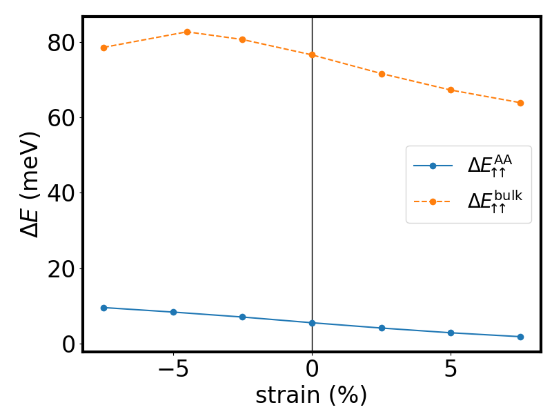

As previously reported for Nb3I8-1L, strain-induced non-trivial modifications of the electronic structure can be observed, in particular as far as spin-up and spin-down band gaps are concerned and more evident for bulk stacking (this is shown in Figs. S2 and S3 of the SM for Nb3I8-2L and Nb3I8-3L, respectively). Moreover, similarly to the Nb3I8-1L, band flattening occurs in the strong tensile strain regime.
IV Conclusions
This work explores the novel and intriguing magnetic and electronic properties of few-layer Nb3I8 vdW nanofilms, showing how and to what extent the magnetism and magnetic ordering can be considered as tunable properties as a function of the film thickness, applied strain, stacking geometry and the combined effect of these three parameters. By considering one-, two-, and three-layer systems, we have shown different magnetic patterns that might be energetically favored among the many possible. Spin densities are shown to be mostly localized on the Nb3 triangular clusters natively present into the irregular Kagomé lattice. In particular, we argued that within each plane a FM ordering is energetically favored, with parallel spins on all Nb atomic sites. In this respect, a single Nb3I8 layer behaves as a “macroscopic” spin carrying a 1 magnetic moment per unit cell. However, as one or more layer are stacked on the first, the inter-layer magnetic interaction drives the system to an out-of-plane AFM ordering of the spins, such that two consecutive layers carry opposite magnetizations. On the other hand, other, both in-plane and out-of-plane magnetic patterns have been shown to be feasible, with energies depending on the stacking geometry and the nanofilm thickness. In particular, the out-of-plane AFM magnetic coupling results more (less) stable in the presence of bulk (AA) stacking, demonstrating how stacking might play a fundamental role for designing new magnetic materials and devices with given functionalities.
Similarly, strain effects have been evidenced, from band flattening taking place for sufficiently large tensile stress, to more dispersed bands with increasing contribution from I orbitals for large modulus compressive stress.
Interestingly, the strain is also capable of enhancing or weakening (according to its sign) the energy differences between different possible magnetic orderings, paving the way to a strain-tunable magnetic response.
The magnetic coupling, responsible for the in-plane FM and the out-of-plane AFM orderings has been estimated from total energy differences. It turns out that it is required an energy of about 23 meV to flip a single spin within a single FM layer. On the other hand, about 6 meV for AA stacking and 80 meV for bulk stacking per unit cell are required to flip the spin of a whole layer starting from two antiferromagnetically coupled layers.
All these results, also combined with recent experimental and theoretical outcomes on the bulk counterpart Regmi et al. 2022, shed light on new and intriguing properties of this novel material, bringing it among the possible candidates to implement more complex magnetic responses, in user-designed homo- and hetero-structures. Our outcomes represent a step forward in the search of thickness-dependent and strain-tunable magnetism in 2D van der Waals materials, which is currently object of intense and ongoing research Ci et al. 2022.
Future work could involve the study of defected Nb3I8 vdW nanofilms, with the aim of bringing out, depending on the defect nature and concentration, the twofold role that might be played, especially in a magnetic system, by the impurities: on one hand, unwanted defects might at least partially destroy the desired (e.g. magnetic) properties. On the other hand, intentionally induced impurities might represent a novel degree of freedom to enhance those properties Cantele et al. 2009; Jiang et al. 2021; Zhao et al. 2021. Moreover, a thorough study of valley polarization and its interplay with strain would be desirable, as being investigated in other classes of two-dimensional materials Zhang et al. 2017; Yang et al. 2019; Guan and Ni 2020.
Acknowledgements.
We acknowledge the CINECA awards HP10CSICON “QUANTERA” and HP10CZRR24 “UNIVERSE” under the ISCRA initiative for the availability of high performance computing resources and support. Financial support and computational resources from MUR, PON “Ricerca e Innovazione 2014-2020”, under Grant No. PIR01_00011 - (I.Bi.S.Co.) are acknowledged.G.C. and F.C. contributed equally to this work.
References
References
- Liu et al. (2021) Y. Liu, X. Duan, H.-J. Shin, S. Park, Y. Huang, and X. Duan, Nature 591, 43 (2021).
- Akinwande et al. (2019) D. Akinwande, C. Huyghebaert, C.-H. Wang, M. I. Serna, S. Goossens, L.-J. Li, H.-S. P. Wong, and F. H. L. Koppens, Nature 573, 507 (2019).
- Liu et al. (2020) C. Liu, H. Chen, S. Wang, Q. Liu, Y.-G. Jiang, D. W. Zhang, M. Liu, and P. Zhou, Nature Nanotechnology 15, 545 (2020).
- Zhang et al. (2015) R. Zhang, B. Li, and J. Yang, Nanoscale 7, 14062 (2015).
- Santos et al. (2016) R. Santos, F. Mota, R. Rivelino, A. Kakanakova-Georgieva, and G. Gueorguiev, Nanotechnology 27, 145601 (2016).
- Cantele and Ninno (2017) G. Cantele and D. Ninno, Phys. Rev. Materials 1, 014002 (2017).
- Cao et al. (2018) Y. Cao, V. Fatemi, A. Demir, S. Fang, S. L. Tomarken, J. Y. Luo, J. D. Sanchez-Yamagishi, K. Watanabe, T. Taniguchi, E. Kaxiras, R. C. Ashoori, and P. Jarillo-Herrero, Nature 556, 80 (2018).
- Conte et al. (2019) F. Conte, D. Ninno, and G. Cantele, Phys. Rev. B 99, 155429 (2019).
- Lucignano et al. (2019) P. Lucignano, D. Alfè, V. Cataudella, D. Ninno, and G. Cantele, Phys. Rev. B 99, 195419 (2019).
- Cantele et al. (2020) G. Cantele, D. Alfè, F. Conte, V. Cataudella, D. Ninno, and P. Lucignano, Phys. Rev. Research 2, 043127 (2020).
- Lebedev et al. (2016) A. V. Lebedev, I. V. Lebedeva, A. A. Knizhnik, and A. M. Popov, RSC Adv. 6, 6423 (2016).
- Hu et al. (2016) Z.-X. Hu, X. Kong, J. Qiao, B. Normand, and W. Ji, Nanoscale 8, 2740 (2016).
- Cao et al. (2020) K. Cao, S. Feng, Y. Han, L. Gao, T. Hue Ly, Z. Xu, and Y. Lu, Nature Communications 11, 284 (2020).
- Sando et al. (2013) D. Sando, A. Agbelele, D. Rahmedov, J. Liu, P. Rovillain, C. Toulouse, I. C. Infante, A. P. Pyatakov, S. Fusil, E. Jacquet, C. Carrétéro, C. Deranlot, S. Lisenkov, D. Wang, J.-M. Le Breton, M. Cazayous, A. Sacuto, J. Juraszek, A. K. Zvezdin, L. Bellaiche, B. Dkhil, A. Barthélémy, and M. Bibes, Nature Materials 12, 641 (2013).
- Fei and Yang (2014) R. Fei and L. Yang, Nano Letters 14, 2884 (2014).
- Castellanos-Gomez et al. (2013) A. Castellanos-Gomez, R. Roldán, E. Cappelluti, M. Buscema, F. Guinea, H. S. J. van der Zant, and G. A. Steele, Nano Letters 13, 5361 (2013).
- Lee et al. (2008) C. Lee, X. Wei, J. W. Kysar, and J. Hone, Science 321, 385 (2008).
- Bertolazzi et al. (2011) S. Bertolazzi, J. Brivio, and A. Kis, ACS Nano 5, 9703 (2011).
- Memarzadeh et al. (2021) S. Memarzadeh, M. R. Roknabadi, M. Modarresi, A. Mogulkoc, and A. N. Rudenko, 2D Materials 8, 035022 (2021).
- Jiang et al. (2018) S. Jiang, L. Li, Z. Wang, K. F. Mak, and J. Shan, Nature Nanotechnology 13, 549 (2018).
- Huang et al. (2018) B. Huang, G. Clark, D. R. Klein, D. MacNeill, E. Navarro-Moratalla, K. L. Seyler, N. Wilson, M. A. McGuire, D. H. Cobden, D. Xiao, W. Yao, P. Jarillo-Herrero, and X. Xu, Nature Nanotechnology 13, 544 (2018).
- Li et al. (2019) T. Li, S. Jiang, N. Sivadas, Z. Wang, Y. Xu, D. Weber, J. E. Goldberger, K. Watanabe, T. Taniguchi, C. J. Fennie, K. Fai Mak, and J. Shan, Nature Materials 18, 1303 (2019).
- Song et al. (2019) T. Song, Z. Fei, M. Yankowitz, Z. Lin, Q. Jiang, K. Hwangbo, Q. Zhang, B. Sun, T. Taniguchi, K. Watanabe, M. A. McGuire, D. Graf, T. Cao, J.-H. Chu, D. H. Cobden, C. R. Dean, D. Xiao, and X. Xu, Nature Materials 18, 1298 (2019).
- Wu et al. (2019) Z. Wu, J. Yu, and S. Yuan, Phys. Chem. Chem. Phys. 21, 7750 (2019).
- Chittari et al. (2020) B. L. Chittari, D. Lee, N. Banerjee, A. H. MacDonald, E. Hwang, and J. Jung, Phys. Rev. B 101, 085415 (2020).
- Tai et al. (2020) B. Tai, W. Wu, X. Feng, Y. Jiao, J. Zhao, Y. Lu, X.-L. Sheng, and S. A. Yang, Phys. Rev. B 102, 224422 (2020).
- Dong et al. (2019) X.-J. Dong, J.-Y. You, B. Gu, and G. Su, Phys. Rev. Applied 12, 014020 (2019).
- Huang et al. (2017) B. Huang, G. Clark, E. Navarro-Moratalla, D. R. Klein, R. Cheng, K. L. Seyler, D. Zhong, E. Schmidgall, M. A. McGuire, D. H. Cobden, W. Yao, D. Xiao, P. Jarillo-Herrero, and X. Xu, Nature 546, 270 (2017).
- Blei et al. (2021) M. Blei, J. L. Lado, Q. Song, D. Dey, O. Erten, V. Pardo, R. Comin, S. Tongay, and A. S. Botana, Applied Physics Reviews 8, 021301 (2021).
- Gong et al. (2017) C. Gong, L. Li, Z. Li, H. Ji, A. Stern, Y. Xia, T. Cao, W. Bao, C. Wang, Y. Wang, Z. Q. Qiu, R. J. Cava, S. G. Louie, J. Xia, and X. Zhang, Nature 546, 265 (2017).
- Xiao et al. (2019) H. Xiao, X. Wang, R. Wang, L. Xu, S. Liang, and C. Yang, Phys. Chem. Chem. Phys. 21, 11731 (2019).
- Kan et al. (2014) M. Kan, S. Adhikari, and Q. Sun, Phys. Chem. Chem. Phys. 16, 4990 (2014).
- Fuh et al. (2016) H.-R. Fuh, C.-R. Chang, Y.-K. Wang, R. F. L. Evans, R. W. Chantrell, and H.-T. Jeng, Scientific Reports 6, 32625 (2016).
- Conte et al. (2020) F. Conte, D. Ninno, and G. Cantele, Phys. Rev. Research 2, 033001 (2020).
- Žutić et al. (2004) I. Žutić, J. Fabian, and S. Das Sarma, Rev. Mod. Phys. 76, 323 (2004).
- Wolf et al. (2001) S. A. Wolf, D. D. Awschalom, R. A. Buhrman, J. M. Daughton, S. von Molnár, M. L. Roukes, A. Y. Chtchelkanova, and D. M. Treger, Science 294, 1488 (2001).
- Oh et al. (2020) S. Oh, K. H. Choi, S. Chae, B. J. Kim, B. J. Jeong, S. H. Lee, J. Jeon, Y. Kim, S. S. Nanda, L. Shi, D. K. Yi, J.-H. Lee, H. K. Yu, and J.-Y. Choi, Journal of Alloys and Compounds 831, 154877 (2020).
- Peng et al. (2020) R. Peng, Y. Ma, X. Xu, Z. He, B. Huang, and Y. Dai, Phys. Rev. B 102, 035412 (2020).
- Regmi et al. (2022) S. Regmi, T. W. Fernando, Y. Zhao, A. P. Sakhya, G. Dhakal, I. B. Elius, H. Vazquez, J. D. Denlinger, J. Yang, J.-H. Chu, X. Xu, T. Cao, and M. Neupane, arXiv , arxiv.2203.10547 (2022).
- Sun et al. (2022) Z. Sun, H. Zhou, C. Wang, S. Kumar, D. Geng, S. Yue, X. Han, Y. Haraguchi, K. Shimada, P. Cheng, L. Chen, Y. Shi, K. Wu, S. Meng, and B. Feng, Nano Letters (2022), 10.1021/acs.nanolett.2c00778.
- Giannozzi et al. (2009) P. Giannozzi, S. Baroni, N. Bonini, M. Calandra, R. Car, C. Cavazzoni, D. Ceresoli, G. L. Chiarotti, M. Cococcioni, I. Dabo, A. D. Corso, S. de Gironcoli, S. Fabris, G. Fratesi, R. Gebauer, U. Gerstmann, C. Gougoussis, A. Kokalj, M. Lazzeri, L. Martin-Samos, N. Marzari, F. Mauri, R. Mazzarello, S. Paolini, A. Pasquarello, L. Paulatto, C. Sbraccia, S. Scandolo, G. Sclauzero, A. P. Seitsonen, A. Smogunov, P. Umari, and R. M. Wentzcovitch, Journal of Physics: Condensed Matter 21, 395502 (2009).
- Giannozzi et al. (2017) P. Giannozzi, O. Andreussi, T. Brumme, O. Bunau, M. B. Nardelli, M. Calandra, R. Car, C. Cavazzoni, D. Ceresoli, M. Cococcioni, N. Colonna, I. Carnimeo, A. D. Corso, S. de Gironcoli, P. Delugas, R. A. DiStasio, A. Ferretti, A. Floris, G. Fratesi, G. Fugallo, R. Gebauer, U. Gerstmann, F. Giustino, T. Gorni, J. Jia, M. Kawamura, H.-Y. Ko, A. Kokalj, E. Küçükbenli, M. Lazzeri, M. Marsili, N. Marzari, F. Mauri, N. L. Nguyen, H.-V. Nguyen, A. O. de-la Roza, L. Paulatto, S. Poncé, D. Rocca, R. Sabatini, B. Santra, M. Schlipf, A. P. Seitsonen, A. Smogunov, I. Timrov, T. Thonhauser, P. Umari, N. Vast, X. Wu, and S. Baroni, Journal of Physics: Condensed Matter 29, 465901 (2017).
- Giannozzi et al. (2020) P. Giannozzi, O. Baseggio, P. Bonfà, D. Brunato, R. Car, I. Carnimeo, C. Cavazzoni, S. de Gironcoli, P. Delugas, F. Ferrari Ruffino, A. Ferretti, N. Marzari, I. Timrov, A. Urru, and S. Baroni, The Journal of Chemical Physics 152, 154105 (2020).
- Corso (2014) A. D. Corso, Computational Materials Science 95, 337 (2014).
- Perdew et al. (1996) J. P. Perdew, K. Burke, and M. Ernzerhof, Phys. Rev. Lett. 77, 3865 (1996).
- (46) We used the scalar relativistic pseudopotentials Nb.pbe-spn-kjpaw_psl.1.0.0.UPF and I.pbe-n-kjpaw_psl.1.0.0.UPF (for Nb and I atoms, respectively) from the Quantum ESPRESSO pseudopotential data base: http://www.quantum-espresso.org/pseudopotentials.
- Monkhorst and Pack (1976) H. J. Monkhorst and J. D. Pack, Phys. Rev. B 13, 5188 (1976).
- Hamada (2014) I. Hamada, Phys. Rev. B 89, 121103(R) (2014).
- Jiang et al. (2017) J. Jiang, Q. Liang, R. Meng, Q. Yang, C. Tan, X. Sun, and X. Chen, Nanoscale 9, 2992 (2017).
- Anisimov et al. (1991) V. I. Anisimov, J. Zaanen, and O. K. Andersen, Phys. Rev. B 44, 943 (1991).
- Anisimov et al. (1993) V. I. Anisimov, I. V. Solovyev, M. A. Korotin, M. T. Czyzyk, and G. A. Sawatzky, Phys. Rev. B 48, 16929 (1993).
- Anisimov et al. (1997) V. I. Anisimov, F. Aryasetiawan, and A. I. Lichtenstein, Journal of Physics: Condensed Matter 9, 767 (1997).
- Cococcioni and de Gironcoli (2005) M. Cococcioni and S. de Gironcoli, Phys. Rev. B 71, 035105 (2005).
- Broyden (1970) C. G. Broyden, IMA Journal of Applied Mathematics 6, 222 (1970).
- Fletcher (1970) R. Fletcher, The Computer Journal 13, 317 (1970).
- Goldfarb (1970) D. Goldfarb, Mathematics of Computation 24, 23 (1970).
- Shanno (1970) D. F. Shanno, Mathematics of Computation 24, 647 (1970).
- Hulliger (1976) F. Hulliger, Structural Chemistry of Layer-Type Phases, edited by F. Lévy, Physics and Chemistry of Materials with A (Springer Netherlands, 1976) p. 392.
- Kim et al. (2019) B. J. Kim, B. J. Jeong, S. Oh, S. Chae, K. H. Choi, S. S. Nanda, T. Nasir, S. H. Lee, K.-W. Kim, H. K. Lim, L. Chi, I. J. Choi, M.-K. Hong, D. K. Yi, H. K. Yu, J.-H. Lee, and J.-Y. Choi, physica status solidi (RRL) – Rapid Research Letters 13, 1800448 (2019).
- Xiao et al. (2021) F. Xiao, K. Chen, and Q. Tong, Phys. Rev. Research 3, 013027 (2021).
- Sivadas et al. (2018) N. Sivadas, S. Okamoto, X. Xu, C. J. Fennie, and D. Xiao, Nano Letters 18, 7658 (2018).
- Akram et al. (2021) M. Akram, H. LaBollita, D. Dey, J. Kapeghian, O. Erten, and A. S. Botana, Nano Letters 21, 6633 (2021).
- Ci et al. (2022) W. Ci, H. Yang, W. Xue, R. Yang, B. Lv, P. Wang, R.-W. Li, and X.-H. Xu, Nano Research (2022), 10.1007/s12274-022-4400-9.
- Cantele et al. (2009) G. Cantele, Y.-S. Lee, D. Ninno, and N. Marzari, Nano Letters 9, 3425 (2009).
- Jiang et al. (2021) X. Jiang, Q. Liu, J. Xing, N. Liu, Y. Guo, Z. Liu, and J. Zhao, Applied Physics Reviews 8, 031305 (2021).
- Zhao et al. (2021) Z. Zhao, W. Li, Y. Zeng, X. Huang, C. Yun, B. Zhang, and Y. Hou, Small Structures 2, 2100077 (2021).
- Zhang et al. (2017) X.-P. Zhang, C. Huang, and M. A. Cazalilla, 2D Materials 4, 024007 (2017).
- Yang et al. (2019) G. Yang, J. Li, Z. Liu, C. Li, and X. Mao, Phys. Chem. Chem. Phys. 21, 15151 (2019).
- Guan and Ni (2020) Z. Guan and S. Ni, ACS Applied Materials & Interfaces 12, 53067 (2020).