Engineering interfacial quantum states and electronic landscapes by molecular nanoarchitectures
Abstract
Surfaces are at the frontier of every known solid. They provide versatile supports for functional nanostructures and mediate essential physicochemical processes. Being intimately related with two-dimensional materials, interfaces and atomically thin films often feature distinct electronic states with respect to the bulk, which are key for many relevant properties, such as catalytic activity, interfacial charge-transfer, or crystal growth mechanisms. Of particular interest is reducing the surface electrons’ dimensionality and spread with atomic precision, to induce novel quantum properties via lateral scattering and confinement. Both atomic manipulation and supramolecular principles provide access to custom-designed molecular superlattices, which tailor the surface electronic landscape and influence fundamental chemical and physical properties at the nanoscale. Herein, we review the confinement of surface state electrons focusing on their interaction with molecule-based scaffolds created by molecular manipulation and self-assembly protocols under ultrahigh vacuum conditions. Starting from the quasi-free two-dimensional electron gas present at the (111)-terminated surface planes of noble metals, we illustrate the enhanced molecule-based structural complexity and versatility compared to simple atoms. We survey low-dimensional confining structures in the form of artificial lattices, molecular nanogratings or quantum dot arrays, which are constructed upon appropriate choice of their building constituents. Whenever the realized (metal-)organic networks exhibit long-range order, modified surface band structures with characteristic features emerge, revealing intriguing physical properties, such as discretization, quantum coupling or energy and effective mass renormalization. Such collective electronic states can be additionally modified by positioning guest species at the voids of open nanoarchitectures. The necessary insight into these scattering potential landscapes can be obtained through semiempirical models, which brings closer the prospect of total control over surface electron confinement and quantum engineering.
I 0. Introduction
Reaching atomistic control and understanding of matter has been a long-nourished desire of mankind, receiving widespread attention once the foundations of atomic and molecular sciences were established. Enormous efforts were dedicated to develop fabrication, characterization, and manipulation procedures providing access to novel expressions of materials, useful electronic, photonic and magnetic properties, or collective atomic states with ever increasing precision and complexity Klitzing et al. 1980; Shechtman et al. 1984; Amano et al. 1986; Heeger et al. 1988; Binasch et al. 1989; Davis et al. 1995; Kane and Mele 2005; Bloch et al. 2008; Mühlbauer et al. 2009.
Multiple instrumental developments were crucial to grant direct insights into the nature and behaviour of atomic and molecular species down to the Ångström regime, whereby the imaging capabilities by electron, field-ion, scanning tunneling microscopy (EM, FIM, STM) techniques proved to be extremely valuable.
Striking direct visualization of crystal surface atomic lattices and adsorbed species could be firstly achieved by FIM and later on with the more versatile STM, generating not only revolutionary scientific insights but also inspiration and opportunities for generations of researchers Müller 1965; Binnig and Rohrer 1987.
Using cryogenic STM the paradigmatic advance of addressing and positioning individual atoms became a reality Stroscio and Eigler 1991 and was immediately recognized as an emblematic achievement in nanoscale science.
Likewise, insights into the essential electronic structure of materials became accessible by means of local scanning tunneling spectroscopy (STS) and space-averaging high-resolution spectroscopies, notably including angle-resolved photoemission (ARPES) Damascelli et al. 2003. The combination of these powerful tools, ideally complemented with theoretical modeling is an asset to fully characterize electronic properties and their implications. Lobo-Checa et al. 2009; Gambardella et al. 2003; Klappenberger 2014; Galeotti et al. 2020; Yin et al. 2021.
Bottom-up construction procedures were developed to design a wide variety of nanosystems amenable to scanning probe and space-averaging scrutiny. In particular, since the turn of this century, supramolecular chemistry principles have been increasingly employed to create low-dimensional functional nanostructures at well-defined interfaces Barth et al. 2000; Theobald et al. 2003; Yokoyama et al. 2001; Stepanow et al. 2004. They are readily achieved by selecting appropriate molecular species with defined endgroups favoring self-assembly into purely organic or metal-organic nanoarchitectures Barth et al. 2005; Kühnle 2009; Kudernac et al. 2009; Dong et al. 2016a; Goronzy et al. 2018; Xing et al. 2019. In this context, supramolecular nanoporous networks were utilized as host lattices for the preferential trapping of guest species or as confining arrays for molecular motion Theobald et al. 2003; Stöhr et al. 2007; Kühne et al. 2010; Pivetta et al. 2013; Nowakowska et al. 2016; Zhang et al. 2015; Nowakowska et al. 2015; Teyssandier et al. 2016. Moreover, they provide significant potential for incorporation of molecular switches in nanoelectronic circuits Kocić et al. 2019 or to host ligands suitable for gas sensing applications Gutzler et al. 2015; ˇ
C
echal
et al. 2016; Écija et al. 2018. In addition, metal-organic networks are appealing for the exploration of novel magnetic properties Umbach et al. 2012; Abdurakhmanova
et al. 2013; Gao et al. 2020, catalytic effects Gutzler et al. 2015; ˇ
C
echal
et al. 2016; Hötger et al. 2019, oxidation states Li et al. 2012, and exotic tessellation patterns (e.g., quasicrystals or Archimedean tilings) Urgel et al. 2016a; Zhang et al. 2018; Yan et al. 2017, with the added prospect of exhibiting tunable quantum phases and topological properties Zhang et al. 2016a; Kumar et al. 2018; Gao et al. 2019; Sun et al. 2018; Dong et al. 2016b; Wang et al. 2013a; Hernández-López
et al. 2021; Jiang et al. 2021.
The extensive activities devoted to the exploration of quantum confinement and quasiparticle scattering at nanostructures on metal surfaces promoted the advance of condensed matter research. This progress is revisited here taking the surface states of coinage metals as a canonical playground, whereby the design of appropriate nanoarchitectures tailors the electronic structure and topology of the outermost layers. We also introduce the generally relevant aspects underpinning the scattering and confinement phenomena of two-dimensional electron gases (2DEGs) existing at appropriate surfaces listing prominent cases where exquisite control over such 2DEGs is exerted.
We cover the ground-breaking quantum corral and resonator structures built by atomic manipulation and move into more complex molecule-based arrangements and supramolecular self-assemblies. The latter enable an upscaling of the quantum properties due to the mesoscopic templating, which is a requirement for (opto-)electronic devices manufacturing. The electronic structure of these systems is explored mainly by two complementary experimental techniques: STM/STS at the atomic level, and ARPES whenever large and homogenous domains exist. Semiempirical methods are recurrently used to simulate the molecular scattering potential landscape responsible for such 2DEG modification.
Moreover, we discuss electronic structure modifications by artificial lattices yielding exotic properties such as Dirac cones or flat bands Gomes et al. 2012; Slot et al. 2017, topological edge states Kempkes
et al. 2019a; Freeney
et al. 2020a, fractal behaviour Kempkes
et al. 2019b or Penrose tiling quasicrystals Collins et al. 2017, which are at the foundation of emerging fields such as twistronics Cao et al. 2018a; Cao et al. 2018b and mirror concepts established for Bose-Einstein condensates Ketterle 2002; Zapf et al. 2014; Park and Louie 2009a; Polini et al. 2013; Leykam et al. 2018; Greiner et al. 2002. Such emerging properties often exist for natural materials, such as graphene, but are here induced, and importantly, tuned by the proper nanostructuring of the featureless dispersion of the 2DEGs at metal surfaces.

II I. Harnessing surface states to explore quantum mechanical phenomena
Well-defined surfaces offer a plethora of intriguing properties and have been studied extensively for more than a century. With the development of ultrahigh-vacuum technology, systematic investigations of the surface atomic arrangement and electronic structure became possible Duke 2003. In later years, atomistically clean metal surfaces served as versatile platforms for the construction of precisely defined nanoscale architectures, the dimension of which falls below the wavelength of Fermi electrons whence the quantum regime is entered. Electron scattering with confining attributes on surfaces emerge at natural defects or reconstructions, as well as nanostructures realized by STM tip manipulation Gross et al. 2004; Pennec et al. 2007; Klappenberger et al. 2009; Lobo-Checa et al. 2009; Cheng et al. 2010; Wang et al. 2013b; Müller et al. 2016; Martín-Jiménez
et al. 2019.
As illustrated in Figure 1, lowering the spatial dimensions has a conspicuous effect on the density of states (DOS) of a free-electron gas system Ashcroft and Mermin 1976. The smooth three dimensional (3D) DOS distribution (E1/2) evolves into energy-independent step-like staircases in two-dimensions (2D) and reaches fully discretized “delta function” [(-)] lineshapes in zero-dimensional (0D) systems, while in one-dimensional (1D) structures a convolution of the previous distributions is found.
The relevance of DOS modification upon dimensional reduction in electronic systems can be gauged from its extended application in the semiconductor industry that relies on ultrathin, quasi-2D electron systems for building electronic and computational devices Brennan 1999; Yoffe 2001; Zwanenburg et al. 2013; van Wees et al. 1988; Kanisawa et al. 2001. Even future quantum computation realization may come in reach using tailored low-dimensional superconducting structures Sato and Ando 2017; Nayak et al. 2008; Choi et al. 2019.
Because high-technology developments were stimulated by the fabrication of quantum wire (QW) and quantum dot (QD) architectures, understanding the plethora of fundamental properties of low-dimensional systems is important to explore new applications fields Barth et al. 2005; Harrison 2005; van der Wiel et al. 2002; Hanson et al. 2007; Pekola et al. 2013; Wharam et al. 1988; Ohnishi et al. 1998; Tarucha et al. 1996. Particularly, material engineering, molecular electronics, and quantum computation require the construction and exploration of artificial coupled or hybrid quantum materials Kagan and Murray 2015; Kagan et al. 2016; Broome et al. 2018; Leon et al. 2020; Walkup et al. 2020; Tokura et al. 2017; Keimer and Moore 2017. Possible candidates may emerge from 2D materials that exhibit long-range magnetic order Huang et al. 2017; Gong et al. 2017, flat bands or low-temperature superconductivity Cao et al. 2018a; Cao et al. 2018b; Andrei and MacDonald 2020; Kezilebieke et al. 2020; Li et al. 2021, providing an outstanding platform to obtain distinct quantum states of matter.

II.1 A. Surface states providing canonical 2DEGs
The model systems chosen in this review to address the scattering and confinement properties of diverse artificial or self-assembled nanostructures are the well-known Shockley states present at the (111)-terminated coinage metal surfaces (Cu, Ag and Au) Shockley 1939. These 2D surface states exist in the -L projected bulk band gap Kevan and Gaylord 1987; Paniago
et al. 1995a. The pertaining electrons, principally residing at the outermost surface layers, behave as a quasi-free 2DEG, propagating unrestricted (with plane wave characteristics) in a regular and pristine surface plane Reinert et al. 2001; Reinert and Hüfner 2005; Malterre et al. 2007; Oka et al. 2014; Tamai et al. 2013 [Fig. 2(a)]. Their quasi-free character is mirrored in the parabolic dispersion [see Fig. 2(b-d)] Reinert et al. 2001; Paniago
et al. 1995b that follows the relation =+, where is the fundamental binding energy of the surface state (, the band minimum), the electron’s effective mass, and the wave-vector parallel to the surface (cf. Table 1). Energy and wave-vector can be directly probed using ARPES that can nowadays access the spin-orbit splitting, encountered for instance for Au(111) LaShell et al. 1996; Tamai et al. 2013 and even their proposed topological properties in combination with two-photon photoemission (2PPE) Yan et al. 2015.
The isotropic dispersion of these Shockley states results in step-like DOS distributions characteristic for 2D systems (Figure 1). The relating electronic characteristics can be directly accessed at the atomic (local) scale by scanning tunneling spectroscopy (STS) using differential conductance spectra (s) Tersoff and Hamann 1985 [see Fig. 2(a)]. The observed local density of states (LDOS) correlates with the spatially integrated ARPES signals since the STS onset of the Shockley states matches the band bottom (fundamental) energies of these low-dimensional systems [cf. Fig. 2(a) and (d)].
| [meV] | / | [Å-1] | [Å] | |
|---|---|---|---|---|
| Ag(111) | 631 | 0.397 | 0.080 | 78.5 |
| Au(111) | 4871 | 0.255 | 0.167/0.192 | 32.7/37.6 |
| Cu(111) | 4351 | 0.412 | 0.215 | 29.2 |

Metal surface 2DEGs reside at the outermost atomic planes and are therefore very sensitive to impurities in the form of adsorbed atoms or molecules Bertel and Memmel 1996; Kulawik et al. 2005, structural defects such as atomic steps or vacancy islands Crommie
et al. 1993a; Hasegawa and Avouris 1993; Li et al. 1999; Rodary et al. 2007; Avouris and Lyo 1994; Bürgi et al. 1998 and thin overlayers comprising e.g., rare gases or alkali metals Forster et al. 2004. In STM topographic data these effects become manifest and can be directly resolved when applying small bias voltages at low temperatures, whereby Fermi level electrons dominate the tunneling current [Fig. 3(a, b)]. The pertaining electron density oscillations exhibit standing wave character and are related to Friedel oscillations generated by point-like charge impurities in bulk systems Friedel 1958, that can be rather pronounced, depending on material characteristics Sprunger et al. 1997.
Such standing wave oscillations are recognized as quasiparticle interference (QPI) patterns, originating from the constructive interference of electron waves after scattering at surface obstacles. Importantly, when Fourier transforming the QPI patterns taken at different bias voltages, the full energy and momentum space (band dispersion) of these electrons can be accessed. Similar to single atoms, molecular adsorbates equally scatter interfacial 2DEGs and produce QPI patterns. In large molecular species typically a repulsive potential is generated by the charge distribution through the molecular backbone. Remarkably, as shown for isolated species, not all molecular moieties necessarily scatter in the same way Gross et al. 2004 [cf. Fig. 3(c)]. It also must be mentioned that surface-state-mediated interactions exist, which can influence the spatial distribution of adsorbates at surfaces Repp et al. 2000; Knorr et al. 2002; Ternes et al. 2010. Under suitable conditions these adatoms are placed at positions reflecting an oscillatory interaction arising due the surface state electrons, with periodicity and 1/ decay, whereby turns out to be the distance between neighboring adatoms Han and Weiss 2012; Ding et al. 2007; Knorr et al. 2002; Repp et al. 2000; Silly et al. 2004. These indirect interactions are also the driving force for the creation of superlattices of individual adsorbed atoms when the adatom concentration, the sample temperature and the adatom diffusion barrier are in subtle balance [Fig. 4(a)].

II.2 B. Principles of 2DEG confinement by atomic steps, corrals and superlattices
To systematically engineer and confine freely propagating surface electrons it is neccessary to reduce the system’s dimensionality to one or zero dimensions by building QW or QD structures. Since adsorbed atoms and vacancies Crommie
et al. 1993a; Crommie
et al. 1995a; Kliewer et al. 2001; Li et al. 1998; Li et al. 1999; Jensen et al. 2005, molecules Gross et al. 2004; Shchyrba
et al. 2014a and step edges Bürgi et al. 1998; Hasegawa and Avouris 1993; Avouris and Lyo 1994 efficiently scatter the surface electrons, three approaches were established to produce well-defined 2DEG confining nanostructures that are schematically reproduced in Fig. 5: (a) step arrays and nanogratings, (b) discrete artificial nanostructures via atomic or molecular manipulation, and (c) self-assembled atomic superlattices and molecular nanoporous networks. 1D-QWs in the form of step arrays and nanogratings confine the surface electrons in the ’horizontal’ direction by periodically spaced scattering barriers, whereas, except for an energy shift, a free-electron behavior is kept perpendicular to it (in the ’vertical’ direction) [Fig. 5(a)]. More restrictive are QDs that confine the electrons in all directions. In particular, QD superlattices emerge whenever the confinement occurs on the surface from point-like (0D) scattering units periodically distributed in the nanoscale regime [Fig. 5(b)]. These scattering superlattices are often realized artificially via atomic or molecular manipulation, but also by self-assembly. A very promising engineering approach to obtain coupled QDs exploits the spontaneous self-assembly of simple organic building blocks on surfaces. Thus molecular nanoporous networks can be fabricated being purely organic or comprising metal-organic coordination motifs [Fig. 5(c)]. Note that the embedded metal centers and the molecules may scatter surface electrons differently, whence an interesting heterogenous scattering potential landscape for the 2DEG confinement and QD intercoupling emerges, the consequence of which will be explained later in section IV. Until the end of this section, we summarize relevant cases of QW and QD systems built from inorganic materials.


1D electronic states spontaneously evolve on noble metal surfaces whenever parallel steps define single terraces [Fig. 6(a)]. Alternatively, they can be created artificially by arranging adspecies into parallel atomic wires [Fig. 6(d)]. The atomic steps efficiently back-scatter the surface electrons [see Fig.2 (a)], producing confined states –commonly known as lateral quantum well states (QWS)– when the average terrace width falls below the surface state electron coherence length Bürgi et al. 1998; Oka et al. 2014 [Fig. 6(a)]. These QWS can be modeled using infinite confining potential barriers at steps Bürgi et al. 1998; Ortega et al. 2013, so that electron motion becomes restricted within the terrace with freedom to travel parallel to the steps Ortega et al. 2018 (analogous to Fabry-Pérot resonators known from optics). As observed in Fig. 6(b), the energy of such QWS can be tuned by altering the terrace width or the atomic-row spacing Negulyaev et al. 2008; Fernández et al. 2016.
This scenario becomes even more intriguing whenever a periodic (regular) step array is created on the surface, going beyond two parallel steps or a set of terraces with different widths. Such regular vicinal crystals Mugarza et al. 2006; Baumberger et al. 2002; Baumberger et al. 2004; Shiraki et al. 2004 provide step superlattices giving rise to extended quasi-1D band structures that can be probed by non-local techniques such as ARPES. The electron confinement within the terraces leads to gapped and anisotropic dispersions accomplished by upward shifts of the 2DEG fundamental energy scaling inversely with the terrace size. Importantly, some electronic coupling between adjacent terraces emerges, which translates into finite step potential barriers that have to be taken into account Mugarza et al. 2006; Ortega et al. 2013; Mitsuoka and Tamura 2011. The physical nature of the modulated electronic bands can be captured by the 1D-Kronig Penney model Mugarza et al. 2006. Herein, the steps are considered repulsive, in the form of square-shaped finite potential barriers of magnitude , where corresponds to the height of the barrier and to its width Ortega et al. 2011.
A beautiful example of the resulting quasi-1D band structure is shown in Fig. 6 (c) for the case of Au(23 23 21) featuring a miscut angle of ∘ from the (111) plane Mugarza and Ortega 2003. By analysing the energy distribution curves (EDCs), weakly dispersive peaks separated by energy gaps are observed in the direction perpendicular to the steps, whereas the parallel direction exhibits the expected (unconfined) parabolic dispersion Mugarza and Ortega 2003.

Nanostructures enclosing specific areas provide striking electron confining properties (Fig. 7). Atomic arrangements constructed by tip manipulation methods were introduced as “quantum corrals” Crommie
et al. 1993b; Heller et al. 1994; Crommie
et al. 1995a; Crommie
et al. 1995b; Kliewer et al. 2001 that exhibit distinct standing wave patterns, i.e., QPI phenomena clearly revealing the 2DEG response to the confining geometries (e.g., hexagons, circles, squares or triangles) Braun and Rieder 2002; Lagoute et al. 2005; Kumagai and Tamura 2008; Kliewer et al. 2001. For some cases, the confining properties are almost element-independent, whence different adatom species (e.g. Fe and Mn) result in similar STS signatures [Fig. 7(a), (b)] Crampin and Bryant 1996. Moreover, at the corral center the DOS may feature a multipeak lineshape, stemming from confined resonances drifting apart as the enclosed area is reduced.
The adatoms defining the quantum corrals can be modelled as an impenetrable boundary, i.e., a hard-wall barrier and thus, the eigenstates and the eigenenergies can be determined using a particle in a 2D box model of the corresponding geometry Heller et al. 1994; Kumagai and Tamura 2008; Kumagai and Tamura 2009; Tatsumi et al. 2018. However, experimentally finite peakwidths (more evident as the energy separates from the 2DEG onset) are detected instead of delta functions expected for perfectly isolated quantum boxes. Thus, the nanostructure walls require the consideration of leaky barriers that reflect only a fraction of the incident amplitude Heller et al. 1994; Crommie
et al. 1995b; Kliewer et al. 2001; Harbury and Porod 1996; Rahachou and Zozoulenko 2004; Fiete and Heller 2003. The existence of inelastic absorptive channels has been ascribed to the coupling of surface electrons with bulk states Crommie
et al. 1995a; Fiete and Heller 2003; Kliewer et al. 2001. To avoid specific assumptions or empirical input data, ab initio calculations based on density functional theory and a multiple scattering approach employing the Korringa-Kohn-Rostocker Green’s function method were used to describe the electronic structure of quantum corrals Niebergall et al. 2006. Alternatively, the elastic scattering theory approach (finite-height potential barriers) turned out to be a simpler model capable of reliably reproducing the experimental findings Harbury and Porod 1996; Rahachou and Zozoulenko 2004. Furthermore, similar LDOS distributions to those encountered for quantum corrals were found in nanovacancies or adatom islands created by gentle sputtering on Ag(111), i.e., without involving direct atom manipulation Li et al. 1998; Li et al. 1999; Jensen et al. 2005; Crampin et al. 2005 [see Fig. 7(c)].
The surface-state-mediated superlattices also exhibit 0D partial confinement of the 2DEG. An example is the case of Ce adatoms on Ag(111), where the atoms arrange in perfectly ordered triangular QD units, the size of which can be altered with careful coverage control Silly et al. 2004; Ternes et al. 2004; Ternes et al. 2010 [Fig. 4(a)]. With increasing Ce concentration, the position of the first confined state shifts quadratically to higher energies with the average distance , as shown in Fig. 4(b). Note that the Ag surface state becomes depopulated in these cases and appears in the unoccupied regime ( ), where resonances in the form of LDOS peaks appear. Moreover, not only ordered superlattices can confine the 2DEG, but also disordered ones. In this regard, researchers succeeded in generating and probing wavefunctions of a disordered 2DEG multifractal scaling characteristics, using the mixed surface alloy BiPb/Ag(111) Jäck et al. 2021.
The quantum corrals can also be regarded as artificial atoms, in view of their discrete electronic levels. In recent work their bonding properties were explored using atomic force microscopy. The measured interactions are very weak, but covalent attraction to metallic and repulsions for CO terminated tips could be discriminated. Stilp et al. 2021.

It is possible to go beyond the “standard” electronic confinement control by constructing specially configured quantum corrals enclosing magnetic impurities. For instance, the so-called quantum mirage gives rise to remarkable nanomagnetic effects by positioning a single Co adatom at one focus of an ellipsoidal quantum corral Manoharan et al. 2000; Stepanyuk et al. 2005 [Fig. 8(a)]. The Co atom Kondo signature becomes replicated (with reduced intensity) at the second, pristine (Co-free) focal point. Therefore, the corral acts as a quantum mechanical resonator and the 2D confined Cu surface state electrons form the medium through which the magnetic moment of the Co adatom is projected to the opposite focus Stepanyuk et al. 2005; Rossi and Morr 2006; Figgins et al. 2019. Recently the Kondo-free mirage effect was also demonstrated using Fe and Ag single atoms Li et al. 2020a. Overall, the quantum size effects in corrals or nanoislands promote important effects, such as the observation of quantum-guided diffusion and adatom self-assembly, the control of statistical fluctuations, the tunability of the Kondo temperatures or the build up of atomic logic gates Li et al. 2020b.
Likewise, adsorbed magnetic clusters provide additional magnetic effects triggered by confinement. For example, triangular 2 ML thick Co islands on Cu(111) not only display efficient confinement of the Cu 2DEG, but also spin-dependent quantum interference effects [Fig. 8(b)]. Differential tunneling conductance () asymmetry maps show strong position-dependent signals within the Co islands. A rim state localized at the edges (in blue) originates from minority states, while the modulation pattern at the inner part (in red) shows the opposite (majority) spin character, which is ascribed to the electron quantum confinement of the free electron-like surface state (i.e., the Cu 2DEG) Oka et al. 2010; Pietzsch et al. 2006; Oka et al. 2014. A similar spin-confinement interplay effect has been demonstrated from the analysis of QPI phenomena on Bi(110), where spin-orbit interactions entail a marked surface state splitting, emphasizing that their spin character cannot be neglected Pascual et al. 2004.
Over recent years, 2DEG scattering and confinement were examined for a series of prototypical topological insulator materials exhibiting insulating bulk and topologically protected spin-split surface states Zhang et al. 2020a; Sobota et al. 2021. Due to their intriguing quantum nature, remarkable effects in striking contrast to the previous scenarios described occur in these materials, as for example the transmission through steps Seo et al. 2010. Moreover, an analysis of confinement patterns for the scattering of topological states from Ag impurities and step edges on the Bi2Te3(111) surface indicated a complete suppression of electron backscattering, due to the manifestation of time-reversal symmetry Zhang et al. 2009. However, more recent studies on such substrates featuring triangularly shaped Bi quantum corrals atop displayed quasi-bound states, indicative of topological surface state confinement effects Chen et al. 2019. Based on these findings, selection rules were suggested, governed by the shape and spin texture of the surface state constant energy contour upon the strong hexagonal warping in the substrate Zhang et al. 2020a; Sobota et al. 2021. In more recent work, even the dual (weak-crystalline) topological material Bi2TeI was spectroscopically investigated, displaying distinct 2D Dirac surface states behaving differently in the vicinity of atomic steps and susceptible to mirror symmetry breaking Avraham et al. 2020. Related to these findings is the demonstration of spin-polarized midgap states at odd atomic step edges of stoichiometrically controlled PbSnSe alloys featuring topological crystalline insulator surfaces Sessi et al. 2016. Interestingly, also the Shockley states of Au(111) and other noble metals can be interpreted as topologically derived surface states of a topological insulator Yan et al. 2015.
A remarkable effect in the noble metal surface states is that they can be made superconducting by the proximity effect Potter and Lee 2012; Wei et al. 2019. Using a hybrid material platform consisting of a thin Au(111) film on superconducting vanadium substrate and patterned EuS, to additionally magnetize the surface state electrons via exchange coupling, the signatures of so-called Majorana zero modes could be accessed Manna et al. 2020.
In the following we focus on the electronic confinement and scattering properties induced by molecular nanoarchitectures fabricated on (111)-terminated metals featuring Shockley-type 2DEGs. We discuss prominent examples that exhibit control over the surface state confinement using molecular arrays published in the last two decades. We start with finite confining structures obtained by tip manipulation protocols affording CO artificial lattices (e.g., hexagonal, Lieb and fractals) and vacancy arrangements in closed-packed porphyrin-based molecular layers. Then we move on to extended molecular structures obtained by supramolecular and metallo-supramolecular self-assembly protocols. These arrange into nanogratings, polymorphic structures (e.g., kagomé, rectangle and rhombic lattices), triangular and fractal structures, and tunable hexagonal nanoporous networks. These nanoporous networks are very versatile and provide independent tunability of all confining parameters: pore size, interpore separation and scattering potential barriers. Importantly, the addition of coordinating metal centers induces prominent effects on the 2DEG confinement, to the extent that they can strongly modify (renormalize) the pristine surface state and open interaction channels thereby enhancing the QD coupling. Finally, we elaborate on the placement of guest species into open supramolecular grid structures, providing an extra route for self-assembly and altering surface electronic features.
III II. Defining quantum states by molecular manipulation
Molecular adsorbates, apart from scattering interfacial 2DEGs similarly to single atoms, they provide increased complexity and tunability to the generated nanoarchitectures, which can be advantageous for confinement control. Notably, CO atomic positioning on Cu(111) was extensively used to manipulate electron waves in closed geometries Moon et al. 2008; Moon et al. 2009. This construction scheme is highly interesting since prescient theoretical considerations suggested that, under an appropriate external periodic potential of hexagonal symmetry, massless Dirac fermions could be bestowed on 2DEGs near the corners of the supercell Brillouin zones Park and Louie 2009b. Using a superimposed nanofabricated quantum well lattice on gallium arsenide, this was validated at the mesoscopic scale Singha et al. 2011, and at the nanometer scale by creating an artificial honeycomb “molecular graphene” sheet of CO molecules on the Cu(111) surface Gomes et al. 2012. The latter findings evidenced that atomically precise DOS engineering provides access to new physics, and many further remarkable results have been obtained over the following years Yan and Liljeroth 2019; Khajetoorians et al. 2019; Yan et al. 2019.
At the current stage, two manipulation protocols exist for the design of scattering barriers and geometries to modify the surface 2DEG: i) the unit by unit construction of artificial lattices over pristine surface regions, and ii) the removal of adspecies from an extended and periodic molecular layer to generate vacancies that expose well-defined patches of the substrate.

III.1 A. Artificial 2D lattices
A pioneering study, demonstrating quantum state control by an artificial molecular lattice was realized in a triangular lattice designated “molecular graphene” constructed by tip manipulation of CO molecules on a Cu(111) surface Gomes et al. 2012. Indeed, the resulting band structure features Dirac cones analogous to graphene, which is derived from the modified 2DEG [see Figure 9(a)]. Each CO unit acts as a repulsive barrier to the surface electrons that get confined within the honeycomb grooves left between the molecules and create a strong depletion of states (conductance dip in STS), characteristic of Dirac-like band structures. Interestingly, closely related artificial graphene layers at the mesoscale were recently reported by growing regular C60 monolayer superlattices on Cu(111) Yue et al. 2020. Moreover, by arranging coronene molecules on Cu(111), artificial electronic kagome lattices Telychko et al. 2021 and graphene nanoribbons were fabricated, the latter of which display new states at the zigzag edges Wang et al. 2014; Nathan Guisinger et al. 2021.
Using the established CO manipulation strategy, a series of lattice configurations were systematically explored, e.g., Lieb lattices Slot et al. 2017, Sierpiński triangle fractals Kempkes
et al. 2019b, Penrose tiling quasicrystals Collins et al. 2017 and topological state hosting nanostructures Kempkes
et al. 2019a; Freeney
et al. 2020a. The case of a Lieb lattice was addressed by adding extra CO molecules at the center of alternating squares of a CO square lattice [visualized as yellow X’s in Figure 9(b)]. The repulsive CO potentials deplete the surface electrons in their surrounding and yield a band structure composed of Dirac cones at the Brillouin zone edges and an extended flat band at the Dirac energy. This electronic structure is reflected in the position dependent STS: at the corner sites (blue point) the spectrum exhibits two peaks (lowest and highest energies of the dispersive bands) with a strong attenuation in between that marks the Dirac point, which converts into a maximum in the spectra at the edge sites (red points), evidencing the existence of the flat band. Note that such Lieb lattices were recently predicted to exist similarly as a molecular covalent organic framework (COF) Jiang et al. 2020.
In essence, the desired band structures are generated by manipulating the molecules into the inverted artificial 2D lattices. In this way, fractal arrangements as the one shown in Figure 9(c) could be created Kempkes
et al. 2019b. The realized Sierpiński triangles bestow non-integer or fractional dimensions to the surface electrons that inherit the fractional dimension of the spaces left by the molecules, so that their delocalized wavefunctions decompose into self-similar parts at higher energies.

The geometrical flexibility of artificial lattices can be exploited to study fundamental aspects of intercoupling and topologically protected edge states at the local scale. For instance, triangular lattices constructed following breathing kagome geometries by alternating weak and strong bonds, have been reported to exhibit electronic structures with Dirac-cones and flat bands with topological states at their corners Kempkes
et al. 2019a [Fig. 10(a)]. Importantly, these corner modes are protected by a generalized chiral symmetry, which leads to a particular robustness against perturbations. In stark contrast to conventional topological insulators, this lattice has been defined as a high-order topological insulator (HOTI) since the topological state has two dimensions less than the bulk.
However, it was found that not all edge geometries and intercouplings in triangular Kekule-type lattices [Fig. 10(b,c)] are able to host topological edge modes Freeney
et al. 2020a.
Generally, in these lattices the resulting artificial-atom sites have -like character in their lowest energy signatures. By extending the studies to higher states, -band engineering becomes accessible, i.e., manipulation of fourfold and threefold rotational symmetry of -orbital bands Slot et al. 2019; Gardenier et al. 2020. As shown for the Lieb lattice in Fig. 10(d) by introducing asymmetries, the degeneracy of - and -like orbitals can be lifted Slot et al. 2019. Moreover, these higher -orbitals can give rise to distinct electronic structures with flat bands and Dirac cones in a honeycomb lattice configuration [see Fig. 10(e)] Gardenier et al. 2020.
A further question of interest is the systematic study of coupling effects between quantum corrals. Recently, rectangular and triangular structures in dimer and trimer arrangements were fabricated using the base units of CO/Cu(111) platforms. These exhibited differences in their QPI with respect to totally closed structures. Their electronic features could be understood using tight binding models, often applied to describe the coupling of atoms or molecules Freeney
et al. 2020b.
In addition, such closed nanoarchitectures where also explored towards overcoming the single-atom limit for information storage density. Precisely, using the coherence of the 2DEG of Cu(111), quantum holograms comprised of individually manipulated CO molecules where fabricated, which projected an electron pattern onto a portion of the surface. This innovative idea was further developed theoretically by introducing the quantum spin holography which additionally allowed to store information in two spin channels independently Moon et al. 2009; Brovko and Stepanyuk 2012.

III.2 B. Molecular vacancies and trenches
The second manipulation protocol uses molecules that are weakly bound to the surface, which frequently aggregate into extended periodic islands stabilized by attractive intermolecular interactions Huang et al. 2011. These molecular films can be locally disrupted by controlled removal of single units using a STM tip, creating artificial nanostructured vacancies or molecular trenches Seufert et al. 2013. Within these voids, the underlying surface electrons emerge, i.e., 2DEG engineering can be carried out at the local scale by playing with the geometries that induce the electron confinement.
A nice example is provided by the tetraphenyl porphyrin (TPP) monolayer assembled on Ag(111) Seufert et al. 2013. This film exhibits an interface state with quasi-free electron-like character Auwärter et al. 2010; Galbraith et al. 2014; Caplins et al. 2014. Linear structures with the desired length in multiples of 1.4 nm can be fabricated Auwärter et al. 2010, as shown in Figure 11(a). The molecules defining these trenches act as scattering barriers to the surface electrons that get confined within, as extracted from STS. Increasing the length of these linear structures shows that the first confined resonance shifts towards the Ag(111) reference, in agreement with a particle-in-a-box case. In the longest chain (with 4 removed molecules) the second confined state peak is visible at mV. Note that the confinement signature is present in the unoccupied region ( ) Morgenstern et al. 2002; Neuhold and Horn 1997.
This manipulation method is ideally suited to engineer specific configurations as 1D chains or 2D artificial lattices and also to perform fundamental studies on QD intercoupling phenomena. Figure 11(b) compares a single molecular vacancy, analogous to an isolated QD, with a linear trimeric structure (1D) and a cross-like assembly (2D). The STS recorded at the central cavities become significantly modified by the number of nearest-neighbor QDs. This is due to the electron intercoupling through the leaky molecular wall. The overlap between neighboring electronic states results in asymmetric and broadened spectra reflecting a wavefunction delocalization. Periodically repeating these coupled QDs structures gives rise to bonding and antibonding continuum states [Figure 11(c) and (d)]. These will generate a defined band structure whose fundamental energy is established by the bonding states and the overall peak-width () (which is proportional to the QD interaction) by the antibonding ones. The wavefunction shape for the bonding state is more spread out than the antibonding one that peaks out much more into the vacuum Seufert et al. 2013 [see Figure 11(c)]. Consequently, the STS technique probes more efficiently the antibonding state than the bonding one Piquero-Zulaica
et al. 2017a.
We envision that similar artificial lattices to the ones discussed previously could also be built by removal of molecules in square or hexagonal self-assembled monolayers Seufert et al. 2013; Udhardt et al. 2017, whereby the hopping parameters could be further tuned with the use of “blends” (mixture of two building blocks) Wintjes et al. 2010; Stadtmüller et al. 2014; Goiri et al. 2016; Girovsky
et al. 2017a.
Following a similar strategy, the vacancy engineering approach was explored using atomic platforms, whereby Cl monolayer islands on the Cu(100) surface proved very versatile. In this case, the atomic manipulation produces defect arrays with localized electronic vacancy states. Particularly, an automated digital atomic-scale memory could be realized Kalff et al. 2016 as well as topological states within Lieb lattices Drost et al. 2017; Huda et al. 2020. The significant potential of this elegant method is recognized and was successfully exploited to study emergent band formations in lattices of varying structure, density and size Girovsky
et al. 2017b.
IV III. Quantum resonators in supramolecular grids
The molecular manipulation experiments confirm that the generated barriers and their geometry can be used for ultimately tuning of 2DEG confinement, giving rise to novel physical phenomena. Moreover, the interwell coupling can be tuned by the deliberate choice of the molecules and geometries. However, the underlying serial processes require very specific conditions, e.g., manipulable building units and cryogenic environments, typically requiring extensive construction times for the desired nanoarchitectures. Additionally, the overall lateral area of the designed structures is too small to meet the micro/macro scales (mesoscale) required for practical applications. Thus, it is advantageous to explore alternate fabrication routes from the formation, upscaling and stability points of view. Supramolecular building protocols are an ideal choice since they rely on self-assembly and self-correction processes that can repeatedly extend simple structural units and produce robust, highly regular, extended homoarchitectures with exquisite control while simultaneously engineering the system’s electronic structure at the mesoscopic level.


Indeed, nowadays we can realize molecular structures in the form of 1D nanogratings and 2D networks that efficiently scatter and confine surface 2DEGs Barth 2007; Müller et al. 2016; Dong et al. 2016a. Thus, engineering the LDOS and the interpore-coupling is feasible and results in unprecedented band structures. As demonstrated in Fig. 12 and Fig. 13, a careful design and choice of pre-synthesized molecular building blocks allows for precise control over the size and shape of the nanoarchitectures, providing command over the overall electronic properties. In the following paragraphs key examples of self-assembled geometries with demonstrated 2DEG confining capabilities will be highlighted.

IV.1 A. 1D organic nanogratings
Straight molecular chains expressing hydrogen-bonded 1D nanogratings were obtained by self-assembly processes using the suitable precursors on mildly reactive and smooth metal surfaces Pennec et al. 2007; Barth et al. 2000; Weckesser et al. 2001. The linear structure formation is driven by the interplay between molecule-molecule and molecule-substrate interactions. For the case of -methionine molecules on Ag(111) [see Fig. 14(a), (b)] ammonium and carboxylate groups interact and form zwitterionic dimer units Schiffrin et al. 2007. Similar to inorganic step arrays at vicinal surfaces, the molecular chains scatter the 2DEG and 1D confinement takes place. Accordingly, the differential conductance scan in Figure 14(c), acquired along a line perpendicular to the chains [Fig. 14(b)], reproduces the three lowest resonator states (featuring zero, one and two nodes). The energy of these QWS follow a quadratic inverse relation with the quantum well size [as shown in Figure 14(d) for the resonance], which is well reproduced using the Fabry-Pérot model that describes quantization effects between finite (parallel) potential barriers Bürgi et al. 1998.
The 2DEGs scattering can be analogously exerted by the rims of compact molecular islands. Particularly, regular tetracyanoquinodimethane species in periodic arrangement can discretize the electron momentum parallel to the island edge, which effect is ascribed to the Bragg scattering from the periodic and corrugated 1D edge Martín-Jiménez
et al. 2019.
As a drawback, supramolecular nanogratings Barth et al. 2000; Weckesser et al. 2001 are difficult to control in terms of extended regularity and cannot be strictly considered periodic Pennec et al. 2007; Urgel et al. 2016b. This is due to the weakness of the long-range repulsive interactions mediating the grid formation of the self-assembled molecular twin chain constituents. Although surface reconstruction patterns or the like can be employed to guide such assemblies Weckesser et al. 2001; Clair et al. 2005, highly regular coupled 1D-quantum systems based on molecules require improved fabrication procedures.

IV.2 B. Organic nanoporous networks as QD arrays
2D nanoporous networks frequently present well-defined arrays commensurate with the substrate and comprising atomically precise pores. We will show that within these nanocavities the substrate’s 2DEG gets confined and follows the same scattering mechanisms occurring at the inorganic quantum corrals and nanoislands described earlier in Fig. 7. Particularly, we discuss the LDOS observed at the pores of nanoporous networks created using dicyano-poly(p-phenylene) molecules. The structural morphologies displayed by this molecular family depend on the cyano-aryl endgroup interaction and molecular backbone length.
In the case of the dicyano-hexa(p-phenylene) (Ph6) molecules, self-assembly on Ag(111) affords several nanoporous structures featuring a common four-fold bonding motif (see Figure 15) Klappenberger et al. 2009; Krenner et al. 2013; Chung et al. 2011, which allows for a straightforward comparative assessment. When classified by the pore shape, three networks are identified: kagomé (with triangular and quasi-hexagonal pores), rectangular and rhombic [Fig. 15(b-d)]. These polymorphic nanoporous networks are commensurate with the substrate and display two chiral orientations for each structure. The conductance spectra at the center of these pores contain several peaks with maxima at different energies [see Fig. 15(e), (f)]. At first glance, these spectra seem unrelated to the highly featured quantum corral lineshapes displayed in Fig. 7. However, an order of magnitude difference exists between the area defined by the hexagonal nanoisland in Fig. 7(c) and the quasi-hexagon of Fig. 15(b). The severe pore size reduction significantly separates the resonance peaks of these networks when compared to the atom corrals. Consequently, only the lowest resonances can be accessed within the energy window probed Li et al. 1998. In the STS spetra from Fig. 15(e) and (f) the first peak’s energy position is, as expected, mainly dominated by the pore size: meV for the quasi-hexagonal (largest), meV for the rectangular, meV for the rhombic and meV for the triangular (smallest) pores.
To study the impact that molecular nanopore size and shape have on the quantum confinement, a series of conductance spectra and maps were acquired for the kagomé lattice. The line scan in Fig. 15(g) and the conductance maps in Fig. 15(h)-(j) show the energy and spatial variations of the LDOS associated with the different pore shapes Klappenberger et al. 2009; Krenner et al. 2013. For the quasi-hexagon, the lowest confined state () exhibits a dome shape (without nodes) [Fig. 15(h)] while the second confined state () features one node with roughly toroidal shape [Fig. 15(i)]. Note that at that particular energy, the triangular pores now exhibit their first confined state. As expected, the third state () of the quasi-hexagons display a sombrero-shape structure with two nodes [Fig. 15(j)] Klappenberger et al. 2009; Krenner et al. 2013. Remarkably, the geometric chirality signatures of the pores is recognized in the confined state LDOS distribution. At the highest energy we also find a three-fold symmetry in the triangular nanocavities, indicative of energy proximity to their confined state Schouteden and Van Haesendonck 2012.
For a deeper understanding of the 2DEG confinement resonances, a modeling by the so-called electron boundary element method (EBEM) is very helpful. This semiempirical method has been extensively employed for solving Maxwell’s equation and determining the optical response for arbitrary shapes Myroshnychenko
et al. 2008. It can accurately reproduce the electron confinement effects in molecular nanostructures by parameterizing the 2DEG Klappenberger et al. 2009; Klappenberger et al. 2011 and generally considers the molecules as repulsive barriers. The EBEM simulations nicely reproduce the experimental confinement features [Fig. 15(h-j)] using a molecular potential of meV [see Table 2]. The fact that these peaks bear an intrinsic broadening (they are not delta functions) allows a certain energy range for the visualization of these confined states in the conductance maps and also leads to a mixing of eigenstates Klappenberger et al. 2011; Wang et al. 2018. Contrary to the polymorphic structure of Ph6, the self-assembly of dicyano-penta(p-phenylene) (Ph5) or other shorter species (ter- or quater-phenylene) on Ag(111) provides long-range ordered chiral kagomé lattice Schlickum et al. 2008 or other homogenous structures Klyatskaya et al. 2011. In a similar fashion, the on-surface synthesis and assembly of circumcoronene on Cu(111) has been recently used to create an extended chiral electronic kagomé-honeycomb lattice where the 2DEG is confined into two emergent electronic flat bands Telychko et al. 2021. Moreover, other organic-based corrals, in the form of molecular nanohoops, honeycombene oligophenylene macrocycles and porous COFs show similar 2DEG confinement capabilities Taber et al. 2016; Chen et al. 2017; Hao et al. 2019; Wang et al. 2013b.
Associated to this, on-surface synthesized organic nanowires and rings can show interesting intramolecular electronic confinement (different from the 2DEG), such that the nanorings act as whispering gallery mode resonators for the oligomeric states Reecht et al. 2013.

IV.3 C. Metal-Organic QD arrays
Metal-directed coordination protocols provide an additional control knob on metallo-supramolecular assemblies Schlickum et al. 2007; Kühne et al. 2009; Pacchioni et al. 2015, while simultaneously enabling the formation of robust metal-organic networks. Particularly, when Co atoms are co-deposited with dicyano-poly(p-phenylene) molecules on Ag(111), the formation of crystal quality, monodomain, hexagonal nanoporous networks occurs Schlickum et al. 2007; Kühne et al. 2009. As shown in Fig. 16(a) to (c), these metal-organic coordination networks (MOCNs) require a 3:2 stoichiometry of dicyano-poly(p-phenylene) molecules with Co atoms Klappenberger et al. 2011. Isostructural CNCo coordination nodes at specific substrate positions prevail for both dicyano-tetra(p-phenylene) (Ph4) and Ph6 Schlickum et al. 2007 [see Fig. 13(a)]. Thus homothetic (i.e., scalable) geometries are available, serving as ideal systems for studying the nanopore size dependence on the 2DEG confinement.
As the pores are regular in shape and size, the overall 2DEG confinement must be repeatedly spread throughout the surface. This is confirmed by the conductance maps for Ph6+Co and Ph4+Co, shown in Fig. 16(d) to (g), and their corresponding STS acquired at the hexagonal pore centers [Fig. 16(h)]. The spectra display the first confined states () at meV and meV for the Ph6+Co and Ph4+Co networks, respectively. As expected, these are visualized as domes when conductance maps are acquired close to these energies. The second confined state (), visualized as a torus in the conductance maps, cannot be clearly distinguished in STS since it coincides with a node at the pore center. We must reach the third () resonance to observe a conspicuous peak again at the pore center.
Overall, the conductance maps of Fig. 16(d) to (g) exhibit the same spatial LDOS distribution throughout these two networks, except for and energy shift (and a slight broadening) dictated by the different pore size. Indeed, the energy position of these resonances are identical when scaled using a reduction factor R=1.74 for the Ph4+Co, very close to the nanopore area ratio (R*=1.83) Klappenberger et al. 2011.
These networks scatter the Ag(111) 2DEG through the finite hexagonal barriers that have been simulated using EBEM Klappenberger et al. 2011. The calculations suggested an inhomogeneous scattering potential landscape whereby molecules and adatoms scatter electrons differently (see Table 2). A successful Ansatz implies that the metal centers behave as slightly attractive regions ( meV) whereas the molecules are strongly repulsive ( meV) for the substrate 2DEG. However, the assignment for the coordination nodes is debatable, since an attractive potential should host bound states Limot et al. 2005; Madhavan et al. 2001; Liu et al. 2006; Olsson et al. 2004; Silly et al. 2004, which were not-to-date experimentally identified in the nanoporous networks Klappenberger et al. 2011; Piquero-Zulaica
et al. 2019a. By contrast, chemisorbed closed-packed arrays of Au-TCNQ and Mn-TCNQ can display such states at lower energies than the surface state onsets Faraggi et al. 2012, though the absence of open pores prevents any expression of confined states. The scattering potential of the coordination nodes requires further scrutiny and this issue will be discussed in detail later.

Other pore shapes are also feasible by metal-directed assembly protocols. A prominent example is the formation of a 2D triangular MOCN stabilized by Au-thiolate bonds [see Fig. 13(c)]. It could be obtained simply via the deposition of 1,4-bis(4-mercaptophenyl)benzene (BMB) on the Au(111) surface, providing intrinsic adatoms that engage in the asembly of the coordination superlattice Colazzo et al. 2019. The Au3BMB3 units forming this array consist in embedded triangular nanopores that strongly confine the Au(111) surface state [Fig. 17(a)]. The significant peak shift of mV is well reproduced by EBEM that for this particular system required one of the largest repulsive potentials reported for nanopourous networks using this semiempirical method (= 600 meV, see Table 2).
Combined triangular units can be even more interesting when generating Sierpiński lattices by self-assembly methods. In particular, the codeposition of 4,4”-dihydroxy-1,1’:3’,1”-terphenyl (H3PH) and Fe atoms on Ag(111) followed by a mild annealing to 380 K affords the fractal structures shown in Fig. 17(b) Wang et al. 2018; Wang et al. 2019 [see the bonding motif in Fig. 13(d)]. Similar to the CO manipulated counterpart already discussed and depicted in Fig. 9(c), the Ag surface state is confined at the scalable triangular nanopores and leads to an area dependency of the 2DEG eigenstates. Other interesting network geometries in the form of demi-regular lattices, Kepler tilings and quasicrystals have been recently achieved and are expected to present related complex confinement capabilities Yan et al. 2017; Piquero-Zulaica
et al. 2019b; Ecija et al. 2013; Urgel et al. 2016a.
V IV. Emergence and engineering of band structures from coupled quantum dot arrays
Since molecular superlattices with leaky barriers and well-defined nanopores can homogeneously carpet the surface with minute defect concentrations, a coherent electronic signal stemming from coupled QDs can be measured using space-averaging techniques such as ARPES. In the following we visit a series of studies highlighting the formation of genuine band structures that can be engineered by the choice of the employed molecular building blocks.

V.1 A. Emergence of dispersive band structures
The first band structure from a QD array was measured for the Cu(111) surface state confined by the DPDI+Cu extended network Lobo-Checa et al. 2009. This hexagonal metal-organic nanoporous network is formed after thermal dehydrogenation of 4,9-diaminoperylene quinone-3,10-diimine (DPDI) molecules on the metal surface. The three-fold symmetric array is characterized by a unit cell composed of three molecules and six Cu adatoms [see Fig. 13(f)] with a periodicity of 2.55 nm Matena et al. 2014; Shchyrba
et al. 2014b; Piquero-Zulaica
et al. 2017b; Piquero-Zulaica
et al. 2019c [see Fig. 18(a), (c)], which has been also used to host guest species (, octaethylporphyrins and C60) within the voids Stöhr et al. 2007.
As shown by the conductance map and STS curves in Fig. 18(b) and (d), this molecular network confines the Cu(111) surface state electrons within its pores. The first confined state () is found at V and the second one () at V. The conductance map at shows the characteristic dome-like shape centered at the network pores, so that each pore acts as a single QD. However, the width of the STS peak suggests the possibility of coupling between neighboring pores, fulfilling the extended scenario described above and depicted in Fig. 11(d).
To check for the existence of a band, ARPES measurements were performed close to the Fermi energy with the network covering a significant part of the surface [Fig. 18(e)]. This metallo-supramolecular array is ideal because it is monodomain, commensurate with the substrate (), affords large domains (laterally exceeding nm) and homogeneously covers the surface with a relative small amount of defects. Consequently, the DPDI+Cu network can be conceived as a periodic superlattice of QDs, where the Cu(111) surface state (the 2DEG) gets confined by their building units (molecules and Cu adatoms) that strongly modify the initial surface potential landscape.
The ARPES signal is displayed in [Fig. 18(e)] and exhibits the progressive extinction of the 2DEG parabolic band related to the pristine surface state, which is replaced by a cosine-shaped band centered at eV as the network fills the surface (note that the nanoporous network covers the surface completely at ML). Therefore, the 2DEG is engineered by the network into new electronic bands whose dispersion relates to the QD coupling strength and pore size. The fundamental energy and bandwidth matches the STS peak observed in Fig. 18(d) and it has been proven to originate from the pristine substrate’s Shockley state Piquero-Zulaica
et al. 2017b.

This extraordinary band structure is the natural extension of the artificial 2D lattices and quantum corrals without the requirement of molecular manipulation. The modeling of the potential landscape generated by this DPDI+Cu network Kep
˘
c
ija
et al. 2015; Piquero-Zulaica
et al. 2019c was realized using the semiempirical EPWE method, which uses linear combinations of plane waves (the 2DEG) that are scattered by the potential barriers in an infinite periodic lattice (mimicking our metal-organic network). It is most accurate whenever the simulation starts from a realistic scattering geometry and different scattering potentials are assigned to molecules and adatoms to account for the 2DEG electron barriers Piquero-Zulaica
et al. 2019c; Piquero-Zulaica
et al. 2019a. The combination of experimental datasets (STS & ARPES) as inputs for these semiempirical simulations allow us to capture the intricacies of the scattering potential landscape generated by these networks and to establish systematic modeling procedures (see subsection E).
A comparison between modeling and experiments for the DPDI+Cu network is shown in Figure 19. The agreement between STM/STS and ARPES datasets with the EPWE simulations (LDOS and band structure) is remarkable. The potential landscape [Figure 19(c)] was constructed using the structural model of the network Matena et al. 2014 that emulates the experimental STM [Figure 19(a)] and noncontact atomic force microscopy (nc-AFM) images Kawai et al. 2016. It was found that the scattering at the molecular backbones is homogeneous and similar to the coordination nodes ( meV) Piquero-Zulaica
et al. 2019c. The scattering character of the metal centers is repulsive in the DPDI+Cu network, which agrees with other atom-based 2DEG confining entities, such as step edge adatoms, quantum corral barriers or dislocation networks Crommie
et al. 1993b; Mugarza et al. 2006; Malterre et al. 2011. Importantly, to match the experimental datasets the pristine surface state requires to be renormalized. In other words, the network’s presence modifies the 2DEG parabolic dispersion, affecting both the effective mass () and the reference energy (, also referred as the onset energy). The potential values and 2DEG renormalization used for the simulations are collected in Table 2. This renormalization process of 2DEGs becomes evident for most nanoporous MOCNs studied so far with photoemission Piquero-Zulaica
et al. 2017a; Piquero-Zulaica
et al. 2019c; Piquero-Zulaica
et al. 2019a; Piquero-Zulaica
et al. 2019b, and its underlying physics are explained in more detail in the following subsections.

V.2 B. Regulating QD crosstalk through the barrier width
The network barriers condition the degree with which individual QDs couple to each other and ultimately define the energy position and shape of the electronic bands. Hence, the control over the potential barriers between neighboring QDs turns out to be essential to engineer the 2DEGs as they alter the crosstalk (interaction) between their confining units.
Experimentally it is nowadays possible to tune the confinement and intercoupling properties of individual QDs by engineering the network barrier widths without affecting the pore size Piquero-Zulaica
et al. 2017a. This was achieved in molecular networks using the halogen bond versatility Kawai et al. 2015; Han et al. 2017; Mukherjee et al. 2019; Shang et al. 2015 without the need of metal coordination. Particularly, two haloaromatic compounds (Br-DNT and Br-DFN), that differ in just a single atom at their center (S vs O), generate the two supramolecular networks shown in Fig. 20 on Ag(111) and on thin Ag monolayers (MLs) grown on Au(111). The extended organic arrays enclose identical pore areas with a relatively small amount of defects, but their pores are separated by one (single wall, SW) or two (double wall, DW) molecules. The condensation of Br-DNT into a nanoporous network happens solely through trigonal halogen bonding [see Fig. 13(e)], whereas in Br-DNF the furan group electronegativity introduces OBr bonds, increasing the interaction complexity and leading to the double-rim formation Piquero-Zulaica
et al. 2017a.
The LDOS at the pore centers [Fig. 20(c)] evidences the quantum confinement lineshape. However, when inspecting merely the peak locations, the first resonances () seem unexpectedly energy inverted, when simply assuming stronger confinement for the wider barrier case (DW) (see arrows). Particularly the energy shift is visibly larger for the SW case (peak maximum towards the right of the green one). To understand this behavior and resolve the QD arrays’ band structure, ARPES measurements were performed on both networks. Figure 20(e,f) displays weakly dispersive cosine-shaped bands, typical of QD arrays. As expected for confined 2DEG electrons, their fundamental energy (onset of the band) shifts to higher energy and deviates from the initial parabolic dispersion [cf. Figure 20(d-f)]. In addition, evidencing a stronger confinement, the DW onset is further away from the 2DEG reference compared to the SW array.
EPWE model calculations of these two arrays were carried out to gain further insights. Matching simultaneously the STS and band structure was possible using an effective potential =140 meV (see Table 2). This evidenced that both experimental techniques must be probing the same electronic states, but in a different way. The origin of this discrepancy can be understood with the knowledge gained in the previously described molecular trenches (Fig. 11): STM is more sensitive to the antibonding states that transform into the top of the coupled QDs band. Indeed, the STS peak maxima coincides with the energy of the points in the ARPES datasets. Contrarily, the band onset (fundamental energy) found by ARPES shows up as a weak shoulder in the STS at the pore center. This renders asymmetric the LDOS peak lineshapes with maxima displaced towards the top of the band in periodic QD arrays.
In essence, the 2DEG confinement strength of DW exceeds that of SW networks, showing a reduced bandwidth in ARPES and peakwidth in STS compared to the SW. This decrease of the bandwidth with identical potential scattering barriers ( meV) relates to a lower interpore coupling imposed by a wider set of barriers Seufert et al. 2013; Piquero-Zulaica
et al. 2017a, which translates into a reduction of the electron wavefunction overlap with QD separation.
To understand the electron confinement phenomena we require STM/STS and ARPES experimental datasets. The EPWE simulations can then determine effective scattering potential barriers that the surface electrons experience. This allows us to understand the nature of the intercoupling processes and quantify the 2DEG renormalization occurring by the presence of the network on the surface, induced by overlayer-substrate interactions Piquero-Zulaica
et al. 2019c.

V.3 C. 2DEG renormalization induced by the metal centers: dicyano-poly(p-phenylene) networks
The next logical step is to engineer the coupled QD band structures by modifying the pore size while maintaining fixed potential barriers. Ideal candidates for such studies are the MOCNs generated using dicyano-poly(p-phenylene) molecules Klappenberger et al. 2011; Schlickum et al. 2007; Kühne et al. 2009, already discussed and shown in Fig. 16. These homothetic Co coordinated networks cannot be properly studied with ARPES if grown on Ag(111) since the 2DEG onset is too close to the Fermi energy (see Fig. 2). For that matter these MOCNs were generated on the Au(111) surface, where isostructural arrangements to those reported on Ag(111) evolve Piquero-Zulaica
et al. 2019a.
Figure 21(a, b) shows the Ph3+Co and Ph6+Co honeycomb networks formed on Au(111) that feature pore areas of 8 nm2 and 24 nm2, respectively [see bonding motif in Fig. 13(a)]. The measured band structures show very weak umklapps (replicas) of the main signal with modulated gaps [Fig. 21(c, d)]. The STS and the conductance maps [Fig. 21(j-l)] confirm 2DEG confinement at the pores, agreeing with the networks generated on Ag(111) [Fig. 16]. Moreover, there is clear evidence for a gradual downshift of the band bottom as the pore size is reduced [ meV and meV with respect to the Au 2DEG, cf. Figure 21(i)]. This opposes the expected upward shift found for all other coupled QD bands and also inorganic scatteres shown before Lobo-Checa et al. 2009; Piquero-Zulaica
et al. 2017a; Piquero-Zulaica
et al. 2019c.
EPWE simulations were employed once again to unravel the potential landscapes generated by the molecular networks Piquero-Zulaica
et al. 2019a. The STS and ARPES datasets were matched assuming strong repulsive scattering potentials at the molecular sites ( meV) and weaker ones for the adatoms ( meV). Intriguingly, a severe 2DEG renormalization was required to account for the downshifts of the band bottom ( eV and eV compared to the Au 2DEG eV, see Table 2).
To understand such strong 2DEG modification, ab-initio DFT calculations were carried out. In these calculations the interaction between a Co lattice (defined by the MOCN) with the Au(111) substrate was investigated and showed that the magnitude of the 2DEG downshift can be directly related to the concentration of (isolated) Co adatoms existing on the surface. However, the molecular network presence interferes since it ultimately defines the interaction strength of the adatom array with the substrate (Co-Au hybridization) Piquero-Zulaica
et al. 2019a; Schlickum et al. 2007. This applies to single atom coordinated MOCNs since the adsorption height of the adatoms increases due to the coordination with the molecules, which effectively reduces their interaction with the substrate. As will be shown in the next section, downward energy renormalization effects occur systematically in other single-atom-coordinated MOCNs and substrates, but were previously not fully recognized since complementary photoemission experiments were required for determining the 2DEG onset Piquero-Zulaica
et al. 2019a.

V.4 D. Electron transmission through coordination spheres
The confining strength of the metal centers in dicyano-poly(p-phenylene) based MOCNs turns out to be significantly weaker than that of the molecules. This property can be further used to engineer the coupled QDs band structure aiming at increasing the crosstalk between neighboring pores. To this end, the electronic structure of the Cu-coordinated network (TPyB+Cu) was investigated Piquero-Zulaica
et al. 2019b (see Figure 22). This extended, monodomain honeycomb network is generated from 1,3,5-tri(4-pyridyl)-benzene (TPyB) molecules deposited on Cu(111), where the substrate provides the Cu centers bridging the TPyB pyridyl groups by a two-fold coordination Wang et al. 2013b [see Fig. 13(b)].
The band structure from the TPyB+Cu MOCN displays a downshift of -70 meV at the point with respect to the pristine Cu 2DEG [Figure 22(b)-(e)]. The same scenario applies here as for the just discussed Ph3+Co and Ph6+Co networks Piquero-Zulaica
et al. 2019a and for T4PT+Cu MOCN Zhou et al. 2020, in relation to a single adatom array interacting with the 2DEG. Note however, that such downshift is not a specific property of hexagonal networks, since it is also observed in demi-regular networks Piquero-Zulaica
et al. 2019b. The replica bands (umklapps) and small energy gaps observed in ARPES indicate weak 2DEG scattering from the network barriers, therefore the electron confinement (visible when probing with STS) should be relatively weak within the pores. Thus, the electronic structure corresponds to highly coupled QDs. Even though interesting robust half metallicity properties were also predicted in the free-standing TPyB+Cu Zhang and Zhao 2015, no such features appear for this and similar networks on Cu(111) Piquero-Zulaica
et al. 2019b; Zhou et al. 2020.
EPWE simulations based on the ARPES and STS datasets of the TPyB+Cu network, show again a significant 2DEG renormalization to account for the 2DEG downshift and the existence of molecular potential barriers exceeding that of Cu atoms ( meV, meV, see Table 2). These heterogeneous scattering potentials were corroborated by electrostatic potential (ESP) maps obtained from DFT calculations at the largest probability density of the Cu(111) surface state region Echenique et al. 2004 [see Figure 22(f)]. The potential line profiles extracted from these calculations show that at the Cu coordination nodes the outer rim is weakly repulsive, but quickly reverses its character towards its center. Since these Cu adatoms are located at network sides, they represent transmission channels between adjacent pores, yielding significant interdot coupling. This scenario does not occur in purely organic networks (without coordination atoms) where the ESP maps typically display a very homogeneous repulsive potential barrier landscape [see the Br-DNT case in Figure 22(g)]. Accordingly, the QD intercoupling is hindered and larger energy gaps and band flattening occurs in this SW network (cf. Fig. 20). Note that no downshift of the fundamental energy was found for purely supramolecular halogen bonded nanoporous networks, substantiating an origin related to metal-organic coordination nodes.
| Network Type | Substrate | Vmolecule | Vadatom | E0 | / | Technique | Reference |
|---|---|---|---|---|---|---|---|
| [O/MO] | [meV] | [meV] | [eV] | ||||
| 2H-TPP Trenches [O] | Ag(111) | 300 | — | -0.065 | 0.42 | STS | Seufert et al. 2013 |
| Ph6 Kagome [O] | Ag(111) | 500 | — | -0.065 | 0.42 | STS | Klappenberger et al. 2009 |
| Ph4+Co/Ph6+Co [MO] | Ag(111) | 500 | -50 | -0.065 | 0.42 | STS | Klappenberger et al. 2011 |
| SW/DW [O] | Ag(111) | 140 | — | -0.065 | 0.49/0.54 | STS/ARPES | Piquero-Zulaica et al. 2017a |
| Ph3+Co/Ph6+Co [MO] | Au(111) | 250 | 50 | -0.52/-0.56 | 0.22/0.21 | STS/ARPES | Piquero-Zulaica et al. 2019a |
| BMB+Au [MO] | Au(111) | 600 | 600 | -0.48 | 0.26 | STS | Colazzo et al. 2019 |
| 3deh-DPDI+Cu [MO] | Cu(111) | 390 | 390 | -0.44 | 0.49 | STS/ARPES | Piquero-Zulaica et al. 2019c |
| TPyB+Cu [MO] | Cu(111) | 250 | 50 | -0.53 | 0.41 | STS/ARPES | Piquero-Zulaica et al. 2019b |
V.5 E. Systematics of electron confinement and QD array bands using semiempirical simulations
As we have seen repeatedly, semiempirical models are recurrently used to assess the complex scattering potential landscapes arising from these QD arrays. The analyzed organic and metal-organic systems require the use of the EBEM for finite structures (local density of states) and/or the EPWE for periodic arrays (Bloch-wave states) Klappenberger et al. 2011; García de Abajo
et al. 2010; Abd El-Fattah et al. 2019. Note that EPWE is a very strong predictive tool not only for single layer molecular networks on surfaces, but also for atomic 2D materials (e.g., graphene and h-BN), graphene nanoribbons, polymers and single molecules Abd El-Fattah et al. 2019; Piquero-Zulaica
et al. 2018; Kher-Elden et al. 2020.
EPWE and EBEM, as semiempirical methods, require several starting assumptions regarding the potential barrier strength, the repulsive/attractive condition and the geometry. At times they lead to what a priori may look as arbitrary or un-physical conditions, such as unrealistically thin molecular backbones (resulting in excessively high potentials), attractive scattering potential regions at the metal sites or enlarged effective masses compared to the pristine 2DEG.
The assumptions considerably improve when results from different experimental techniques are at hand (i.e., STM/STS, nc-AFM and ARPES). In such ideal cases the simulations can accurately reproduce the LDOS (local 2DEG confinement), the QD band structure (interpore coupling) and the 2DEG energy and mass renormalization. Several simulations based on extended experimental datasets that were presented in this review are summarized in Table 2.
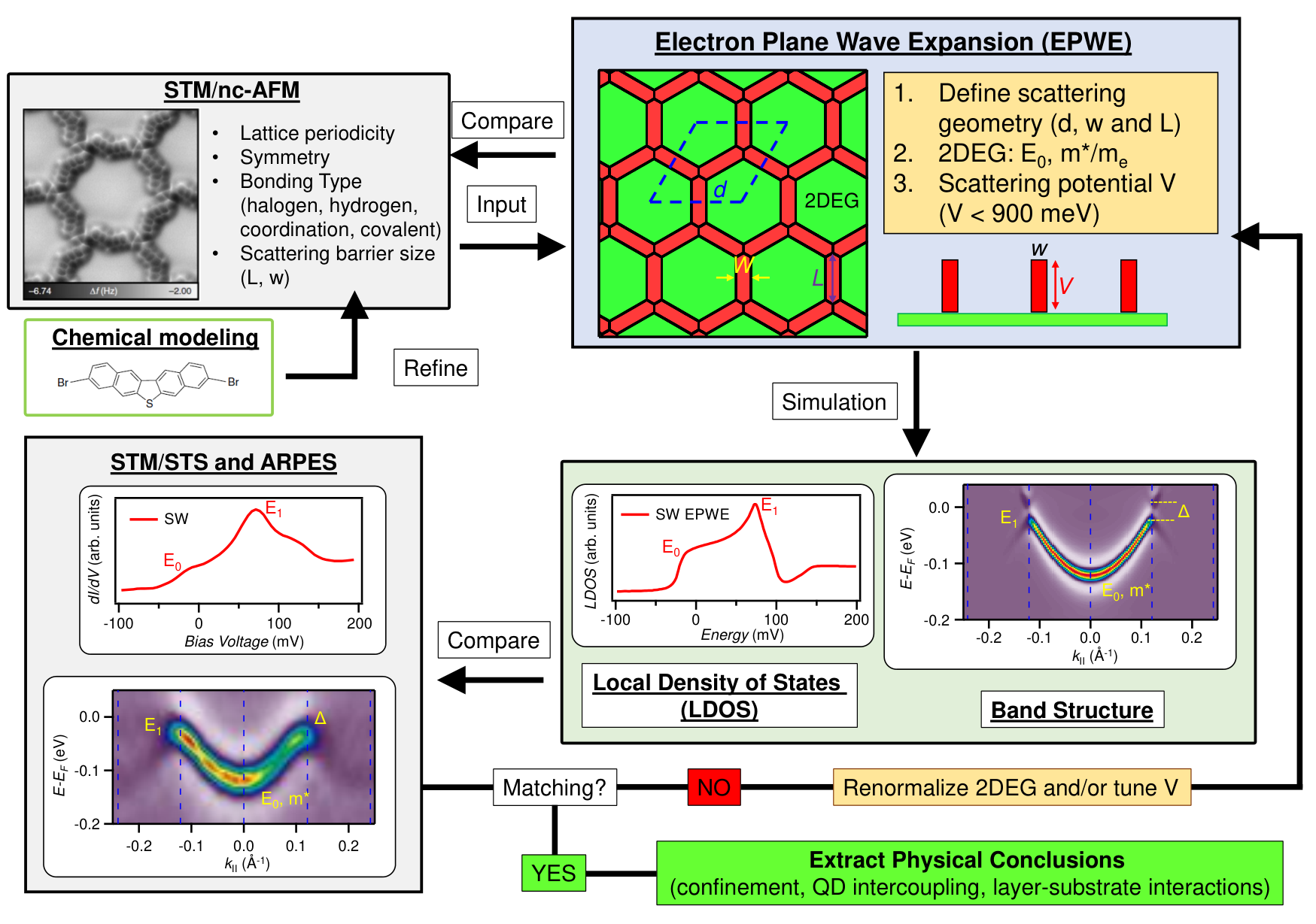
The simulation procedure follows an iterative fitting of different parameters that should systematically lead to a unique physically meaningful solution. Figure 23 displays the recursive process to obtain the scattering potential landscapes based on experimental datasets of electron confining structures:
- 1.
Setting of the scattering geometry. A model of the network (i.e., lattice constant and symmetry), as well as molecular barrier size (L, w) is accurately extracted from STM and nc-AFM images and refined by chemical structures.
- 2.
Definition of the 2DEG. Once the geometry is fixed, parameters from the pristine case are initially used based on their fundamental energy (E0) and effective mass () (see Table 1).
- 3.
Adjusting repulsive scattering barriers. These potential barriers are initially repulsive and limited to meV for carbon-based molecules. Note that this value depends on the molecular backbone size (related to step 1). Whenever metal adatoms are present in the network, a similar potential is assigned, which will likely need reduction in following iterations. Note that will be positive (repulsive), unless bound states are experimentally detected, which has never been the case in porous MOCNs.
- 4.
Simulate the experimental LDOS and band structure. This is the algorithm core: Vary , and the 2DEG renormalization ( and ) to match the fundamental energy () of the QD band, the top of the LDOS peak, the ARPES band () and the gap size between and confined states (). Once the 2DEG has been renormalized to a proper value, and gap size () values depend on and , whereas STS peak-width and ARPES band-width (i.e., -) depend also on . Hence, a refinement of and 2DEG renormalization ( and ) should be carried out iteratively until a satisfactory match with ARPES and STS is found. A more accurate fitting can be obtained whenever higher confined states are introduced by the experiments Piquero-Zulaica et al. 2019c.
- 5.
Extract the parameters once the iteration process does not improve the simulations further. These parameters reflect physically meaningful information on confinement strength, QD intercoupling and energy and mass renormalization effects from the studied network.
Alternatively, it is tempting to envision the inversion of this iterative processes and start by proposing a set of desired electronic features to be realized. In other words, we could consider programming algorithms that would work inversely by yielding experimentally feasible geometries prone to host specific electronic structures. Particularly, theoretical methods have already been proposed that addresses such an ‘inverse approach’ for finding atomic configurations that produce a prescribed electronic structure Franceschetti and Zunger 1999. In this context, descriptors containing the demonstrated electronic scattering and coupling introduced by artificial lattices Gomes et al. 2012; Slot et al. 2017; Kempkes
et al. 2019a; Freeney
et al. 2020a; Kempkes
et al. 2019b; Collins et al. 2017 and/or quantum corrals Li et al. 2020b; Freeney
et al. 2020b could be conceived to develop simplified geometries and engineer nanoarchitectures that target specific electronic effects. Indeed, machine learning procedures are currently at their initial stages and could steer the material research through such data-driven codes that rely on supervised training of the algorithms Ourmazd 2020; Hörmann et al. 2019. Interestingly, such computer coded methods have been recently applied to SPM-based experiments so as to decide upon the data quality and system morphology Alldritt et al. 2020, that are ultimately capable of autonomous operation Krull et al. 2020.
In short, we anticipate that machine learning algorithms could be implemented into the EBEM/EPWE simulations to train and develop new protocols capable of providing the desired band structures from physically meaningful scattering potential landscapes i.e., feasible molecular superlattices. This could be combined with recently developed first-principles/machine-learning algorithms capable of predicting the crystal structure of certain organic molecules on metal surfaces Hörmann et al. 2019. When such geometries are defined, synthetic chemists could fabricate the proposed molecular building blocks and conceive fabrication protocols to be tested experimentally.
VI V. Mutual response of guest species and confined quantum states
We have demonstrated that interfacial 2DEG can be confined and tailored by molecular nanostructures following a proper selection of constituent materials and realization by interfacial synthesis protocols. The energy position of the resonance states and bands, the intercoupling and the final geometry can be defined by the molecular design and the nature of coordination nodes in metallo-supramolecular constructs. However, whenever the confining structure is already set, there is an additional route to tune these electronic states: the deliberate positioning of adsorbed guest species within the confining structures, which can be in the form of organic molecules, single atoms or atom clusters Negulyaev et al. 2008; Cheng et al. 2010; Pivetta et al. 2013; Theobald et al. 2003; Blunt et al. 2010; Teyssandier et al. 2016; Nowakowska et al. 2015.
In the following we describe exemplary cases that reveal how adsorbed species are influenced by the confined LDOS and, in turn, the confined states respond to the presence of adsorbed guest molecules and atoms, similar to single atoms placed in quantum corrals, discussed in the introduction Stepanyuk et al. 2005; Kliewer et al. 2000; Li et al. 2020b; Stilp et al. 2021.
We notably address the interplay regarding organization and electronic response that transition metal atoms, simple molecules or noble gases undergo in the confined 2DEGs of 1D-nanogratings and QD arrays.

VI.1 A. Self-alignment of adspecies in molecular nanogratings
The deposition of 3-metals (Co and Fe) into the 1D-organic nanogratings previously described (cf. Fig. 14) was investigated at low temperatures to follow the electronic structure modifications and the dynamics of the system Schiffrin et al. 2008. Deposition at 8 K of Fe or Co atoms continued by a subtle annealing to 18 K, modifies the randomly distributed guest atom positions, which then self-align as atomic 1D chains at the center of the furrows in the molecular nanogratings [cf. Fig. 24(a)]. Accordingly, this two-stage assembly scenario merges supramolecular organization principles with spontaneous adatom positioning steered by indirect interactions. Interestingly, at sufficiently high local coverage, a preferred distance between individual atoms of 23 Å and 25 Å results for Fe and Co atoms, respectively. This separation reveals a long-range interaction (row-adatom and adatom-adatom) mediated via the QWS, similarly to 2D hexagonal atomic lattices existing on pristine substrates Knorr et al. 2002; Repp et al. 2000; Silly et al. 2004; Negulyaev et al. 2009.
Notably, 0D confinement is found for this system since the guest adatoms act as repulsive scattering barriers to the 1D-confined surface state electrons (the driving force of the atom self-organization). This is evidenced at the LDOS when further tip manipulation procedures are applied to systematically vary the interatomic spacings at the center of a trench, which allows for the fabrication of the tiniest quantum dots [Fig. 24(b)] Pennec et al. 2007. The STS lineshapes in Fig. 24(c) display the familiar QD signatures of Fig. 15(e) instead of the QWS of Figs. 11 and 14. Minima in the interaction energy between the atoms and the resonator boundaries are theoretically expected and observed for both metals when located at the center of the 1D-trenches Schiffrin et al. 2008; Han and Weiss 2012. In essence, employing self-aligning atomic strings, we can modify the dimensionality and onsets of the confined states. This methodology can be generally employed for nanoscale control of matter and for the positioning of single atomic or molecular species in surface-supported supramolecular architectures. In this regard, the positioning and mobility of tetracene molecules in such methionine nanogratings has been studied Urgel et al. 2016a. In addition, it was demonstrated that the spin polarization of surface electrons caused by magnetic adatoms can be projected to a remote location by quantum states of corrals Stepanyuk et al. 2005. In particular, the exchange interaction between magnetic atoms is operative at appreciable distances and a similar behavior is expected for magnetic atoms organized in such 1D nanogratings or QD arrays Pennec et al. 2007; Pivetta et al. 2013 [see Fig. 24(a) and Fig. 25(c)].

VI.2 B. Guided adsorption of adatoms and simple molecules in QD arrays
The presence of a 2DEG can strongly influence the self-assembly processes of the adsorbed species Wang et al. 2009. This is also the case whenever the surface state is confined. As a first example we show the adsorption of CO molecules at the pores of the chiral anthraquinone (AQ) network grown on Cu(111) Cheng et al. 2010 [see Fig. 25(a), (b)]. This AQ network presents one of the largest regular pore areas since the self-assembly is mediated by C-H-O interactions that involve 18 molecules Pawin et al. 2006; Cheng et al. 2010; Wyrick et al. 2011.
At 40 K, the diffusion of the CO molecules is restricted to a single pore and dynamic processes confirm their repulsive character Cheng et al. 2010. Indeed, a hierarchy of preferred adsorption sites prevails, depending on the number of CO molecules captured within a pore. For a single CO molecule, the center of the network cavity is favored and maintained whenever a second CO molecule is added, which then sits on a midway site between the pore center and edge. Higher number of captured COs will preferentially occupy any available halfway adsorption site. Simulations on this system conclude that the first and second confined states (in this order) drive the CO adsorption positions Cheng et al. 2010, so CO molecules seize adsorption sites with high LDOS. Therefore, the diffusion is not limited just by the physical barriers (molecules), but also by the modified LDOS generated by the QD array Einstein et al. 2018.
Similarly, the arrangement of Fe atoms follows a related scheme when filling the pores of dicyano-poly(p-phenylene) based MOCNs Pivetta et al. 2013. Particularly, the adsorption of Fe atoms onto a Ph5+Cu MOCN assembled on Cu(111) preferentially follows electron-mediated interactions between the adatoms, which are reinforced by the cavity confined surface electrons [Fig. 25(c)]. Thus, a certain control over the guest species assemblies is exerted by proper selection of the network used as confining template. Similar to the atomic chains in supramolecular nanogrids described above, this process requires thermal activation, and upon overcoming the formation energy barrier discrete Fe clusters in the pores are obtained.
The last example considered studies the adsorption of Xe noble gas atoms into the well characterized DPDI+Cu network Nowakowska et al. 2015; Nowakowska et al. 2016; Ahsan et al. 2018; Ahsan et al. 2019. The atom-by-atom condensation leads to a maximum occupation of 12 Xe guests that do not follow a single set of hierarchic filling rule, but adapt their structures with their neighbors Nowakowska et al. 2015; Nowakowska et al. 2016 [see Fig. 25(d)]. This pore saturation exhibits tetramer grouping with Xe atoms adsorbed at on-top sites of the Cu(111) atomic lattice, resulting in a ()R30∘ overlayer structure that coincides with the direct adsorption of Xe on pristine Cu(111) Seyller et al. 1998. This tetramer grouping matches the three-fold symmetry of the DPDI network with respect to the substrate Piquero-Zulaica
et al. 2019c. In other words, the confined state –closest to the Fermi energy– appears to guide the Xe condensation. Alternatively, these Xe atoms could be just marking the three equivalent metal coordination sites that exhibit the lowest surface potential of the network Dil et al. 2008; Piquero-Zulaica
et al. 2019c.

In this context, it is also interesting to note that any mobility of hosted species entails a temporally fluctuating confinement geometry. Thus monomers or trimeric units caged in nanoporous honeycomb MOCNs are expected to present dynamic confinement patterns, which can vary rapidly and account for rather complex electronic configurations Kühne et al. 2010; Palma et al. 2014; Palma et al. 2015.
VI.3 C. Configuring QD states by manipulation of guest adsorbates
The Xe occupation and its effect on the QD electronic properties was investigated with respect to its adjacent neighbors on the DPDI+Cu network Nowakowska et al. 2016. This system was chosen because Xe is physisorbed within these pores and can be atomically manipulated using a STM tip. In this way, artificial intermediate situations can be created between empty and saturated pores, simulating an electronic breadboard [cf. Figure 26(a)-(d)]. The empty pore case has been electronically addressed in Figs. 18 and 19 and exhibits a broad confined peak with maximum around V that relates to the first QD array band [cf. Fig. 26(a)]. Upon Xe saturation, this confined state peak shifts by mV towards the Fermi level. This upshift effect is attributed to Pauli repulsion between the rare gases and the confined states Park et al. 2000; Hövel et al. 2001; Forster et al. 2004. Note that the broad peak width remains since the Xe physisorption at the pores does not practically modify the interpore coupling, as evidenced in ARPES measurements Nowakowska et al. 2016.
Intermediate cases, achieved through atomic manipulation, yield a single filled pore within an empty network [Fig. 26(c)] and an empty pore embedded in a Xe saturated network [Fig. 26(d)]. Different occupation dependent electronic states (QD states) are observed that display shifted energy maxima. In practice, the isolated filled pore shows a delta-like (non-coupled) confined state peaking close to the Xe filled network energy [Fig. 26(b)], whereas the empty one displays a broad peak close to the fundamental energy of the DPDI+Cu network [Fig. 26(a)]. Note that the neighboring pores appear electronically unaffected by these local cases, so for the overall system they can be considered as isolated defects.
EPWE was used to simulate the Xe-induced effect in these four cases and gain insight into confinement strength and QD coupling. The simulated LDOS depicted in the bottom row of Figure 26 uses scattering potentials of meV (from Table 2) and meV at the occupied pores to account for the Pauli repulsion effect induced by the Xe adatoms. Not only the energy shifts, but also the confined state peakwidths and shapes are accurately matched. From these simulations we conclude that the presence of Xe at the pores generates an energy upshift of the confined states that maintain extended Bloch waves because the interpore coupling is not affected. The fact that the peak energies are markedly different between Xe filled and empty pores indicates that this system can be used as an electronic breadboard to store information with a bit areal density of bits/cm2, by far exceeding current hard disk storage densities.
VII VI. Conclusions and outlook
Throughout this review we have shown the wide range of possibilities that molecular nanoarchitectures provide for confining and engineering surface 2D electron gases. The chemical versatility provides a multitude of opportunities to generate molecular assemblies featuring the desired scattering potential barriers that control surface electrons and shape the interfacial electronic landscape. Ultimately, these quantum properties depend on the physicochemical nature of the selected building units. Although we have focused on the fcc(111) surfaces of copper, silver and gold, the elaborated principles are extensible to many other system exhibiting quasi-free electrons on their surface, such as 3D topological insulators, surface alloys, 2D materials or thin film superconductors. To date, similar molecular structures onto such surfaces reemain practically unexplored.
The desired structures can be obtained by tip manipulation, by molecular self-assembly protocols, or a combination of both. Such building methods have substantially expanded the available toolbox initially limited to atom corrals and vicinal surfaces. We have shown that the molecular structures are extremely versatile, whereby all the confining parameters and the QD intercoupling degree among repeating units can be addressed. This bears the prospect of efficient fabrication of confining structures at the technological level and miniaturization for device integration.
The experimental and theoretical cases we reviewed reveal the deep insight into the scattering potential configurations that molecular nanoarchitectures and networks represent for surface electrons. While molecules typically exhibit strong repulsive potential barriers for the 2DEG electrons, adatoms are less predictable, and are generally weaker in their scattering strength. Nonetheless, they present the remarkable property of renormalizing significantly the pristine surface state onset and as coordination nodes can open channels to enhance the QD intercoupling. In essence, molecule-based networks with pores modulate the 2DEG through the potential barriers they produce and can generate distinct band structures that can be easily engineered through self-assembly protocols.
We also showed that the positioning of guest species at nanogrids or network pores provides an extra route to alter the confined electronic states. Systems with significant energy differences between occupied and empty states could be also used as breadboards to engineer artificial lattices. These electronic breadboards are envisioned as operating COFs or nanoporous graphenes (NPGs) as they are stable and manipulable at room temperature.
The semiempirical methods used to model these networks have significantly improved over the years and can convincingly reconstruct the scattering potential landscape responsible for the 2DEG confinement. Nowadays we can envision the use of machine learning to propose molecular geometries that induce the electronic properties we ultimately desire. Such machine learning processes could be based on the inverse EPWE methodology discussed. This procedure could guide the design of novel artificial molecular lattices beyond the ones already explored.

The survey of the many examples reveals that a rationale is about to be established in this field, which is reaching its maturity. It provides nowadays the ability, ingredients and methodology to generate well-defined molecular (and atomic) nanoarchitectures that can open up many future opportunities for interfacial electronic structure and functionality design.
A vast playground is at hand to transfer, for example, optical effects into low-dimensional quantum systems given our ability to directly image the QPI patterns generated by these nanostructures, with the benefit of a 1000-fold reduction in wavelength and structural parameters García de Abajo
et al. 2010. For instance, exotic refraction anomalies leading to few nanometer electron focusing (collimation) or negative refraction and beam splitting has been predicted for triangular superlattices [see Figure 27(a,b)] García de Abajo
et al. 2010; Abd El-Fattah et al. 2017. Optical-like effects, such as lateral electron refraction have already been observed in simpler 2D systems, allowing the validation of Snell’s law for electronic waves Repp et al. 2004 [see Figure 27(c)]. Likewise, diffraction and interference patterns analogous to photons in coupled waveguides (Talbot effect) have been predicted in NPGs due to the presence of Dirac cones in the band structure Moreno et al. 2018; Calogero et al. 2019 [Figure 27(d)]. The existence of these topological signatures in artificial lattices and networks should promote similar optical-like properties in selected 2DEG scattering nanostructures. A relevant prospect is the replication of the quantum holography concept by means of artificial lattices that overcame the single-atom limit for information storage density Moon et al. 2009. Indeed, the introduction of magnetism into the system could double the information density as compared to the volumetric quantum holographic encoding, which could be experimentally accessible using a spin-polarized STM Brovko and Stepanyuk 2012.

Novel quantum properties are also envisioned by further engineering these 2DEGs. In particular, electronic scattering and confinement effects should be transferable to image potential states, that are accessible via STS or 2PPE techniques Niesner and Fauster 2014; Echenique et al. 2004; Schouteden and Van Haesendonck 2012. Likewise, these network modified 2DEGs have been recently proposed to play a key role in the stabilization and significant energy downshifting of super-atom molecular orbital (SAMO) states Kawai et al. 2021. These states of molecular origin feature a very localized and high DOS at small pores ( nm wide) that could be envisioned for further applications Zhang et al. 2016b; Hieulle et al. 2018; Moreno et al. 2018; Kawai et al. 2021.
From a fundamental perspective, further action is required beyond the 2DEG scattering and confinement properties in these molecule-based networks. For example, validation of predicted MOCNs as organic topological insulators, superconductors, quantum spin liquid systems or ferromagnets still awaits Zhang et al. 2016a; Kumar et al. 2018; Zhang et al. 2020b; Gao et al. 2019; Sun et al. 2018; Dong et al. 2016b; Wang et al. 2013a; Gao et al. 2020; Zhang et al. 2017; Hernández-López
et al. 2021 [Fig. 28(a)]. Likewise, the synthesis of atomically perfect, periodic and extended nanoporous 2D-COFs is still experimentally pending Bieri et al. 2009; Galeotti et al. 2020. Formation of such topological array should likely originate from a particular, pre-arranged, well-defined and extended nanoporous network. The expected technological relevance of such covalent networks is huge since they could be used as 2D stamps, so that these structures could be transferred to other relevant supports. Also, as illustrated in Fig. 28(b), the pores could introduce anisotropy into the electronic transport (as for NPG structures) or provide functionality in the form of gas selectivity or catalysing activity in industrially relevant processes Moreno et al. 2018; Jacobse et al. 2020.
From a practical point of view these emerging quantum states of matter should be made extensible to non-metal substrates such as 2D layered materials, topological insulators, semiconductors, superconducting substrates or hybrid structures, which are considered to be the base for future device architectures Gobbi et al. 2018 [Fig. 28(c)]. Steps to make this a reality are currently underway, since, for example, molecular networks have been used to alter the graphene properties by inducing an extended and atomically precise covalent coupling between layers Yu et al. 2020. All in all, (metal-)organic nanoporous networks as the ones here described bear the prospect of being excellent technological candidates for the quantum era ahead of us.
VIII Acknowledgements
IPZ, JLC and EO acknowledge the financial support from the Spanish Ministry of Economy, Industry and Competitiveness (MINECO, Grant No. PID2019-107338RB-C6-3 and PID2019-107338RB-C6-4) from the regional Government of Aragon (Grant No. E12-20R) and the Basque Government (IT-1255-19) and from the European Regional Development Fund (ERDF) under the program Interreg V-A España-Francia-Andorra (Contract No. EFA 194/16 TNSI).
WA acknowledges funding from the German Research Foundation (DFG, Heisenberg professorship) and the ERC Consolidator Grant NanoSurfs, and JVB support via DFG (BA 3395/2-1), ERC (Advanced Grant MolArt), as well as the DFG Excellence Cluster Munich Center of Quantum Science and Technology (MCQST).
We are grateful to all graduate students, cooperation partners and colleagues coauthoring original work.
References
- Klitzing et al. (1980) K. v. Klitzing, G. Dorda, and M. Pepper, Phys Rev Lett 45, 494 (1980).
- Shechtman et al. (1984) D. Shechtman, I. Blech, D. Gratias, and J. W. Cahn, Phys Rev Lett 53, 1951 (1984).
- Amano et al. (1986) H. Amano, N. Sawaki, I. Akasaki, and Y. Toyoda, Appl Phys Lett 48, 353 (1986).
- Heeger et al. (1988) A. J. Heeger, S. Kivelson, J. R. Schrieffer, and W. P. Su, Rev Mod Phys 60, 781 (1988).
- Binasch et al. (1989) G. Binasch, P. Grünberg, F. Saurenbach, and W. Zinn, Phys Rev B 39, 4828 (1989).
- Davis et al. (1995) K. B. Davis, M. O. Mewes, M. R. Andrews, N. J. van Druten, D. S. Durfee, D. M. Kurn, and W. Ketterle, Phys Rev Lett 75, 3969 (1995).
- Kane and Mele (2005) C. L. Kane and E. J. Mele, Phys Rev Lett 95, 146802 (2005).
- Bloch et al. (2008) I. Bloch, J. Dalibard, and W. Zwerger, Rev Mod Phys 80, 885 (2008).
- Mühlbauer et al. (2009) S. Mühlbauer, B. Binz, F. Jonietz, C. Pfleiderer, A. Rosch, A. Neubauer, R. Georgii, and P. Böni, Science 323, 915 (2009).
- Müller (1965) E. W. Müller, Science 149, 591 (1965).
- Binnig and Rohrer (1987) G. Binnig and H. Rohrer, Rev Mod Phys 59, 615 (1987).
- Stroscio and Eigler (1991) J. A. Stroscio and D. M. Eigler, Science 254, 1319 (1991).
- Damascelli et al. (2003) A. Damascelli, Z. Hussain, and Z.-X. Shen, Rev Mod Phys 75, 473 (2003).
- Lobo-Checa et al. (2009) J. Lobo-Checa, M. Matena, K. Müller, J. H. Dil, F. Meier, L. H. Gade, T. A. Jung, and M. Stöhr, Science 325, 300 (2009).
- Gambardella et al. (2003) P. Gambardella, S. Rusponi, M. Veronese, S. S. Dhesi, C. Grazioli, A. Dallmeyer, I. Cabria, R. Zeller, P. H. Dederichs, K. Kern, et al., Science 300, 1130 (2003).
- Klappenberger (2014) F. Klappenberger, Prog Surf Sci 89, 1 (2014).
- Galeotti et al. (2020) G. Galeotti, F. De Marchi, E. Hamzehpoor, O. MacLean, M. Rajeswara Rao, Y. Chen, L. V. Besteiro, D. Dettmann, L. Ferrari, F. Frezza, et al., Nat Mater 19, 874 (2020).
- Yin et al. (2021) J.-X. Yin, S. H. Pan, and M. Zahid Hasan, Nature Reviews Physics 3, 249 (2021).
- Barth et al. (2000) J. V. Barth, J. Weckesser, C. Cai, P. Günter, L. Bürgi, O. Jeandupeux, and K. Kern, Angew Chem Int Ed 39, 1230 (2000).
- Theobald et al. (2003) J. A. Theobald, N. S. Oxtoby, M. A. Phillips, N. R. Champness, and P. H. Beton, Nature 424, 1029 (2003).
- Yokoyama et al. (2001) T. Yokoyama, S. Yokoyama, T. Kamikado, Y. Okuno, and S. Mashiko, Nature 413, 619 (2001).
- Stepanow et al. (2004) S. Stepanow, M. Lingenfelder, A. Dmitriev, H. Spillmann, E. Delvigne, N. Lin, X. Deng, C. Cai, J. V. Barth, and K. Kern, Nat Mater 3, 229 (2004).
- Barth et al. (2005) J. V. Barth, G. Costantini, and K. Kern, Nature 437, 671 (2005).
- Kühnle (2009) A. Kühnle, Current Opinion in Colloid & Interface Science 14, 157 (2009).
- Kudernac et al. (2009) T. Kudernac, S. Lei, J. A. A. W. Elemans, and S. De Feyter, Chem Soc Rev 38, 402 (2009).
- Dong et al. (2016a) L. Dong, Z. Gao, and N. Lin, Prog Surf Sci 91, 101 (2016a).
- Goronzy et al. (2018) D. P. Goronzy, M. Ebrahimi, F. Rosei, Arramel, Y. Fang, S. De Feyter, S. L. Tait, C. Wang, P. H. Beton, A. T. S. Wee, et al., ACS Nano 12, 7445 (2018).
- Xing et al. (2019) L. Xing, Z. Peng, W. Li, and K. Wu, Acc Chem Res 52, 1048 (2019).
- Stöhr et al. (2007) M. Stöhr, M. Wahl, H. Spillmann, L. Gade, and T. Jung, Small 3, 1336 (2007).
- Kühne et al. (2010) D. Kühne, F. Klappenberger, W. Krenner, S. Klyatskaya, M. Ruben, and J. V. Barth, Proceedings of the National Academy of Sciences 107, 21332 (2010).
- Pivetta et al. (2013) M. Pivetta, G. E. Pacchioni, U. Schlickum, J. V. Barth, and H. Brune, Phys Rev Lett 110, 086102 (2013).
- Nowakowska et al. (2016) S. Nowakowska, A. Wäckerlin, I. Piquero-Zulaica, J. Nowakowski, S. Kawai, C. Wäckerlin, M. Matena, T. Nijs, S. Fatayer, O. Popova, et al., Small 12, 3759 (2016).
- Zhang et al. (2015) R. Zhang, G. Lyu, C. Chen, T. Lin, J. Liu, P. N. Liu, and N. Lin, ACS Nano 9, 8547 (2015).
- Nowakowska et al. (2015) S. Nowakowska, A. Wäckerlin, S. Kawai, T. Ivas, J. Nowakowski, S. Fatayer, C. Wäckerlin, T. Nijs, E. Meyer, J. Björk, et al., Nat Commun 6, 6071 (2015).
- Teyssandier et al. (2016) J. Teyssandier, S. D. Feyter, and K. S. Mali, Chem Commun 52, 11465 (2016).
- Kocić et al. (2019) N. Kocić, D. Blank, P. Abufager, N. Lorente, S. Decurtins, S.-X. Liu, and J. Repp, Nano Lett 19, 2750 (2019).
- Gutzler et al. (2015) R. Gutzler, S. Stepanow, D. Grumelli, M. Lingenfelder, and K. Kern, Acc Chem Res 48, 2132 (2015).
- echal et al. (2016) J. echal, C. S. Kley, R. Pétuya, F. Schramm, M. Ruben, S. Stepanow, A. Arnau, and K. Kern, The Journal of Physical Chemistry C 120, 18622 (2016).
- Écija et al. (2018) D. Écija, J. I. Urgel, A. P. Seitsonen, W. Auwärter, and J. V. Barth, Acc Chem Res 51, 365 (2018).
- Umbach et al. (2012) T. R. Umbach, M. Bernien, C. F. Hermanns, A. Krüger, V. Sessi, I. Fernandez-Torrente, P. Stoll, J. I. Pascual, K. J. Franke, and W. Kuch, Phys Rev Lett 109, 267207 (2012).
- Abdurakhmanova et al. (2013) N. Abdurakhmanova, T.-C. Tseng, A. Langner, C. S. Kley, V. Sessi, S. Stepanow, and K. Kern, Phys Rev Lett 110, 027202 (2013).
- Gao et al. (2020) Z. Gao, Y. Gao, M. Hua, J. Liu, L. Huang, and N. Lin, The Journal of Physical Chemistry C 124, 27017 (2020).
- Hötger et al. (2019) D. Hötger, M. Etzkorn, C. Morchutt, B. Wurster, J. Dreiser, S. Stepanow, D. Grumelli, R. Gutzler, and K. Kern, Phys Chem Chem Phys 21, 2587 (2019).
- Li et al. (2012) Y. Li, J. Xiao, T. E. Shubina, M. Chen, Z. Shi, M. Schmid, H.-P. Steinrück, J. M. Gottfried, and N. Lin, J Am Chem Soc 134, 6401 (2012).
- Urgel et al. (2016a) J. I. Urgel, D. Écija, G. Lyu, R. Zhang, C.-A. Palma, W. Auwärter, N. Lin, and J. V. Barth, Nat Chem 8, 657 (2016a).
- Zhang et al. (2018) Y.-Q. Zhang, M. Paszkiewicz, P. Du, L. Zhang, T. Lin, Z. Chen, S. Klyatskaya, M. Ruben, A. P. Seitsonen, J. V. Barth, et al., Nat Chem 10, 296 (2018).
- Yan et al. (2017) L. Yan, G. Kuang, Q. Zhang, X. Shang, P. N. Liu, and N. Lin, Faraday Discuss 204, 111 (2017).
- Zhang et al. (2016a) L. Z. Zhang, Z. F. Wang, B. Huang, B. Cui, Z. Wang, S. X. Du, H.-J. Gao, and F. Liu, Nano Lett 16, 2072 (2016a).
- Kumar et al. (2018) A. Kumar, K. Banerjee, A. S. Foster, and P. Liljeroth, Nano Lett 18, 5596 (2018).
- Gao et al. (2019) Z. Gao, C.-H. Hsu, J. Liu, F.-C. Chuang, R. Zhang, B. Xia, H. Xu, L. Huang, Q. Jin, P. N. Liu, et al., Nanoscale 11, 878 (2019).
- Sun et al. (2018) H. Sun, S. Tan, M. Feng, J. Zhao, and H. Petek, The Journal of Physical Chemistry C 122, 18659 (2018).
- Dong et al. (2016b) L. Dong, Y. Kim, D. Er, A. M. Rappe, and V. B. Shenoy, Phys Rev Lett 116, 096601 (2016b).
- Wang et al. (2013a) Z. F. Wang, Z. Liu, and F. Liu, Nat Commun 4, 1471 (2013a).
- Hernández-López et al. (2021) L. Hernández-López, I. Piquero-Zulaica, C. A. Downing, M. Piantek, J. Fujii, D. Serrate, J. E. Ortega, F. Bartolomé, and J. Lobo-Checa, Nanoscale 13, 5216 (2021).
- Jiang et al. (2021) W. Jiang, X. Ni, and F. Liu, Acc Chem Res 54, 416 (2021).
- Gomes et al. (2012) K. K. Gomes, W. Mar, W. Ko, F. Guinea, and H. C. Manoharan, Nature 483, 306 (2012).
- Slot et al. (2017) M. R. Slot, T. S. Gardenier, P. H. Jacobse, G. C. P. van Miert, S. N. Kempkes, S. J. M. Zevenhuizen, C. M. Smith, D. Vanmaekelbergh, and I. Swart, Nat Phys 13, 672 (2017).
- Kempkes et al. (2019a) S. N. Kempkes, M. R. Slot, J. J. van den Broeke, P. Capiod, W. A. Benalcazar, D. Vanmaekelbergh, D. Bercioux, I. Swart, and C. Morais Smith, Nat Mater 18, 1292 (2019a).
- Freeney et al. (2020a) S. E. Freeney, J. J. van den Broeke, A. J. J. Harsveld van der Veen, I. Swart, and C. Morais Smith, Phys Rev Lett 124, 236404 (2020a).
- Kempkes et al. (2019b) S. N. Kempkes, M. R. Slot, S. E. Freeney, S. J. M. Zevenhuizen, D. Vanmaekelbergh, I. Swart, and C. M. Smith, Nat Phys 15, 127 (2019b).
- Collins et al. (2017) L. C. Collins, T. G. Witte, R. Silverman, D. B. Green, and K. K. Gomes, Nat Commun 8, 15961 (2017).
- Cao et al. (2018a) Y. Cao, V. Fatemi, S. Fang, K. Watanabe, T. Taniguchi, E. Kaxiras, and P. Jarillo-Herrero, Nature 556, 43 (2018a).
- Cao et al. (2018b) Y. Cao, V. Fatemi, A. Demir, S. Fang, S. L. Tomarken, J. Y. Luo, J. D. Sanchez-Yamagishi, K. Watanabe, T. Taniguchi, E. Kaxiras, et al., Nature 556, 80 (2018b).
- Ketterle (2002) W. Ketterle, Rev Mod Phys 74, 1131 (2002).
- Zapf et al. (2014) V. Zapf, M. Jaime, and C. D. Batista, Rev Mod Phys 86, 563 (2014).
- Park and Louie (2009a) C.-H. Park and S. G. Louie, Nano Lett 9, 1793 (2009a).
- Polini et al. (2013) M. Polini, F. Guinea, M. Lewenstein, H. C. Manoharan, and V. Pellegrini, Nat Nanotechnol 8, 625 (2013).
- Leykam et al. (2018) D. Leykam, A. Andreanov, and S. Flach, Advances in Physics: X 3, 1473052 (2018).
- Greiner et al. (2002) M. Greiner, O. Mandel, T. Esslinger, T. W. Hänsch, and I. Bloch, Nature 415, 39 (2002).
- Duke (2003) C. B. Duke, Proceedings of the National Academy of Sciences 100, 3858 (2003).
- Gross et al. (2004) L. Gross, F. Moresco, L. Savio, A. Gourdon, C. Joachim, and K.-H. Rieder, Phys Rev Lett 93, 056103 (2004).
- Pennec et al. (2007) Y. Pennec, W. Auwärter, A. Schiffrin, A. Weber-Bargioni, A. Riemann, and J. V. Barth, Nat Nanotechnol 2, 99 (2007).
- Klappenberger et al. (2009) F. Klappenberger, D. Kühne, W. Krenner, I. Silanes, A. Arnau, F. J. García de Abajo, S. Klyatskaya, M. Ruben, and J. V. Barth, Nano Lett 9, 3509 (2009).
- Cheng et al. (2010) Z. Cheng, J. Wyrick, M. Luo, D. Sun, D. Kim, Y. Zhu, W. Lu, K. Kim, T. L. Einstein, and L. Bartels, Phys Rev Lett 105, 066104 (2010).
- Wang et al. (2013b) S. Wang, W. Wang, L. Z. Tan, X. G. Li, Z. Shi, G. Kuang, P. N. Liu, S. G. Louie, and N. Lin, Phys Rev B: Condens Matter Mater Phys 88, 245430 (2013b).
- Müller et al. (2016) K. Müller, M. Enache, and M. Stöhr, J Phys : Condens Matter 28, 153003 (2016).
- Martín-Jiménez et al. (2019) A. Martín-Jiménez, J. M. Gallego, R. Miranda, and R. Otero, Phys Rev Lett 122, 176801 (2019).
- Ashcroft and Mermin (1976) N. W. Ashcroft and N. D. Mermin, Solid state physics (Holt, Rinehart and Winston, New York, 1976).
- Brennan (1999) K. F. Brennan, The Physics of Semiconductors: With Applications to Optoelectronic Devices (Cambridge University Press, 1999), 1st ed.
- Yoffe (2001) A. D. Yoffe, Adv Phys 50, 1 (2001).
- Zwanenburg et al. (2013) F. A. Zwanenburg, A. S. Dzurak, A. Morello, M. Y. Simmons, L. C. L. Hollenberg, G. Klimeck, S. Rogge, S. N. Coppersmith, and M. A. Eriksson, Rev Mod Phys 85, 961 (2013).
- van Wees et al. (1988) B. J. van Wees, H. van Houten, C. W. J. Beenakker, J. G. Williamson, L. P. Kouwenhoven, D. van der Marel, and C. T. Foxon, Phys Rev Lett 60, 848 (1988).
- Kanisawa et al. (2001) K. Kanisawa, M. J. Butcher, H. Yamaguchi, and Y. Hirayama, Phys Rev Lett 86, 3384 (2001).
- Sato and Ando (2017) M. Sato and Y. Ando, Rep Prog Phys 80, 076501 (2017).
- Nayak et al. (2008) C. Nayak, S. H. Simon, A. Stern, M. Freedman, and S. Das Sarma, Rev Mod Phys 80, 1083 (2008).
- Choi et al. (2019) D.-J. Choi, N. Lorente, J. Wiebe, K. von Bergmann, A. F. Otte, and A. J. Heinrich, Rev Mod Phys 91, 041001 (2019).
- Harrison (2005) P. Harrison, Quantum Wells, Wires and Dots: Theoretical and Computational Physics of Semiconductor Nanostructures (John Wiley & Sons, Ltd, Chichester, UK, 2005).
- van der Wiel et al. (2002) W. G. van der Wiel, S. De Franceschi, J. M. Elzerman, T. Fujisawa, S. Tarucha, and L. P. Kouwenhoven, Rev Mod Phys 75, 1 (2002).
- Hanson et al. (2007) R. Hanson, L. P. Kouwenhoven, J. R. Petta, S. Tarucha, and L. M. K. Vandersypen, Rev Mod Phys 79, 1217 (2007).
- Pekola et al. (2013) J. P. Pekola, O.-P. Saira, V. F. Maisi, A. Kemppinen, M. Möttönen, Y. A. Pashkin, and D. V. Averin, Rev Mod Phys 85, 1421 (2013).
- Wharam et al. (1988) D. A. Wharam, T. J. Thornton, R. Newbury, M. Pepper, H. Ahmed, J. E. F. Frost, D. G. Hasko, D. C. Peacock, D. A. Ritchie, and G. A. C. Jones, J Phys C: Solid State Phys 21, L209 (1988).
- Ohnishi et al. (1998) H. Ohnishi, Y. Kondo, and K. Takayanagi, Nature 395, 780 (1998).
- Tarucha et al. (1996) S. Tarucha, D. G. Austing, T. Honda, R. J. van der Hage, and L. P. Kouwenhoven, Phys Rev Lett 77, 3613 (1996).
- Kagan and Murray (2015) C. R. Kagan and C. B. Murray, Nat Nanotechnol 10, 1013 (2015).
- Kagan et al. (2016) C. R. Kagan, E. Lifshitz, E. H. Sargent, and D. V. Talapin, Science 353, aac5523 (2016).
- Broome et al. (2018) M. A. Broome, S. K. Gorman, M. G. House, S. J. Hile, J. G. Keizer, D. Keith, C. D. Hill, T. F. Watson, W. J. Baker, L. C. L. Hollenberg, et al., Nat Commun 9, 980 (2018).
- Leon et al. (2020) R. C. C. Leon, C. H. Yang, J. C. C. Hwang, J. C. Lemyre, T. Tanttu, W. Huang, K. W. Chan, K. Y. Tan, F. E. Hudson, K. M. Itoh, et al., Nat Commun 11, 797 (2020).
- Walkup et al. (2020) D. Walkup, F. Ghahari, C. Gutiérrez, K. Watanabe, T. Taniguchi, N. B. Zhitenev, and J. A. Stroscio, Phys Rev B: Condens Matter Mater Phys 101, 035428 (2020).
- Tokura et al. (2017) Y. Tokura, M. Kawasaki, and N. Nagaosa, Nat Phys 13, 1056 (2017).
- Keimer and Moore (2017) B. Keimer and J. E. Moore, Nat Phys 13, 1045 (2017).
- Huang et al. (2017) B. Huang, G. Clark, E. Navarro-Moratalla, D. R. Klein, R. Cheng, K. L. Seyler, D. Zhong, E. Schmidgall, M. A. McGuire, D. H. Cobden, et al., Nature 546, 270 (2017).
- Gong et al. (2017) C. Gong, L. Li, Z. Li, H. Ji, A. Stern, Y. Xia, T. Cao, W. Bao, C. Wang, Y. Wang, et al., Nature 546, 265 (2017).
- Andrei and MacDonald (2020) E. Y. Andrei and A. H. MacDonald, Nat Mater 19, 1265 (2020).
- Kezilebieke et al. (2020) S. Kezilebieke, M. N. Huda, V. Vaňo, M. Aapro, S. C. Ganguli, O. J. Silveira, S. Głodzik, A. S. Foster, T. Ojanen, and P. Liljeroth, Nature 588, 424 (2020).
- Li et al. (2021) H. Li, S. Li, M. H. Naik, J. Xie, X. Li, J. Wang, E. Regan, D. Wang, W. Zhao, S. Zhao, et al., Nat Mater (2021).
- Reinert et al. (2001) F. Reinert, G. Nicolay, S. Schmidt, D. Ehm, and S. Hüfner, Phys Rev B: Condens Matter Mater Phys 63, 115415 (2001).
- Shockley (1939) W. Shockley, Phys Rev 56, 317 (1939).
- Kevan and Gaylord (1987) S. D. Kevan and R. H. Gaylord, Phys Rev B 36, 5809 (1987).
- Paniago et al. (1995a) R. Paniago, R. Matzdorf, G. Meister, and A. Goldmann, Surf Sci 331-333, 1233 (1995a).
- Reinert and Hüfner (2005) F. Reinert and S. Hüfner, New J Phys 7, 97 (2005).
- Malterre et al. (2007) D. Malterre, B. Kierren, Y. Fagot-Revurat, S. Pons, A. Tejeda, C. Didiot, H. Cercellier, and A. Bendounan, New J Phys 9, 391 (2007).
- Oka et al. (2014) H. Oka, O. O. Brovko, M. Corbetta, V. S. Stepanyuk, D. Sander, and J. Kirschner, Rev Mod Phys 86, 1127 (2014).
- Tamai et al. (2013) A. Tamai, W. Meevasana, P. D. C. King, C. W. Nicholson, A. de la Torre, E. Rozbicki, and F. Baumberger, Phys Rev B: Condens Matter Mater Phys 87, 075113 (2013).
- Paniago et al. (1995b) R. Paniago, R. Matzdorf, G. Meister, and A. Goldmann, Surf Sci 336, 113 (1995b).
- LaShell et al. (1996) S. LaShell, B. A. McDougall, and E. Jensen, Phys Rev Lett 77, 3419 (1996).
- Yan et al. (2015) B. Yan, B. Stadtmüller, N. Haag, S. Jakobs, J. Seidel, D. Jungkenn, S. Mathias, M. Cinchetti, M. Aeschlimann, and C. Felser, Nat Commun 6, 10167 (2015).
- Tersoff and Hamann (1985) J. Tersoff and D. R. Hamann, Phys Rev B 31, 805 (1985).
- Crommie et al. (1993a) M. F. Crommie, C. P. Lutz, and D. M. Eigler, Nature 363, 524 (1993a).
- Crommie et al. (1993b) M. F. Crommie, C. P. Lutz, and D. M. Eigler, Science 262, 218 (1993b).
- Bertel and Memmel (1996) E. Bertel and N. Memmel, Applied Physics A Materials Science and Processing 63, 523 (1996).
- Kulawik et al. (2005) M. Kulawik, H.-P. Rust, M. Heyde, N. Nilius, B. A. Mantooth, P. S. Weiss, and H.-J. Freund, Surf Sci 590, L253 (2005).
- Hasegawa and Avouris (1993) Y. Hasegawa and P. Avouris, Phys Rev Lett 71, 1071 (1993).
- Li et al. (1999) J. Li, W.-D. Schneider, S. Crampin, and R. Berndt, Surf Sci 422, 95 (1999).
- Rodary et al. (2007) G. Rodary, D. Sander, H. Liu, H. Zhao, L. Niebergall, V. S. Stepanyuk, P. Bruno, and J. Kirschner, Phys Rev B: Condens Matter Mater Phys 75, 233412 (2007).
- Avouris and Lyo (1994) P. Avouris and I.-W. Lyo, Science 264, 942 (1994).
- Bürgi et al. (1998) L. Bürgi, O. Jeandupeux, A. Hirstein, H. Brune, and K. Kern, Phys Rev Lett 81, 5370 (1998).
- Forster et al. (2004) F. Forster, S. Hüfner, and F. Reinert, The Journal of Physical Chemistry B 108, 14692 (2004).
- Friedel (1958) J. Friedel, Il Nuovo Cimento 7, 287 (1958).
- Sprunger et al. (1997) P. T. Sprunger, L. Petersen, E. W. Plummer, E. Lægsgaard, and F. Besenbacher, Science 275, 1764 (1997).
- Repp et al. (2000) J. Repp, F. Moresco, G. Meyer, K.-H. Rieder, P. Hyldgaard, and M. Persson, Phys Rev Lett 85, 2981 (2000).
- Knorr et al. (2002) N. Knorr, H. Brune, M. Epple, A. Hirstein, M. A. Schneider, and K. Kern, Phys Rev B 65, 115420 (2002).
- Ternes et al. (2010) M. Ternes, M. Pivetta, F. Patthey, and W.-D. Schneider, Prog Surf Sci 85, 1 (2010).
- Han and Weiss (2012) P. Han and P. S. Weiss, Surf Sci Rep 67, 19 (2012).
- Ding et al. (2007) H. F. Ding, V. S. Stepanyuk, P. A. Ignatiev, N. N. Negulyaev, L. Niebergall, M. Wasniowska, C. L. Gao, P. Bruno, and J. Kirschner, Phys Rev B 76, 033409 (2007).
- Silly et al. (2004) F. Silly, M. Pivetta, M. Ternes, F. Patthey, J. P. Pelz, and W.-D. Schneider, Phys Rev Lett 92, 016101 (2004).
- Crommie et al. (1995a) M. F. Crommie, C. P. Lutz, D. M. Eigler, and E. J. Heller, Physica D 83, 98 (1995a).
- Kliewer et al. (2001) J. Kliewer, R. Berndt, and S. Crampin, New J Phys 3, 22 (2001).
- Li et al. (1998) J. Li, W.-D. Schneider, R. Berndt, and S. Crampin, Phys Rev Lett 80, 3332 (1998).
- Jensen et al. (2005) H. Jensen, J. Kröger, R. Berndt, and S. Crampin, Phys Rev B 71, 155417 (2005).
- Shchyrba et al. (2014a) A. Shchyrba, S. C. Martens, C. Wäckerlin, M. Matena, T. Ivas, H. Wadepohl, M. Stöhr, T. A. Jung, and L. H. Gade, Chem Commun 50, 7628 (2014a).
- Ortega et al. (2018) J. E. Ortega, G. Vasseur, I. Piquero-Zulaica, S. Matencio, M. A. Valbuena, J. E. Rault, F. Schiller, M. Corso, A. Mugarza, and J. Lobo-Checa, New J Phys 20, 073010 (2018).
- Mugarza and Ortega (2003) A. Mugarza and J. E. Ortega, J Phys : Condens Matter 15, S3281 (2003).
- Fernández et al. (2016) J. Fernández, M. Moro-Lagares, D. Serrate, and A. A. Aligia, Phys Rev B 94, 075408 (2016).
- Ortega et al. (2013) J. E. Ortega, J. Lobo-Checa, G. Peschel, S. Schirone, Z. M. Abd El-Fattah, M. Matena, F. Schiller, P. Borghetti, P. Gambardella, and A. Mugarza, Phys Rev B 87, 115425 (2013).
- Negulyaev et al. (2008) N. N. Negulyaev, V. S. Stepanyuk, L. Niebergall, P. Bruno, W. Hergert, J. Repp, K.-H. Rieder, and G. Meyer, Phys Rev Lett 101, 226601 (2008).
- Mugarza et al. (2006) A. Mugarza, F. Schiller, J. Kuntze, J. Cordón, M. Ruiz-Osés, and J. E. Ortega, J Phys : Condens Matter 18, S27 (2006).
- Baumberger et al. (2002) F. Baumberger, T. Greber, B. Delley, and J. Osterwalder, Phys Rev Lett 88, 237601 (2002).
- Baumberger et al. (2004) F. Baumberger, M. Hengsberger, M. Muntwiler, M. Shi, J. Krempasky, L. Patthey, J. Osterwalder, and T. Greber, Phys Rev Lett 92, 196805 (2004).
- Shiraki et al. (2004) S. Shiraki, H. Fujisawa, M. Nantoh, and M. Kawai, Phys Rev Lett 92, 096102 (2004).
- Mitsuoka and Tamura (2011) S. Mitsuoka and A. Tamura, J Phys : Condens Matter 23, 045008 (2011).
- Ortega et al. (2011) J. E. Ortega, M. Corso, Z. M. Abd-el Fattah, E. A. Goiri, and F. Schiller, Phys Rev B: Condens Matter Mater Phys 83, 085411 (2011).
- Crommie et al. (1995b) M. F. Crommie, C. P. Lutz, D. M. Eigler, and E. J. Heller, Surf Rev Lett 02, 127 (1995b).
- Heller et al. (1994) E. J. Heller, M. F. Crommie, C. P. Lutz, and D. M. Eigler, Nature 369, 464 (1994).
- Braun and Rieder (2002) K.-F. Braun and K.-H. Rieder, Phys Rev Lett 88, 096801 (2002).
- Lagoute et al. (2005) J. Lagoute, X. Liu, and S. Fölsch, Phys Rev Lett 95, 136801 (2005).
- Kumagai and Tamura (2008) T. Kumagai and A. Tamura, J Phys Soc Jpn 77, 014601 (2008).
- Crampin and Bryant (1996) S. Crampin and O. R. Bryant, Phys Rev B 54, R17367 (1996).
- Kumagai and Tamura (2009) T. Kumagai and A. Tamura, J Phys : Condens Matter 21, 225004 (2009).
- Tatsumi et al. (2018) Y. Tatsumi, S. Mitsuoka, and A. Tamura, Surf Rev Lett 25, 1850091 (2018).
- Harbury and Porod (1996) H. K. Harbury and W. Porod, Phys Rev B 53, 15455 (1996).
- Rahachou and Zozoulenko (2004) A. I. Rahachou and I. V. Zozoulenko, Phys Rev B 70, 233409 (2004).
- Fiete and Heller (2003) G. A. Fiete and E. J. Heller, Rev Mod Phys 75, 933 (2003).
- Niebergall et al. (2006) L. Niebergall, G. Rodary, H. F. Ding, D. Sander, V. S. Stepanyuk, P. Bruno, and J. Kirschner, Phys Rev B 74, 195436 (2006).
- Crampin et al. (2005) S. Crampin, H. Jensen, J. Kröger, L. Limot, and R. Berndt, Phys Rev B 72, 035443 (2005).
- Ternes et al. (2004) M. Ternes, C. Weber, M. Pivetta, F. Patthey, J. P. Pelz, T. Giamarchi, F. Mila, and W.-D. Schneider, Phys Rev Lett 93, 146805 (2004).
- Jäck et al. (2021) B. Jäck, F. Zinser, E. J. König, S. N. P. Wissing, A. B. Schmidt, M. Donath, K. Kern, and C. R. Ast, Phys. Rev. Research 3, 013022 (2021).
- Stilp et al. (2021) F. Stilp, A. Bereczuk, J. Berwanger, N. Mundigl, K. Richter, and F. J. Giessibl, Science 372, 1196 (2021).
- Manoharan et al. (2000) H. C. Manoharan, C. P. Lutz, and D. M. Eigler, Nature 403, 512 (2000).
- Oka et al. (2010) H. Oka, P. A. Ignatiev, S. Wedekind, G. Rodary, L. Niebergall, V. S. Stepanyuk, D. Sander, and J. Kirschner, Science 327, 843 (2010).
- Stepanyuk et al. (2005) V. S. Stepanyuk, L. Niebergall, W. Hergert, and P. Bruno, Phys Rev Lett 94, 187201 (2005).
- Rossi and Morr (2006) E. Rossi and D. K. Morr, Phys Rev Lett 97, 236602 (2006).
- Figgins et al. (2019) J. Figgins, L. S. Mattos, W. Mar, Y.-T. Chen, H. C. Manoharan, and D. K. Morr, Nat Commun 10, 5588 (2019).
- Li et al. (2020a) Q. Li, X. Li, B. Miao, L. Sun, G. Chen, P. Han, and H. Ding, Nat Commun 11, 1400 (2020a).
- Li et al. (2020b) Q. Li, R. Cao, and H. Ding, Appl Phys Lett 117, 060501 (2020b).
- Pietzsch et al. (2006) O. Pietzsch, S. Okatov, A. Kubetzka, M. Bode, S. Heinze, A. Lichtenstein, and R. Wiesendanger, Phys Rev Lett 96, 237203 (2006).
- Pascual et al. (2004) J. I. Pascual, G. Bihlmayer, Y. M. Koroteev, H.-P. Rust, G. Ceballos, M. Hansmann, K. Horn, E. V. Chulkov, S. Blügel, P. M. Echenique, et al., Phys Rev Lett 93, 196802 (2004).
- Zhang et al. (2020a) C. Zhang, Y. Li, D. Pei, Z. Liu, and Y. Chen, Annu Rev Mater Res 50, 131 (2020a).
- Sobota et al. (2021) J. A. Sobota, Y. He, and Z.-X. Shen, Rev Mod Phys 93, 025006 (2021).
- Seo et al. (2010) J. Seo, P. Roushan, H. Beidenkopf, Y. S. Hor, R. J. Cava, and A. Yazdani, Nature 466, 343 (2010).
- Zhang et al. (2009) T. Zhang, P. Cheng, X. Chen, J.-F. Jia, X. Ma, K. He, L. Wang, H. Zhang, X. Dai, Z. Fang, et al., Phys Rev Lett 103, 266803 (2009).
- Chen et al. (2019) M. Chen, Y.-P. Jiang, J. Peng, H. Zhang, C.-Z. Chang, X. Feng, Z. Fu, F. Zheng, P. Zhang, L. Wang, et al., Sci Adv 5, eaaw3988 (2019).
- Avraham et al. (2020) N. Avraham, A. Kumar Nayak, A. Steinbok, A. Norris, H. Fu, Y. Sun, Y. Qi, L. Pan, A. Isaeva, A. Zeugner, et al., Nat Mater 19, 610 (2020).
- Sessi et al. (2016) P. Sessi, D. Di Sante, A. Szczerbakow, F. Glott, S. Wilfert, H. Schmidt, T. Bathon, P. Dziawa, M. Greiter, T. Neupert, et al., Science 354, 1269 (2016).
- Potter and Lee (2012) A. C. Potter and P. A. Lee, Phys Rev B 85, 094516 (2012).
- Wei et al. (2019) P. Wei, S. Manna, M. Eich, P. Lee, and J. Moodera, Phys Rev Lett 122, 247002 (2019).
- Manna et al. (2020) S. Manna, P. Wei, Y. Xie, K. T. Law, P. A. Lee, and J. S. Moodera, Proceedings of the National Academy of Sciences 117, 8775 (2020).
- Moon et al. (2008) C. R. Moon, L. S. Mattos, B. K. Foster, G. Zeltzer, W. Ko, and H. C. Manoharan, Science 319, 782 (2008).
- Moon et al. (2009) C. R. Moon, L. S. Mattos, B. K. Foster, G. Zeltzer, and H. C. Manoharan, Nat Nanotechnol 4, 167 (2009).
- Park and Louie (2009b) C.-H. Park and S. G. Louie, Nano Lett 9, 1793 (2009b).
- Singha et al. (2011) A. Singha, M. Gibertini, B. Karmakar, S. Yuan, M. Polini, G. Vignale, M. I. Katsnelson, A. Pinczuk, L. N. Pfeiffer, K. W. West, et al., Science 332, 1176 (2011).
- Yan and Liljeroth (2019) L. Yan and P. Liljeroth, Advances in Physics: X 4, 1651672 (2019).
- Khajetoorians et al. (2019) A. A. Khajetoorians, D. Wegner, A. F. Otte, and I. Swart, Nature Reviews Physics 1, 703 (2019).
- Yan et al. (2019) L. Yan, M. Hua, Q. Zhang, T. U. Ngai, Z. Guo, T. C. Wu, T. Wang, and N. Lin, New J Phys 21, 083005 (2019).
- Yue et al. (2020) S. Yue, H. Zhou, D. Geng, Z. Sun, M. Arita, K. Shimada, P. Cheng, L. Chen, S. Meng, K. Wu, et al., Phys Rev B 102, 201401 (2020).
- Telychko et al. (2021) M. Telychko, G. Li, P. Mutombo, D. Soler-Polo, X. Peng, J. Su, S. Song, M. J. Koh, M. Edmonds, P. Jelínek, et al., Sci Adv 7, eabf0269 (2021).
- Wang et al. (2014) S. Wang, L. Z. Tan, W. Wang, S. G. Louie, and N. Lin, Phys Rev Lett 113, 196803 (2014).
- Nathan Guisinger et al. (2021) Nathan Guisinger, Daniel Trainer, Srilok Srinivasan, Brandon Fisher, Yuan Zhang, Constance Pfeiffer, Saw Hla, and Pierre Darancet, Research Square, DOI: 10.21203/rs.3.rs-409243/v1 (2021).
- Jiang et al. (2020) W. Jiang, S. Zhang, Z. Wang, F. Liu, and T. Low, Nano Lett 20, 1959 (2020).
- Slot et al. (2019) M. R. Slot, S. N. Kempkes, E. J. Knol, W. M. J. van Weerdenburg, J. J. van den Broeke, D. Wegner, D. Vanmaekelbergh, A. A. Khajetoorians, C. Morais Smith, and I. Swart, Phys Rev X 9, 011009 (2019).
- Gardenier et al. (2020) T. S. Gardenier, J. J. van den Broeke, J. R. Moes, I. Swart, C. Delerue, M. R. Slot, C. M. Smith, and D. Vanmaekelbergh, ACS Nano 14, 13638 (2020).
- Freeney et al. (2020b) S. Freeney, S. Borman, J. Harteveld, and I. Swart, SciPost Phys. 9, 85 (2020b).
- Brovko and Stepanyuk (2012) O. O. Brovko and V. S. Stepanyuk, Appl Phys Lett 100, 163112 (2012).
- Seufert et al. (2013) K. Seufert, W. Auwärter, F. J. García de Abajo, D. Ecija, S. Vijayaraghavan, S. Joshi, and J. V. Barth, Nano Lett 13, 6130 (2013).
- Huang et al. (2011) H. Huang, S. L. Wong, W. Chen, and A. T. S. Wee, J Phys D: Appl Phys 44, 464005 (2011).
- Auwärter et al. (2010) W. Auwärter, K. Seufert, F. Klappenberger, J. Reichert, A. Weber-Bargioni, A. Verdini, D. Cvetko, M. Dell’Angela, L. Floreano, A. Cossaro, et al., Phys Rev B 81, 245403 (2010).
- Galbraith et al. (2014) M. C. E. Galbraith, M. Marks, R. Tonner, and U. Höfer, The Journal of Physical Chemistry Letters 5, 50 (2014).
- Caplins et al. (2014) B. W. Caplins, D. E. Suich, A. J. Shearer, and C. B. Harris, The Journal of Physical Chemistry Letters 5, 1679 (2014).
- Morgenstern et al. (2002) K. Morgenstern, K.-F. Braun, and K.-H. Rieder, Phys Rev Lett 89, 226801 (2002).
- Neuhold and Horn (1997) G. Neuhold and K. Horn, Phys Rev Lett 78, 1327 (1997).
- Piquero-Zulaica et al. (2017a) I. Piquero-Zulaica, J. Lobo-Checa, A. Sadeghi, Z. M. A. El-Fattah, C. Mitsui, T. Okamoto, R. Pawlak, T. Meier, A. Arnau, J. E. Ortega, et al., Nat Commun 8, 787 (2017a).
- Udhardt et al. (2017) C. Udhardt, F. Otto, C. Kern, D. Lüftner, T. Huempfner, T. Kirchhuebel, F. Sojka, M. Meissner, B. Schröter, R. Forker, et al., The Journal of Physical Chemistry C 121, 12285 (2017).
- Wintjes et al. (2010) N. Wintjes, J. Lobo-Checa, J. Hornung, T. Samuely, F. Diederich, and T. A. Jung, J Am Chem Soc 132, 7306 (2010).
- Stadtmüller et al. (2014) B. Stadtmüller, D. Lüftner, M. Willenbockel, E. M. Reinisch, T. Sueyoshi, G. Koller, S. Soubatch, M. G. Ramsey, P. Puschnig, F. S. Tautz, et al., Nat Commun 5, 3685 (2014).
- Goiri et al. (2016) E. Goiri, P. Borghetti, A. El-Sayed, J. E. Ortega, and D. G. de Oteyza, Adv Mater 28, 1340 (2016).
- Girovsky et al. (2017a) J. Girovsky, J. Nowakowski, M. E. Ali, M. Baljozovic, H. R. Rossmann, T. Nijs, E. A. Aeby, S. Nowakowska, D. Siewert, G. Srivastava, et al., Nat Commun 8, 15388 (2017a).
- Kalff et al. (2016) F. E. Kalff, M. P. Rebergen, E. Fahrenfort, J. Girovsky, R. Toskovic, J. L. Lado, J. Fernández-Rossier, and A. F. Otte, Nat Nanotechnol 11, 926 (2016).
- Drost et al. (2017) R. Drost, T. Ojanen, A. Harju, and P. Liljeroth, Nat Phys 13, 668 (2017).
- Huda et al. (2020) M. N. Huda, S. Kezilebieke, T. Ojanen, R. Drost, and P. Liljeroth, npj Quantum Materials 5, 17 (2020).
- Girovsky et al. (2017b) J. Girovsky, J. L. Lado, F. E. Kalff, E. Fahrenfort, L. J. J. M. Peters, J. Fernández-Rossier, and A. F. Otte, SciPost Phys. 2, 020 (2017b).
- Barth (2007) J. V. Barth, Annu Rev Phys Chem 58, 375 (2007).
- Weckesser et al. (2001) J. Weckesser, A. De Vita, J. V. Barth, C. Cai, and K. Kern, Phys Rev Lett 87, 096101 (2001).
- Schiffrin et al. (2007) A. Schiffrin, A. Riemann, W. Auwärter, Y. Pennec, A. Weber-Bargioni, D. Cvetko, A. Cossaro, A. Morgante, and J. V. Barth, Proceedings of the National Academy of Sciences 104, 5279 (2007).
- Urgel et al. (2016b) J. I. Urgel, S. Vijayaraghavan, D. Ecija, W. Auwärter, and J. Barth, Surf Sci 643, 87 (2016b).
- Clair et al. (2005) S. Clair, S. Pons, H. Brune, K. Kern, and J. V. Barth, Angew Chem Int Ed 44, 7294 (2005).
- Krenner et al. (2013) W. Krenner, D. Kühne, F. Klappenberger, and J. V. Barth, Sci Rep 3, 1454 (2013).
- Chung et al. (2011) K.-H. Chung, J. Park, K. Y. Kim, J. K. Yoon, H. Kim, S. Han, and S.-J. Kahng, Chem Commun 47, 11492 (2011).
- Schouteden and Van Haesendonck (2012) K. Schouteden and C. Van Haesendonck, Phys Rev Lett 108, 076806 (2012).
- Myroshnychenko et al. (2008) V. Myroshnychenko, E. Carbó-Argibay, I. Pastoriza-Santos, J. Pérez-Juste, L. M. Liz-Marzán, and F. J. García de Abajo, Adv Mater 20, 4288 (2008).
- Klappenberger et al. (2011) F. Klappenberger, D. Kühne, W. Krenner, I. Silanes, A. Arnau, F. J. García de Abajo, S. Klyatskaya, M. Ruben, and J. V. Barth, Phys Rev Lett 106, 026802 (2011).
- Wang et al. (2018) H. Wang, X. Zhang, Z. Jiang, Y. Wang, and S. Hou, Phys Rev B 97, 115451 (2018).
- Schlickum et al. (2008) U. Schlickum, R. Decker, F. Klappenberger, G. Zoppellaro, S. Klyatskaya, W. Auwärter, S. Neppl, K. Kern, H. Brune, M. Ruben, et al., J Am Chem Soc 130, 11778 (2008).
- Klyatskaya et al. (2011) S. Klyatskaya, F. Klappenberger, U. Schlickum, D. Kühne, M. Marschall, J. Reichert, R. Decker, W. Krenner, G. Zoppellaro, H. Brune, et al., Adv Funct Mater 21, 1230 (2011).
- Taber et al. (2016) B. N. Taber, C. F. Gervasi, J. M. Mills, D. A. Kislitsyn, E. R. Darzi, W. G. Crowley, R. Jasti, and G. V. Nazin, The Journal of Physical Chemistry Letters 7, 3073 (2016).
- Chen et al. (2017) M. Chen, J. Shang, Y. Wang, K. Wu, J. Kuttner, G. Hilt, W. Hieringer, and J. M. Gottfried, ACS Nano 11, 134 (2017).
- Hao et al. (2019) Z. Hao, L. Song, C. Yan, H. Zhang, Z. Ruan, S. Sun, J. Lu, and J. Cai, Chem Commun 55, 10800 (2019).
- Reecht et al. (2013) G. Reecht, H. Bulou, F. Scheurer, V. Speisser, B. Carrière, F. Mathevet, and G. Schull, Phys Rev Lett 110, 056802 (2013).
- Schlickum et al. (2007) U. Schlickum, R. Decker, F. Klappenberger, G. Zoppellaro, S. Klyatskaya, M. Ruben, I. Silanes, A. Arnau, K. Kern, H. Brune, et al., Nano Lett 7, 3813 (2007).
- Kühne et al. (2009) D. Kühne, F. Klappenberger, R. Decker, U. Schlickum, H. Brune, S. Klyatskaya, M. Ruben, and J. V. Barth, J Am Chem Soc 131, 3881 (2009).
- Pacchioni et al. (2015) G. E. Pacchioni, M. Pivetta, and H. Brune, The Journal of Physical Chemistry C 119, 25442 (2015).
- Limot et al. (2005) L. Limot, E. Pehlke, J. Kröger, and R. Berndt, Phys Rev Lett 94, 036805 (2005).
- Madhavan et al. (2001) V. Madhavan, W. Chen, T. Jamneala, M. F. Crommie, and N. S. Wingreen, Phys Rev B 64, 165412 (2001).
- Liu et al. (2006) C. Liu, I. Matsuda, R. Hobara, and S. Hasegawa, Phys Rev Lett 96, 036803 (2006).
- Olsson et al. (2004) F. E. Olsson, M. Persson, A. G. Borisov, J.-P. Gauyacq, J. Lagoute, and S. Fölsch, Phys Rev Lett 93, 206803 (2004).
- Piquero-Zulaica et al. (2019a) I. Piquero-Zulaica, J. Li, Z. M. Abd El-Fattah, L. Solianyk, I. Gallardo, L. Monjas, A. K. H. Hirsch, A. Arnau, J. E. Ortega, M. Stöhr, et al., Nanoscale 11, 23132 (2019a).
- Faraggi et al. (2012) M. N. Faraggi, N. Jiang, N. Gonzalez-Lakunza, A. Langner, S. Stepanow, K. Kern, and A. Arnau, The Journal of Physical Chemistry C 116, 24558 (2012).
- Colazzo et al. (2019) L. Colazzo, M. S. G. Mohammed, A. Gallardo, Z. M. Abd El-Fattah, J. A. Pomposo, P. Jelínek, and D. G. de Oteyza, Nanoscale 11, 15567 (2019).
- Wang et al. (2019) Y. Wang, N. Xue, R. Li, T. Wu, N. Li, S. Hou, and Y. Wang, ChemPhysChem 20, 2262 (2019).
- Piquero-Zulaica et al. (2019b) I. Piquero-Zulaica, A. Sadeghi, M. Kherelden, M. Hua, J. Liu, G. Kuang, L. Yan, J. E. Ortega, Z. M. A. El-Fattah, B. Azizi, et al., Phys Rev Lett 123, 266805 (2019b).
- Ecija et al. (2013) D. Ecija, J. I. Urgel, A. C. Papageorgiou, S. Joshi, W. Auwarter, A. P. Seitsonen, S. Klyatskaya, M. Ruben, S. Fischer, S. Vijayaraghavan, et al., Proceedings of the National Academy of Sciences 110, 6678 (2013).
- Matena et al. (2014) M. Matena, J. Björk, M. Wahl, T.-L. Lee, J. Zegenhagen, L. H. Gade, T. A. Jung, M. Persson, and M. Stöhr, Phys Rev B: Condens Matter Mater Phys 90, 125408 (2014).
- Shchyrba et al. (2014b) A. Shchyrba, C. Wäckerlin, J. Nowakowski, S. Nowakowska, J. Björk, S. Fatayer, J. Girovsky, T. Nijs, S. C. Martens, A. Kleibert, et al., J Am Chem Soc 136, 9355 (2014b).
- Piquero-Zulaica et al. (2017b) I. Piquero-Zulaica, S. Nowakowska, J. E. Ortega, M. Stöhr, L. H. Gade, T. A. Jung, and J. Lobo-Checa, Appl Surf Sci 391, 39 (2017b).
- Piquero-Zulaica et al. (2019c) I. Piquero-Zulaica, Z. M. Abd El-Fattah, O. Popova, S. Kawai, S. Nowakowska, M. Matena, M. Enache, M. Stöhr, A. Tejeda, A. Taleb, et al., New J Phys 21, 053004 (2019c).
- Kepija et al. (2015) N. Kepija, T.-J. Huang, F. Klappenberger, and J. V. Barth, The Journal of Chemical Physics 142, 101931 (2015).
- Kawai et al. (2016) S. Kawai, A. S. Foster, T. Björkman, S. Nowakowska, J. Björk, F. F. Canova, L. H. Gade, T. A. Jung, and E. Meyer, Nat Commun 7, 11559 (2016).
- Malterre et al. (2011) D. Malterre, B. Kierren, Y. Fagot-Revurat, C. Didiot, F. J. García de Abajo, F. Schiller, J. Cordón, and J. E. Ortega, New J Phys 13, 013026 (2011).
- Kawai et al. (2015) S. Kawai, A. Sadeghi, F. Xu, L. Peng, A. Orita, J. Otera, S. Goedecker, and E. Meyer, ACS Nano 9, 2574 (2015).
- Han et al. (2017) Z. Han, G. Czap, C.-l. Chiang, C. Xu, P. J. Wagner, X. Wei, Y. Zhang, R. Wu, and W. Ho, Science 358, 206 (2017).
- Mukherjee et al. (2019) A. Mukherjee, A. Sanz-Matias, G. Velpula, D. Waghray, O. Ivasenko, N. Bilbao, J. N. Harvey, K. S. Mali, and S. De Feyter, Chem Sci 10, 3881 (2019).
- Shang et al. (2015) J. Shang, Y. Wang, M. Chen, J. Dai, X. Zhou, J. Kuttner, G. Hilt, X. Shao, J. M. Gottfried, and K. Wu, Nat Chem 7, 389 (2015).
- Zhou et al. (2020) C.-S. Zhou, X.-R. Liu, Y. Feng, X. Shao, M. Zeng, K. Wang, M. Feng, and C. Liu, Appl Phys Lett 117, 191601 (2020).
- Zhang and Zhao (2015) X. Zhang and M. Zhao, Sci Rep 5, 14098 (2015).
- Echenique et al. (2004) P. Echenique, R. Berndt, E. Chulkov, T. Fauster, A. Goldmann, and U. Höfer, Surf Sci Rep 52, 219 (2004).
- García de Abajo et al. (2010) F. J. García de Abajo, J. Cordón, M. Corso, F. Schiller, and J. E. Ortega, Nanoscale 2, 717 (2010).
- Abd El-Fattah et al. (2019) Z. M. Abd El-Fattah, M. A. Kher-Elden, I. Piquero-Zulaica, F. J. G. de Abajo, and J. E. Ortega, Phys Rev B 99, 115443 (2019).
- Piquero-Zulaica et al. (2018) I. Piquero-Zulaica, A. Garcia-Lekue, L. Colazzo, C. K. Krug, M. S. G. Mohammed, Z. M. Abd El-Fattah, J. M. Gottfried, D. G. de Oteyza, J. E. Ortega, and J. Lobo-Checa, ACS Nano 12, 10537 (2018).
- Kher-Elden et al. (2020) M. A. Kher-Elden, I. Piquero-Zulaica, K. M. Abd El-Aziz, J. E. Ortega, and Z. M. Abd El-Fattah, RSC Adv 10, 33844 (2020).
- Franceschetti and Zunger (1999) A. Franceschetti and A. Zunger, Nature 402, 60 (1999).
- Ourmazd (2020) A. Ourmazd, Nature Reviews Physics 2, 342 (2020).
- Hörmann et al. (2019) L. Hörmann, A. Jeindl, A. T. Egger, M. Scherbela, and O. T. Hofmann, Comput Phys Commun 244, 143 (2019).
- Alldritt et al. (2020) B. Alldritt, P. Hapala, N. Oinonen, F. Urtev, O. Krejci, F. Federici Canova, J. Kannala, F. Schulz, P. Liljeroth, and A. S. Foster, Sci Adv 6, eaay6913 (2020).
- Krull et al. (2020) A. Krull, P. Hirsch, C. Rother, A. Schiffrin, and C. Krull, Communications Physics 3, 54 (2020).
- Blunt et al. (2010) M. O. Blunt, J. C. Russell, N. R. Champness, and P. H. Beton, Chem Commun 46, 7157 (2010).
- Kliewer et al. (2000) J. Kliewer, R. Berndt, and S. Crampin, Phys Rev Lett 85, 4936 (2000).
- Schiffrin et al. (2008) A. Schiffrin, J. Reichert, W. Auwärter, G. Jahnz, Y. Pennec, A. Weber-Bargioni, V. S. Stepanyuk, L. Niebergall, P. Bruno, and J. V. Barth, Phys Rev B 78, 035424 (2008).
- Negulyaev et al. (2009) N. N. Negulyaev, V. S. Stepanyuk, L. Niebergall, P. Bruno, W. Auwärter, Y. Pennec, G. Jahnz, and J. V. Barth, Phys Rev B 79, 195411 (2009).
- Pawin et al. (2006) G. Pawin, K. L. Wong, K.-Y. Kwon, and L. Bartels, Science 313, 961 (2006).
- Wang et al. (2009) Y. Wang, X. Ge, C. Manzano, J. Kröger, R. Berndt, W. A. Hofer, H. Tang, and J. Cerda, J Am Chem Soc 131, 10400 (2009).
- Wyrick et al. (2011) J. Wyrick, D.-H. Kim, D. Sun, Z. Cheng, W. Lu, Y. Zhu, K. Berland, Y. S. Kim, E. Rotenberg, M. Luo, et al., Nano Lett 11, 2944 (2011).
- Einstein et al. (2018) T. L. Einstein, L. Bartels, and J. R. Morales-Cifuentes, e-J Surf Sci Nanotechnol 16, 201 (2018).
- Ahsan et al. (2018) A. Ahsan, S. F. Mousavi, T. Nijs, S. Nowakowska, O. Popova, A. Wäckerlin, J. Björk, L. H. Gade, and T. A. Jung, Small p. 1803169 (2018).
- Ahsan et al. (2019) A. Ahsan, S. Fatemeh Mousavi, T. Nijs, S. Nowakowska, O. Popova, A. Wäckerlin, J. Björk, L. H. Gade, and T. A. Jung, Nanoscale 11, 4895 (2019).
- Seyller et al. (1998) T. Seyller, M. Caragiu, R. Diehl, P. Kaukasoina, and M. Lindroos, Chem Phys Lett 291, 567 (1998).
- Dil et al. (2008) H. Dil, J. Lobo-Checa, R. Laskowski, P. Blaha, S. Berner, J. Osterwalder, and T. Greber, Science 319, 1824 (2008).
- Palma et al. (2014) C.-A. Palma, J. Björk, F. Rao, D. Kühne, F. Klappenberger, and J. V. Barth, Nano Lett 14, 4461 (2014).
- Palma et al. (2015) C.-A. Palma, J. Björk, F. Klappenberger, E. Arras, D. Kühne, S. Stafström, and J. V. Barth, Nat Commun 6, 6210 (2015).
- Park et al. (2000) J.-Y. Park, U. D. Ham, S.-J. Kahng, Y. Kuk, K. Miyake, K. Hata, and H. Shigekawa, Phys Rev B 62, R16341 (2000).
- Hövel et al. (2001) H. Hövel, B. Grimm, and B. Reihl, Surf Sci 477, 43 (2001).
- Abd El-Fattah et al. (2017) Z. M. Abd El-Fattah, M. A. Kher-Elden, O. Yassin, M. M. El-Okr, J. E. Ortega, and F. J. García de Abajo, J Appl Phys 122, 195306 (2017).
- Repp et al. (2004) J. Repp, G. Meyer, and K.-H. Rieder, Phys Rev Lett 92, 036803 (2004).
- Moreno et al. (2018) C. Moreno, M. Vilas-Varela, B. Kretz, A. Garcia-Lekue, M. V. Costache, M. Paradinas, M. Panighel, G. Ceballos, S. O. Valenzuela, D. Peña, et al., Science 360, 199 (2018).
- Calogero et al. (2019) G. Calogero, N. R. Papior, B. Kretz, A. Garcia-Lekue, T. Frederiksen, and M. Brandbyge, Nano Lett 19, 576 (2019).
- Niesner and Fauster (2014) D. Niesner and T. Fauster, J Phys : Condens Matter 26, 393001 (2014).
- Kawai et al. (2021) S. Kawai, M. A. Kher-Elden, A. Sadeghi, Z. M. Abd El-Fattah, K. Sun, S. Izumi, S. Minakata, Y. Takeda, and J. Lobo-Checa, Nano Lett DOI: 10.1021/acs.nanolett.1c01200 (2021).
- Zhang et al. (2016b) Y.-Q. Zhang, J. Björk, J. V. Barth, and F. Klappenberger, Nano Lett 16, 4274 (2016b).
- Hieulle et al. (2018) J. Hieulle, E. Carbonell-Sanromà, M. Vilas-Varela, A. Garcia-Lekue, E. Guitián, D. Peña, and J. I. Pascual, Nano Lett 18, 418 (2018).
- Zhang et al. (2020b) R. Zhang, J. Liu, Y. Gao, M. Hua, B. Xia, P. Knecht, A. C. Papageorgiou, J. Reichert, J. V. Barth, H. Xu, et al., Angew Chem Int Ed 59, 2669 (2020b).
- Zhang et al. (2017) X. Zhang, Y. Zhou, B. Cui, M. Zhao, and F. Liu, Nano Lett 17, 6166 (2017).
- Bieri et al. (2009) M. Bieri, M. Treier, J. Cai, K. Aït-Mansour, P. Ruffieux, O. Gröning, P. Gröning, M. Kastler, R. Rieger, X. Feng, et al., Chem Commun p. 6919 (2009).
- Jacobse et al. (2020) P. H. Jacobse, R. D. McCurdy, J. Jiang, D. J. Rizzo, G. Veber, P. Butler, R. Zuzak, S. G. Louie, F. R. Fischer, and M. F. Crommie, J Am Chem Soc 142, 13507 (2020).
- Gobbi et al. (2018) M. Gobbi, E. Orgiu, and P. Samorì, Adv Mater 30, 1706103 (2018).
- Yu et al. (2020) M. Yu, C. Chen, Q. Liu, C. Mattioli, H. Sang, G. Shi, W. Huang, K. Shen, Z. Li, P. Ding, et al., Nat Chem 12, 1035 (2020).