Insensitivity of the striped charge-orders in IrTe2 to alkali surface doping implies their structural origin
Abstract
We present a combined angle-resolved photoemission spectroscopy and low-energy electron diffraction (LEED) study of the prominent transition metal dichalcogenide IrTe2 upon potassium (K) deposition on its surface. Pristine IrTe2 undergoes a series of charge-ordered phase transitions below room temperature that are characterized by the formation of stripes of Ir dimers of different periodicities. Supported by density functional theory calculations, we first show that the K atoms dope the topmost IrTe2 layer with electrons, therefore strongly decreasing the work function and shifting only the electronic surface states towards higher binding energy. We then follow the evolution of its electronic structure as a function of temperature across the charge-ordered phase transitions and observe that their critical temperatures are unchanged for K coverages of and monolayer (ML). Using LEED, we also confirm that the periodicity of the related stripe phases is unaffected by the K doping. We surmise that the charge-ordered phase transitions of IrTe2 are robust against electron surface doping, because of its metallic nature at all temperatures, and due to the importance of structural effects in stabilizing charge order in IrTe2.
I Introduction
Low-dimensional transition metal dicalcogenides (TMDCs) are very attractive for study because high quality crystals of large size can be grown and exfoliated down to the monolayer (ML). They display a wide range of physical properties and complex phase diagrams including charge-density waves (CDWs) and superconductivity Rossnagel 2011; Johannes and Mazin 2008; Pyon et al. 2012; Morosan et al. 2006; Sipos et al. 2008; Yang et al. 2017. Many of these compounds have a relatively simple low-energy electronic structure with a few relevant bands and can be seen as model systems for small gap semiconductors Chernikov et al. 2014, valleytronics Mak et al. 2012; Zeng et al. 2012; Riley et al. 2014; Bertoni et al. 2016 and also topological properties Tamai et al. 2016; Wu et al. 2016; Bahramy et al. 2017. They have often been investigated by means of external perturbations, not only to understand their physical properties, but also to control them Stojchevska et al. 2014; Oike et al. 2018; Sie et al. 2019; Nicholson et al. 2021. In this framework, in situ alkali deposition is an efficient and simple way to tune, suppress or generate new ground states. It has been shown to have a strong impact on most CDW phases in TMDCs Rossnagel 2010; Jaouen et al. 2019, to induce a surface semiconductor-semimetal transition in black phosphorus Kim et al. 2015a or even to enhance the excitonic insulator phase in Ta2NiSe5 Fukutani et al. 2019. To date, there is no such study on IrTe2, an enigmatic large spin-orbit coupling TMDC exhibiting a complex succession of charge-ordered phases as a function of temperature Pascut et al. 2014a; Mauerer et al. 2016; Hsu et al. 2013; Rumo et al. 2020.
IrTe2 undergoes several structural first-order phase transitions below room temperature (RT). The system goes from a trigonal unit cell of CdI2-type () to a monoclinic unit cell () accompanied by a sudden jump in resistivity and magnetic susceptibility at K Ko et al. 2015; Fang et al. 2013; Jobic et al. 1991; Matsumoto et al. 1999; Toriyama et al. 2014; Koley 2016; Li et al. 2014a; Paris et al. 2016; Rumo et al. 2020. In this first charge-ordered phase, one-dimensional stripes of Ir dimers Hsu et al. 2013; Pascut et al. 2014b appear due to a large decrease of their bond length and lead to a superstructure Pascut et al. 2014b; Pascut et al. 2014a; Ko et al. 2015; Li et al. 2014b; Toriyama et al. 2014; Oh et al. 2013; Takubo et al. 2014. Although the changes of the in-plane bonding suggest a multi-center bond as a more complete description Saleh and Artyukhin 2020, for brevity, we will continue to use “dimers” throughout the text. A second phase transition occurs at K, characterized by a superstructure. This has stimulated numerous scanning tunneling microscopy (STM) Mauerer et al. 2016; Ko et al. 2015; Li et al. 2014b; Dai et al. 2014 and angle-resolved photoemission spectroscopy (ARPES) studies Rumo et al. 2020; Lee et al. 2017; Ootsuki et al. 2013; Ootsuki et al. 2019; Ko et al. 2015; Nicholson et al. 2021, which revealed additional periodicities and a surface periodicity relative to the ground state reconstruction appearing after a third phase transition at K. At low temperatures these phases coexist on the nanometer scale Hsu et al. 2013 therefore complicating the interpretation of ARPES data which averages over the beam area. Substantial changes to the material behavior are produced by doping: superconductivity is induced by partial substitution of Ir with Pt Pyon et al. 2012 or Pd Yang et al. 2012, or by temperature quenching Oike et al. 2018, while partial substitution of Te with Se induces charge order Pascut et al. 2014a; Dai et al. 2014; Oh et al. 2013, further emphasizing the metastable nature of the material. Recently it has been shown that the application of uniaxial strain to IrTe2 grants access to macroscopic regions of the ground state and its corresponding topological states Nicholson et al. 2021. This stabilization was found to be enabled by the strain-induced charge transfer from Ir to the out-of-plane antibonding Te orbitals, which modifies the energetic landscape of the competing phases. An open question is how the occurrence and periodicity of these different charge-ordered phases reacts to deposition of alkali atoms at the surface of IrTe2, and whether a similar stabilizing effect as observed with strain may be achieved.
We report here on the effect of in situ potassium (K) deposited at RT on the electronic structure of IrTe2 by means of ARPES. Combined with density functional theory (DFT) calculations, we establish that the K atoms give most of their electronic charge to the surface layer, resulting in a significant decrease of the work function. As the doping density increases, the surface electronic states are progressively lowered towards higher binding energies (BE). Although the K atoms modify the surface electronic structure, temperature-dependent ARPES shows that the critical temperatures of the phase transitions remain unaffected, while low-energy electron diffraction (LEED) measurements of the low-temperature charge-ordered phases confirm that the stripes periodicities remain unchanged. This demonstrates that alkali doping, which electronically populates states close to the Fermi level, is not sufficient to interfere with the bonding-antibonding molecular states relevant for the phase transition that occur far from the Fermi energy. Despite the fact that alkali doping affects only the surface, we observe that the surface reconstruction is similarly unchanged. This suggests that local lattice effects are central to understand the formation of charge-ordered phase transitions in IrTe2.
II Methods
Single crystals of IrTe2 were grown using the self-flux method Fang et al. 2013; Jobic et al. 1991. They were characterized by magnetic susceptibility and resistivity measurements, which confirm that K and = K Rumo et al. 2020. Samples were cleaved at RT in vacuum at a pressure of about mbar. During the photoemission measurements, the base pressure was better than mbar. K deposition was achieved in situ by evaporation from a commercial SAES getter source in pressure below mbar. The temperature-dependent ARPES study was carried out using a Scienta DA photoelectron analyzer and two different excitation sources, namely monochromatized He radiation ( eV) and a high-energy-resolution laser commercial setup (Harmonix, APE GmbH) generating eV photons using harmonic generation from the output of an optical parametric oscillator pumped by a Paladin laser (Coherent, inc.) at MHz. The total energy resolutions were about and meV at and eV photon energy, respectively, and the error on the sample temperature was estimated to be K. Cooling of the sample was carried out at rates Kmin and each measurement was preceded by a pause of at least 10 min, to ensure thermalization. Scanning tunneling microscopy (STM) measurements were performed on a commercial low-temperature STM (Scienta-Omicron) at K in fixed current mode and with a bias voltage applied to the sample. The LEED patterns were recorded with a SPECS ErLEED at eV.
DFT calculations with spin-orbit interaction were performed using the Vienna ab initio simulation package (VASP) Kresse and Hafner 1993; Kresse and Hafner 1994; Kresse and Furthmueller 1996a; Kresse and Furthmueller 1996b within the projector augmented wave method Kresse and Joubert 1999 and the Perdew-Burke-Ernzerhof (PBE) functional Perdew et al. 1996. The surface was modeled by a slab of three layers, with the bottom layer atoms fixed at bulk positions and the rest of the atom positions relaxed until the forces are meV/Å. The K atoms were placed on the topmost surface, and dipole corrections were included to account for the adsorbate-induced dipole moment. The cutoff energy was set to eV and the point grid spacing was Å-1. Band unfolding has been performed using the PyProcar code Herath et al. 2020.
III Results
III.1 Potassium deposition characterization
We first address the influence of K deposition on the surface electronic structure of IrTe2 at RT. Combining ARPES and STM measurements on the sample, we are able to estimate the K coverage as a function of exposure time to the K evaporation source. More details are available in the Appendix VII.1.
Figure 1 (a) displays the evolution of the work function of IrTe2 with K deposition. The work function , defined as the energy of the vacuum level with respect to the Fermi level , is determined from the low-energy cutoff of the secondary photoelectron emission measured using 6.3 eV photons (see the inset), . With increasing K coverage, the work function decreases, and exhibits a saturation after a deposition of monolayer (ML) (1 ML corresponds to one K atom per IrTe2 surface unit cell). For coverages below ML, a constant decrease of the work function is observed. In the inset are shown angle-integrated ARPES spectra of pristine IrTe2 as well as IrTe2 with the highest K doping used in this study. We have then performed DFT calculations to anticipate the influence of K deposition on the low energy surface electronic band structure of IrTe2. Figure 1 (b) displays the atomic structure of IrTe2 with one K adatom on a surface unit cell for a three-layers slab, corresponding to a ML coverage. The structure has been relaxed and the optimal K adsorption site has been found to be on top of an Ir atom. The changes to the charge distribution induced by the K adatom are also shown on the same image. Our calculations demonstrate that only the surface charge distribution is modified by the K adsorption, and according to Bader analysis Tang et al. 2009; Sanville et al. 2007; Henkelman et al. 2006; Yu and Trinkle 2011, each K adatom gives about to the first IrTe2 surface layer, corresponding to per unit cell on average.
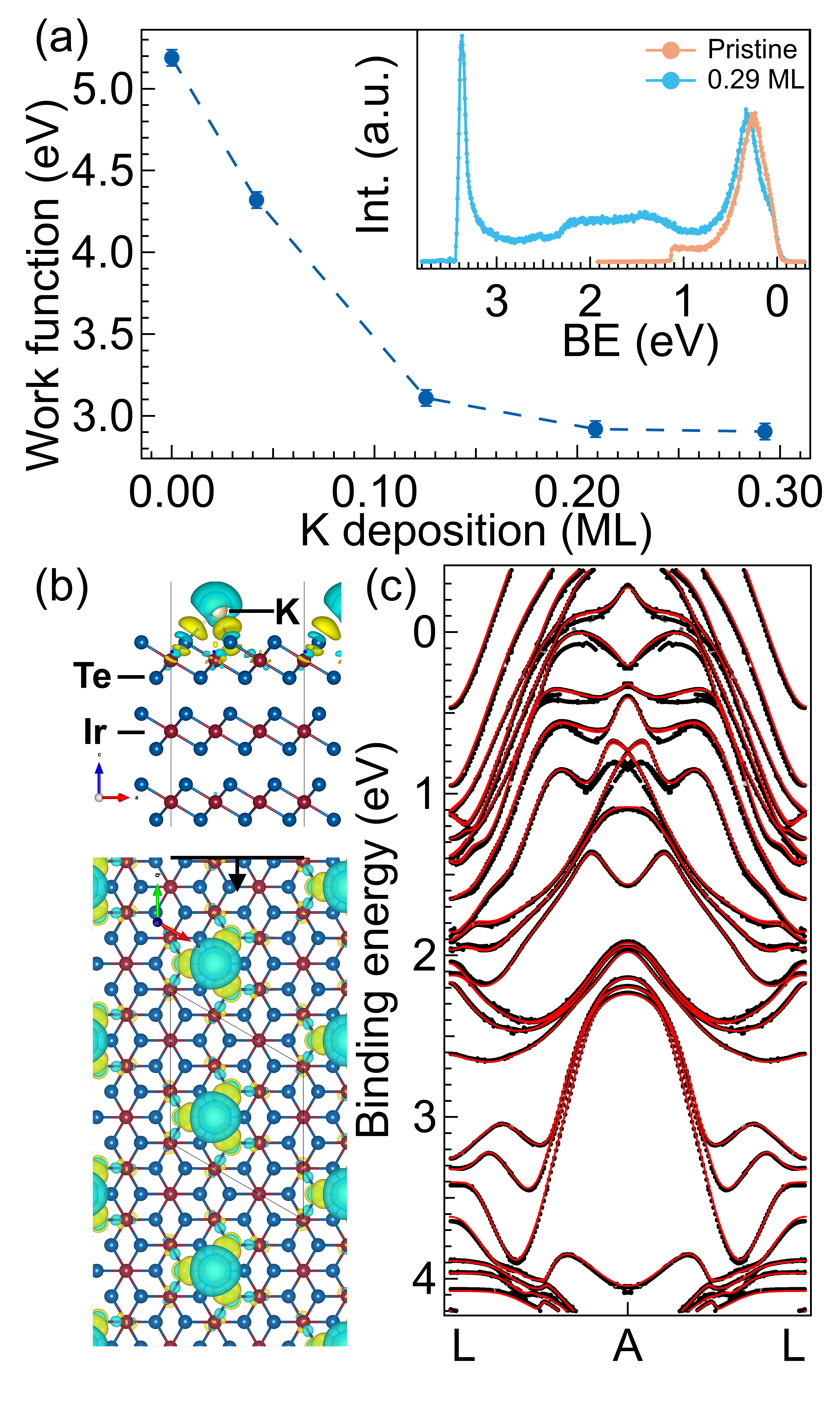
The effect of the strong electron doping induced by adsorption of ML of K at the surface is also visible on the calculated electronic band structure in Fig. 1 (c) along the A-L direction of the three-dimensional (3D) Brillouin zone (BZ) [see Fig. 2 (a)]. The red and black band structures correspond to the pristine and K-doped IrTe2 structures, respectively. The main changes occur within the first eV below the Fermi level with a shift of the surface-related electronic states towards higher BE. In particular, the band located at the A point around eV below is shifted by almost meV down to high BE and is flattened. This band is known to be a surface state Rumo et al. 2020; Bahramy et al. 2017 (SS) and is consequently strongly affected by the surface doping, as discussed below.
III.2 Electronic structure at room temperature

We have performed ARPES measurements as a function of K-deposition at RT to further discriminate the changes in the electronic structure of IrTe2. Figure 2 (a) presents the 3D BZ and its surface projection. A RT Fermi surface (integrated over eV around ) is shown in Figure 2 (b), obtained with a photon energy eV. At this photon energy, states close to the ALH plane are probed Ootsuki et al. 2013; Ootsuki et al. 2014; Ootsuki et al. 2019. In Fig. 2 (c), ARPES spectra taken at RT along the AL direction for a pristine crystal, as well as for , , and ML K-doped crystals are displayed. Corresponding energy distribution curves (EDC) integrated on a small momentum range ( Å-1) around A are shown in Figure 2 (d). On the pristine crystal [Fig. 2 (c), left panels], the electronic bands are sharp and, by comparison with the literature Lee et al. 2017; Bahramy et al. 2017; Rumo et al. 2020, we can identify the presence of bulk state B1 just below , a second bulk band B2, and an intense surface state SS at about eV BE Rumo et al. 2020. With the increase of K doping, the surface state SS flattens and shifts towards higher BE from (pristine crystal) to eV ( ML K-doped crystal) (also see the corresponding EDCs integrated around A in Fig. 2 (d)). Note that a second surface state SS2 near exhibits a similar shift to higher BE [see Fig. 2 (c)]. These observations are in line with the prediction obtained from our DFT calculations of Fig. 1 (c), especially with respect to the surface states SS and SS2. Figure 2 (e) reports the relative shift of the surface state SS () at A as a function of K doping [see also the blue markers in Figure 2 (c)], which follows the same trend as the work function [see Fig. 1 (a)].
Overall, the K adsorption at the surface of metallic IrTe2 produces a shift of the surface states, as already observed in numerous materials Hossain et al. 2008; Boyle et al. 2019; Kremer et al. 2020. However, IrTe2 is a singular material since it undergoes a series of charge-ordered phase transitions upon cooling Rumo et al. 2020; Mauerer et al. 2016; Ko et al. 2015; Li et al. 2014b; Lee et al. 2017. Consequently, a crucial point to address is the impact of K surface doping on such structural instabilities.
III.3 Temperature dependence in ARPES
We have thus performed temperature-dependent ARPES measurements with a particular focus on the energy position of the surface state at around 1 eV BE that can be used as a marker of the phase transitions Rumo et al. 2020, since its BE depends strongly on the Ir-Ir dimer length in the stripe phases. In Fig. 3 (a), we recall schematically the structure of the basic building blocks for the Ir atoms in the different phases in IrTe2. The () phase is composed only of equivalent atoms, leading to the surface state SS at about eV BE. In the () phase, five atoms split into two dimerized Ir atoms (one dimer) and three undimerized atoms [Fig. 3 (a)]. This leads to a splitting of the surface state SS into a contribution due to the dimerized Ir atoms, named SSD, at higher binding energy, and a contribution due to the three undimerized Ir atoms, named SS3. In the () and in the phases [Fig. 3 (a)], the sequence of Ir atoms changes further, implying a different combination of dimerized and undimerized atoms. At the same time, the Ir-Ir dimer length has been shown to reduce further across these phase transitions Pascut et al. 2014a; Hsu et al. 2013.

Figure 3 (b) displays ARPES spectra taken at K , K and K , along AL direction for a K coverage of ML (see all ARPES data in the Appendix VII.2). At K, sharp electronic states are clearly observed on the left panel. The surface state SS is easily distinguishable at a BE of eV. For temperatures below , the electronic states become more intricate due to the appearance of new translational symmetry of the charge-ordered phases of mixed orientations Hsu et al. 2013. A multitude of folded bands can be identified, especially in the BE range between and eV, see Fig. 3 (b). At K, in the () phase, the surface state SS is split into two states, namely SS3 and SSD, the BE of the latter being now 1.4 eV. At K, in the ()-dominated phase [see right panels in Fig. 3 (b)], SSD shifts further to higher BE reaching eV. Figure 3 (c) shows EDCs at the energy of the surface state integrated on a small momentum range ( Å-1) around A together with the corresponding fits, consisting of a single Gauss function, for temperatures down to K. The resulting shift of the surface state SSD in BE, , is defined as the difference between the surface state SS RT value for a given doping and the surface state SSD value at a temperature for the same doping [see also the colored markers in Fig. 3 (b)]. It is displayed for the pristine crystal (same data as in Ref. Rumo et al. 2020) as well as for the present ML K-doped crystal and for an additional doping of ML as a function of temperature in Fig. 3 (d). It allows us to compare directly the evolution of SSD with and without potassium.
Interestingly, the magnitudes of upon cooling through all three first-order phase transitions (, and K) for the ML K-doped crystal are not only nearly indistinguishable from pristine IrTe2, but also from a more K-doped sample ( ML). This indicates that the phase transitions are remarkably insensitive to K deposition at these values of K doping.
III.4 Temperature dependence in LEED
To support the conclusions drawn from ARPES, we have also checked the periodicities of the stripe phases of the ML K-doped crystal of IrTe2 with LEED. Figure 4 (a) displays the line profiles of LEED images taken at different temperatures (upon cooling) specific to the different phases of IrTe2, see Fig. 4 (b). They confirm the presence of the () phase at K, the () phase at K, the () phase at K and the () phase at K. Note that due to the unavoidable mixture of domains of different orientations Chen et al. 2017; Machida et al. 2013, lines of superstructure spots are observed in the three-fold symmetry equivalent directions (see in particular the LEED image at 30 K for the () phase). Furthermore, below , we observe coexistence of domains of the () phase and of the () phase (see Appendix VII.2), a pattern already observed for pristine crystals Chen et al. 2017; Rumo et al. 2020. Our complementary LEED study therefore confirms that the deposition of K atoms does not change the periodicities of the stripe phases observed across the phase transitions at the surface of IrTe2.

IV Discussion
In this work, we report that K doping shifts the surface states SS at RT to higher BE, without inducing surface reconstruction (see LEED image at RT Fig. 4). This energy shift is due to a decrease of the surface potential, as observed for instance on the Au(111) surface Forster et al. 2006, and is therefore not related to any dimerization. This is further confirmed by the absence of the split surface state SSD at RT (see Fig. 2). However, the energy shift of the surface state of the dimerized atoms, SSD, at low temperature across the phase transitions (see Fig. 3) does not vary with the K coverage used in this work. As motivated in our previous work Rumo et al. 2020, this means that the dimer length does not change and that the charge-ordered phase transitions are not modified by the surface K doping.
In contrast, many layered materials turn out to be very sensitive to alkali doping. For instance, the CDW phase in the TMDC TiSe2 is already completely suppressed at about 0.1 ML of Rb coverage Rossnagel 2010. The band gap of the semiconducting layered-material black phosphorous is very sensitive to alkali doping, already decreasing above ML and this material has been shown to undergo a semiconductor-semimetal transition at ML Kim et al. 2015a. The same effect has been discovered also in Ta2NiSe5 Fukutani et al. 2019, for which a semiconductor-semimetal transition occurs at about ML of K doping Chen et al. 2020. These recent results on low-dimensional layered materials emphasize the surprising insensitivity of IrTe2 to K doping at low coverages.
What is then the reason for this robustness of the surface transitions in IrTe2? IrTe2 has a metallic behavior above and below the phase transitions, with a significant density of states maintained at the Fermi level Fang et al. 2013; Pascut et al. 2014b, in contrast with the materials mentioned above. This is due to the fact that a dramatic reduction of density of states is observed only for the bonding and antibonding dimer states that are not lying close to Saleh and Artyukhin 2020; Pascut et al. 2014b; Ideta et al. 2018; Kim et al. 2015b. Away from these dimer states the density of states is insignificantly affected by the phase transitions Pascut et al. 2014b. This naturally makes the charge-ordered phase transitions in IrTe2 insensitive to carrier doping, for three reasons. (1) Screening of the electric field of the ionized doping atoms is more efficient for a metallic surface. This excludes the possibility of a large unscreened electric field near the surface, which is central to the phase transition in black phosphorus for instance Kim et al. 2015a. (2) When electron doping changes the low-energy band structure, and thus the corresponding Fermi surface shape, it can significantly alter the electronic susceptibility of materials, reducing their tendency to instabilities, as for instance in TiSe2 Jaouen et al. 2019 or Ta2NiSe5 Fukutani et al. 2019. This mechanism is often the cause of the suppression of a collective instability, like a charge density wave, by alkali doping. However, the low-energy electronic structure of IrTe2 is little modified by a given electron doping density in a rigid band model picture, since the high density of states at can easily accommodate the doping electrons. (3) Finally, the doping charge does not populate the antibonding states that are further away from , since the nonbonding states near likely capture the K doping electron. This prevents the destabilization of Ir dimers. Furthermore, we recall here that our DFT calculations indicate that the charge transfer from the K adatom affects only the top surface layer and mainly dopes the surface states, a fact confirmed by our ARPES data, so that the bulk electronic structure stays unchanged. We further emphasize that, despite this surface doping, it is surprising that the phase transition, which occurs only at the surface, is not affected. It demonstrates that purely electronic doping is not the most efficient way to destabilize the charge-ordered phases of IrTe2. Therefore, our results support the idea that the instability is driven by a local mechanism mainly involving the atoms forming the dimers, stabilized by a large electronic energy gain due to the creation of the bonding-antibonding states of these dimers Pascut et al. 2014b; Pascut et al. 2014a; Saleh and Artyukhin 2020.
In contrast, recent literature reveals that structural perturbation, as induced by chemical substitution Pyon et al. 2012; Oh et al. 2013; Yang et al. 2017 or applied strain Nicholson et al. 2021, is much more efficient at altering the phase diagram. More specifically for of Pt or Pd substitution, which kills the charge order in favor of superconductivity, a gain of per unit cell throughout the crystal is achieved, while in our case per unit cell localized at the surface is observed from our calculations. However, the chemical substitution causes a local strain in the lattice. For example, Pd has an atomic size difference of with Te, which creates distortions in the lattice, which itself contributes to the phase transitions. This is much greater than the mechanical strain which is observed to stabilise the phase. The phase transitions are strongly disturbed in these particular cases while pure electronic doping is unable to induce such an effect. This is consistent with the results of a recent time-resolved ARPES study Monney et al. 2018 that concluded that infrared photoexcitation cannot efficiently trigger the phase transition and that only a partial photoinduced phase transition occurs, driven by the transient heating of the lattice.
V Conclusion
In this work, we have studied the influence of K-doping on IrTe2 with ARPES and LEED, supported by DFT calculations. We have performed a detailed and systematic analysis as a function of K deposition at RT and we have probed the occurrence of charge-ordered phases as a function of temperature. We have shown that the perturbation by electronic doping from the alkali atoms has no effect on the charge-ordered phase transitions at the surface of IrTe2. This emphasizes the important role of the structural component in the stabilization of these phases. In this framework, it will be particularly interesting to test the stability of the charge-ordered phases of IrTe2 in the limit of a single monolayer or within of van der Waals heterostructures.
VI Acknowledgments
This project was supported from the Swiss National Science Foundation (SNSF) Grant No. P00P2_170597. A.P. acknowledges the Osk. Huttunen Foundation for financial support, and CSC – IT Center for Science, Finland, for computational resources. We are very grateful to P. Aebi for fruitful discussions and for sharing with us his photoemission setup. Skillful technical assistance was provided by F. Bourqui, B. Hediger, J.L. Andrey, O. Raetzo and M. Andrey.
VII Appendices
VII.1 K deposition calibration

Figure 5 shows a high-resolution STM image taken on a K-doped IrTe2 crystal of the occupied states at a bias voltage of mV and a constant current mode of nA with atomic resolution. The K deposition was performed at RT. The STM image [Fig. 5] reveals the presence of adsorbed K atoms at the surface as bright protrusions on top of the low temperature reconstruction of IrTe2. From the statistics made on a few images, a K coverage of ML is estimated for an exposition time to the SAES getter source of s (one K atom per IrTe2 surface unit cell at RT is defined as ML of K atom).
We caution that this STM measurement reveals only adsorbed K atoms at the surface of IrTe2. However, intercalation of K atoms in the van der Waals gap could also occur in parallel to adsorption, as reported in the literature for TaS2 or graphite Rossnagel 2010; Caragiu and Finberg 2005; Ramírez et al. 2006. We stress that the distance between two sandwiches of IrTe2 (interlayer spacing) is smaller (about Å) than for most TMDCs and for graphite ( Å). Therefore we expect alkali intercalation to be unfavorable for the present case.
VII.2 Supplementary data for the temperature dependent study
Figure 6 displays a LEED image of the ML K doped IrTe2 showing both the () and the () phases at K, as observed in the pristine IrTe2 case for the same temperature.

Figure 7 displays the evolution of the temperature of the sample during the temperature dependent ARPES measurements. The cooling rate is less than 3 K/min and on average less than K/min.

Figure 8 (a) shows ARPES spectra taken at different temperatures during the cooling process, , , , , , , , , , , , , and K on a ML K-doped crystal of IrTe2. The evolution of the electronic structure of a ML K-doped crystal of IrTe2 can be observed and in particular the shift of the surface state as a function of temperature. Figure 8 (b) displays Fermi surfaces of a ML K-doped IrTe2 crystal at different temperatures.

References
- Rossnagel (2011) K. Rossnagel, Journal of Physics: Condensed Matter 23, 213001 (2011), URL https://doi.org/10.1088/0953-8984/23/21/213001.
- Johannes and Mazin (2008) M. D. Johannes and I. I. Mazin, Phys. Rev. B 77, 165135 (2008), URL https://link.aps.org/doi/10.1103/PhysRevB.77.165135.
- Pyon et al. (2012) S. Pyon, K. Kudo, and M. Nohara, Journal of the Physical Society of Japan 81, 053701 (2012), URL https://doi.org/10.1143/JPSJ.81.053701.
- Morosan et al. (2006) E. Morosan, H. W. Zandbergen, B. S. Dennis, J. W. G. Bos, Y. Onose, T. Klimczuk, A. P. Ramirez, N. P. Ong, and R. J. Cava, Nature Physics 2, 544 (2006), ISSN 1745-2481, URL https://doi.org/10.1038/nphys360.
- Sipos et al. (2008) B. Sipos, A. F. Kusmartseva, A. Akrap, H. Berger, L. Forró, and E. Tutiš, Nature Materials 7, 960 (2008), ISSN 1476-4660, URL https://doi.org/10.1038/nmat2318.
- Yang et al. (2017) H. Yang, S. W. Kim, M. Chhowalla, and Y. H. Lee, Nature Physics 13, 931 (2017), URL https://doi.org/10.1038/nphys4188.
- Chernikov et al. (2014) A. Chernikov, T. C. Berkelbach, H. M. Hill, A. Rigosi, Y. Li, O. B. Aslan, D. R. Reichman, M. S. Hybertsen, and T. F. Heinz, Phys. Rev. Lett. 113, 076802 (2014), URL https://link.aps.org/doi/10.1103/PhysRevLett.113.076802.
- Mak et al. (2012) K. F. Mak, K. He, J. Shan, and T. F. Heinz, Nature Nanotechnology 7, 494 (2012), ISSN 1748-3395.
- Zeng et al. (2012) H. Zeng, J. Dai, W. Yao, D. Xiao, and X. Cui, Nature Nanotechnology 7, 490 (2012), ISSN 1748-3395, URL https://doi.org/10.1038/nnano.2012.96.
- Riley et al. (2014) J. M. Riley, F. Mazzola, M. Dendzik, M. Michiardi, T. Takayama, L. Bawden, C. Granerød, M. Leandersson, T. Balasubramanian, M. Hoesch, et al., Nature Physics 10, 835 (2014), ISSN 1745-2481, URL https://doi.org/10.1038/nphys3105.
- Bertoni et al. (2016) R. Bertoni, C. W. Nicholson, L. Waldecker, H. Hübener, C. Monney, U. De Giovannini, M. Puppin, M. Hoesch, E. Springate, R. T. Chapman, et al., Phys. Rev. Lett. 117, 277201 (2016), URL https://link.aps.org/doi/10.1103/PhysRevLett.117.277201.
- Tamai et al. (2016) A. Tamai, Q. S. Wu, I. Cucchi, F. Y. Bruno, S. Riccò, T. K. Kim, M. Hoesch, C. Barreteau, E. Giannini, C. Besnard, et al., Phys. Rev. X 6, 031021 (2016), URL https://link.aps.org/doi/10.1103/PhysRevX.6.031021.
- Wu et al. (2016) Y. Wu, D. Mou, N. H. Jo, K. Sun, L. Huang, S. L. Bud’ko, P. C. Canfield, and A. Kaminski, Phys. Rev. B 94, 121113(R) (2016), URL https://link.aps.org/doi/10.1103/PhysRevB.94.121113.
- Bahramy et al. (2017) M. S. Bahramy, O. J. Clark, B.-J. Yang, J. Feng, L. Bawden, J. M. Riley, I. Markovic, F. Mazzola, V. Sunko, D. Biswas, et al., Nature Materials 17, 21 (2017), URL https://doi.org/10.1038/nmat5031.
- Stojchevska et al. (2014) L. Stojchevska, I. Vaskivskyi, T. Mertelj, P. Kusar, D. Svetin, S. Brazovskii, and D. Mihailovic, Science 344, 177 (2014), ISSN 0036-8075, URL https://science.sciencemag.org/content/344/6180/177.
- Oike et al. (2018) H. Oike, M. Kamitani, Y. Tokura, and F. Kagawa, Science Advances 4 (2018), URL https://advances.sciencemag.org/content/4/10/eaau3489.
- Sie et al. (2019) E. J. Sie, C. M. Nyby, C. D. Pemmaraju, S. J. Park, X. Shen, J. Yang, M. C. Hoffmann, B. K. Ofori-Okai, R. Li, A. H. Reid, et al., Nature 565, 61 (2019), ISSN 1476-4687, URL https://doi.org/10.1038/s41586-018-0809-4.
- Nicholson et al. (2021) C. W. Nicholson, M. Rumo, A. Pulkkinen, G. Kremer, B. Salzmann, M.-L. Mottas, B. Hildebrand, T. Jaouen, T. K. Kim, S. Mukherjee, et al., Communications Materials 2, 25 (2021), ISSN 2662-4443, URL https://doi.org/10.1038/s43246-021-00130-5.
- Rossnagel (2010) K. Rossnagel, New Journal of Physics 12, 125018 (2010), URL https://doi.org/10.1038/nphys4188.
- Jaouen et al. (2019) T. Jaouen, M. Rumo, B. Hildebrand, M. L. Mottas, C. W. Nicholson, G. Kremer, B. Salzmann, F. Vanini, C. Barreteau, E. Giannini, et al. (2019), eprint 1911.06053.
- Kim et al. (2015a) J. Kim, S. S. Baik, S. H. Ryu, Y. Sohn, S. Park, B.-G. Park, J. Denlinger, Y. Yi, H. J. Choi, and K. S. Kim, Science 349, 723 (2015a), ISSN 0036-8075, URL https://science.sciencemag.org/content/349/6249/723.
- Fukutani et al. (2019) K. Fukutani, R. Stania, J. Jung, E. F. Schwier, K. Shimada, C. I. Kwon, J. S. Kim, and H. W. Yeom, Phys. Rev. Lett. 123, 206401 (2019), URL https://link.aps.org/doi/10.1103/PhysRevLett.123.206401.
- Pascut et al. (2014a) G. L. Pascut, T. Birol, M. J. Gutmann, J. J. Yang, S.-W. Cheong, K. Haule, and V. Kiryukhin, Phys. Rev. B 90, 195122 (2014a), URL https://link.aps.org/doi/10.1103/PhysRevB.90.195122.
- Mauerer et al. (2016) T. Mauerer, M. Vogt, P.-J. Hsu, G. L. Pascut, K. Haule, V. Kiryukhin, J. Yang, S.-W. Cheong, W. Wu, and M. Bode, Phys. Rev. B 94, 014106 (2016), URL https://link.aps.org/doi/10.1103/PhysRevB.94.014106.
- Hsu et al. (2013) P.-J. Hsu, T. Mauerer, M. Vogt, J. J. Yang, Y. S. Oh, S.-W. Cheong, M. Bode, and W. Wu, Phys. Rev. Lett. 111, 266401 (2013), URL https://link.aps.org/doi/10.1103/PhysRevLett.111.266401.
- Rumo et al. (2020) M. Rumo, C. W. Nicholson, A. Pulkkinen, B. Hildebrand, G. Kremer, B. Salzmann, M.-L. Mottas, K. Y. Ma, E. L. Wong, M. K. L. Man, et al., Phys. Rev. B 101, 235120 (2020), URL https://link.aps.org/doi/10.1103/PhysRevB.101.235120.
- Momma and Izumi (2011) K. Momma and F. Izumi, Journal of Applied Crystallography 44, 1272 (2011), URL https://doi.org/10.1107/S0021889811038970.
- Ko et al. (2015) K.-T. Ko, H.-H. Lee, D.-H. Kim, J.-J. Yang, S.-W. Cheong, M. J. Eom, J. S. Kim, R. Gammag, K.-S. Kim, H.-S. Kim, et al., Nature Communications 6, 7342 (2015), ISSN 2041-1723, URL https://doi.org/10.1038/ncomms8342.
- Fang et al. (2013) A. F. Fang, G. Xu, T. Dong, P. Zheng, and N. L. Wang, Scientific Reports 3, 1153 (2013), URL https://doi.org/10.1038/srep01153.
- Jobic et al. (1991) S. Jobic, P. Deniard, R. Brec, J. Rouxel, A. Jouanneaux, and A. N. Fitch, Zeitschrift für anorganische und allgemeine Chemie 598, 199 (1991), URL https://onlinelibrary.wiley.com/doi/abs/10.1002/zaac.19915980119.
- Matsumoto et al. (1999) N. Matsumoto, K. Taniguchi, R. Endoh, H. Takano, and S. Nagata, Journal of Low Temperature Physics 117, 1129 (1999), ISSN 1573-7357, URL https://doi.org/10.1023/A:1022546928480.
- Toriyama et al. (2014) T. Toriyama, M. Kobori, T. Konishi, Y. Ohta, K. Sugimoto, J. Kim, A. Fujiwara, S. Pyon, K. Kudo, and M. Nohara, Journal of the Physical Society of Japan 83, 033701 (2014), URL https://doi.org/10.7566/JPSJ.83.033701.
- Koley (2016) S. Koley, Solid State Communications 247, 40 (2016), ISSN 0038-1098, URL http://www.sciencedirect.com/science/article/pii/S0038109816302095.
- Li et al. (2014a) B. Li, G. Huang, J. Sun, and Z. Xing, Scientific Reports 4, 6433 (2014a), URL https://doi.org/10.1038/srep06433.
- Paris et al. (2016) E. Paris, B. Joseph, A. Iadecola, C. Marini, H. Ishii, K. Kudo, S. Pascarelli, M. Nohara, T. Mizokawa, and N. L. Saini, Phys. Rev. B 93, 134109 (2016), URL https://link.aps.org/doi/10.1103/PhysRevB.93.134109.
- Pascut et al. (2014b) G. L. Pascut, K. Haule, M. J. Gutmann, S. A. Barnett, A. Bombardi, S. Artyukhin, T. Birol, D. Vanderbilt, J. J. Yang, S.-W. Cheong, et al., Phys. Rev. Lett. 112, 086402 (2014b), URL https://link.aps.org/doi/10.1103/PhysRevLett.112.086402.
- Li et al. (2014b) Q. Li, W. Lin, J. Yan, X. Chen, A. G. Gianfrancesco, D. J. Singh, D. Mandrus, S. V. Kalinin, and M. Pan, Nature Communications 5, 5358 (2014b), ISSN 2041-1723, URL https://doi.org/10.1038/ncomms6358.
- Oh et al. (2013) Y. S. Oh, J. J. Yang, Y. Horibe, and S.-W. Cheong, Phys. Rev. Lett. 110, 127209 (2013), URL https://link.aps.org/doi/10.1103/PhysRevLett.110.127209.
- Takubo et al. (2014) K. Takubo, R. Comin, D. Ootsuki, T. Mizokawa, H. Wadati, Y. Takahashi, G. Shibata, A. Fujimori, R. Sutarto, F. He, et al., Phys. Rev. B 90, 081104(R) (2014), URL https://link.aps.org/doi/10.1103/PhysRevB.90.081104.
- Saleh and Artyukhin (2020) G. Saleh and S. Artyukhin, The Journal of Physical Chemistry Letters 11, 2127 (2020), pMID: 32079398.
- Dai et al. (2014) J. Dai, K. Haule, J. J. Yang, Y. S. Oh, S.-W. Cheong, and W. Wu, Phys. Rev. B 90, 235121 (2014), URL https://link.aps.org/doi/10.1103/PhysRevB.90.235121.
- Lee et al. (2017) H. Lee, K.-T. Ko, K. Kim, B.-G. Park, J. Yang, S.-W. Cheong, and J.-H. Park, Europhysics Letters 120, 47003 (2017), URL https://doi.org/10.1209/0295-5075/120/47003.
- Ootsuki et al. (2013) D. Ootsuki, S. Pyon, K. Kudo, M. Nohara, M. Horio, T. Yoshida, A. Fujimori, M. Arita, H. Anzai, H. Namatame, et al., Journal of the Physical Society of Japan 82, 093704 (2013), URL https://doi.org/10.7566/JPSJ.82.093704.
- Ootsuki et al. (2019) D. Ootsuki, H. Ishii, K. Kudo, M. Nohara, M. Arita, H. Namatame, M. Taniguchi, N. L. Saini, and T. Mizokawa, Journal of Physics and Chemistry of Solids 128, 270 (2019), ISSN 0022-3697, URL http://www.sciencedirect.com/science/article/pii/S0022369717316347.
- Yang et al. (2012) J. J. Yang, Y. J. Choi, Y. S. Oh, A. Hogan, Y. Horibe, K. Kim, B. I. Min, and S.-W. Cheong, Phys. Rev. Lett. 108, 116402 (2012), URL https://link.aps.org/doi/10.1103/PhysRevLett.108.116402.
- Kresse and Hafner (1993) G. Kresse and J. Hafner, Phys. Rev. B 47, 558 (1993), URL https://link.aps.org/doi/10.1103/PhysRevB.47.558.
- Kresse and Hafner (1994) G. Kresse and J. Hafner, Phys. Rev. B 49, 14251 (1994), URL https://link.aps.org/doi/10.1103/PhysRevB.49.14251.
- Kresse and Furthmueller (1996a) G. Kresse and J. Furthmueller, Computational Materials Science 6, 15 (1996a), ISSN 0927-0256, URL http://www.sciencedirect.com/science/article/pii/0927025696000080.
- Kresse and Furthmueller (1996b) G. Kresse and J. Furthmueller, Phys. Rev. B 54, 11169 (1996b), URL https://link.aps.org/doi/10.1103/PhysRevB.54.11169.
- Kresse and Joubert (1999) G. Kresse and D. Joubert, Phys. Rev. B 59, 1758 (1999), URL https://link.aps.org/doi/10.1103/PhysRevB.59.1758.
- Perdew et al. (1996) J. P. Perdew, K. Burke, and M. Ernzerhof, Phys. Rev. Lett. 77, 3865 (1996), URL https://link.aps.org/doi/10.1103/PhysRevLett.77.3865.
- Herath et al. (2020) U. Herath, P. Tavadze, X. He, E. Bousquet, S. Singh, F. Muñoz, and A. H. Romero, Computer Physics Communications 251, 107080 (2020), ISSN 0010-4655, URL https://www.sciencedirect.com/science/article/pii/S0010465519303935.
- Tang et al. (2009) W. Tang, E. Sanville, and G. Henkelman, Journal of Physics: Condensed Matter 21, 084204 (2009), URL https://doi.org/10.1088/0953-8984/21/8/084204.
- Sanville et al. (2007) E. Sanville, S. D. Kenny, R. Smith, and G. Henkelman, Journal of Computational Chemistry 28, 899 (2007), URL https://onlinelibrary.wiley.com/doi/abs/10.1002/jcc.20575.
- Henkelman et al. (2006) G. Henkelman, A. Arnaldsson, and H. Jónsson, Computational Materials Science 36, 354 (2006), ISSN 0927-0256, URL http://www.sciencedirect.com/science/article/pii/S0927025605001849.
- Yu and Trinkle (2011) M. Yu and D. R. Trinkle, The Journal of Chemical Physics 134, 064111 (2011), URL https://doi.org/10.1063/1.3553716.
- Ootsuki et al. (2014) D. Ootsuki, T. Toriyama, M. Kobayashi, S. Pyon, K. Kudo, M. Nohara, T. Sugimoto, T. Yoshida, M. Horio, A. Fujimori, et al., Journal of the Physical Society of Japan 83, 033704 (2014), URL https://doi.org/10.7566/JPSJ.83.033704.
- Hossain et al. (2008) M. A. Hossain, J. D. F. Mottershead, D. Fournier, A. Bostwick, J. L. McChesney, E. Rotenberg, R. Liang, W. N. Hardy, G. A. Sawatzky, I. S. Elfimov, et al., Nature Physics 4, 527 (2008), ISSN 1745-2481, URL https://doi.org/10.1038/nphys998.
- Boyle et al. (2019) T. J. Boyle, A. Rossi, M. Walker, P. Carlson, M. K. Miller, J. Zhao, P. Klavins, C. Jozwiak, A. Bostwick, E. Rotenberg, et al., Phys. Rev. B 100, 081105(R) (2019), URL https://link.aps.org/doi/10.1103/PhysRevB.100.081105.
- Kremer et al. (2020) G. Kremer, T. Jaouen, B. Salzmann, L. Nicolaï, M. Rumo, C. W. Nicholson, B. Hildebrand, J. H. Dil, J. Minár, G. Springholz, et al., Phys. Rev. Research 2, 033115 (2020), URL https://link.aps.org/doi/10.1103/PhysRevResearch.2.033115.
- Chen et al. (2017) C. Chen, J. Kim, Y. Yang, G. Cao, R. Jin, and E. W. Plummer, Phys. Rev. B 95, 094118 (2017), URL https://link.aps.org/doi/10.1103/PhysRevB.95.094118.
- Machida et al. (2013) T. Machida, Y. Fujisawa, K. Igarashi, A. Kaneko, S. Ooi, T. Mochiku, M. Tachiki, K. Komori, K. Hirata, and H. Sakata, Phys. Rev. B 88, 245125 (2013), URL https://link.aps.org/doi/10.1103/PhysRevB.88.245125.
- Forster et al. (2006) F. Forster, A. Bendounan, J. Ziroff, and F. Reinert, Surface Science 600, 3870 (2006), ISSN 0039-6028, berlin, Germany: 4–9 September 2005, URL https://www.sciencedirect.com/science/article/pii/S0039602806004158.
- Chen et al. (2020) L. Chen, T. T. Han, C. Cai, Z. G. Wang, Y. D. Wang, Z. M. Xin, and Y. Zhang, Phys. Rev. B 102, 161116(R) (2020), URL https://link.aps.org/doi/10.1103/PhysRevB.102.161116.
- Ideta et al. (2018) S.-i. Ideta, D. Zhang, A. G. Dijkstra, S. Artyukhin, S. Keskin, R. Cingolani, T. Shimojima, K. Ishizaka, H. Ishii, K. Kudo, et al., Science Advances 4 (2018), URL https://advances.sciencemag.org/content/4/7/eaar3867.
- Kim et al. (2015b) K. Kim, S. Kim, K.-T. Ko, H. Lee, J.-H. Park, J. J. Yang, S.-W. Cheong, and B. I. Min, Phys. Rev. Lett. 114, 136401 (2015b), URL https://link.aps.org/doi/10.1103/PhysRevLett.114.136401.
- Monney et al. (2018) C. Monney, A. Schuler, T. Jaouen, M.-L. Mottas, T. Wolf, M. Merz, M. Muntwiler, L. Castiglioni, P. Aebi, F. Weber, et al., Phys. Rev. B 97, 075110 (2018), URL https://link.aps.org/doi/10.1103/PhysRevB.97.075110.
- Caragiu and Finberg (2005) M. Caragiu and S. Finberg, Journal of Physics: Condensed Matter 17, R995 (2005), URL https://doi.org/10.1088/0953-8984/17/35/r02.
- Ramírez et al. (2006) C. Ramírez, R. Adelung, L. Kipp, and W. Schattke, Phys. Rev. B 73, 195406 (2006), URL https://link.aps.org/doi/10.1103/PhysRevB.73.195406.